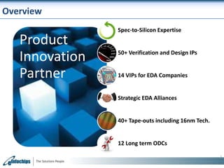
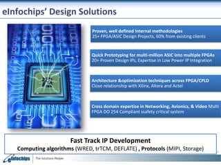
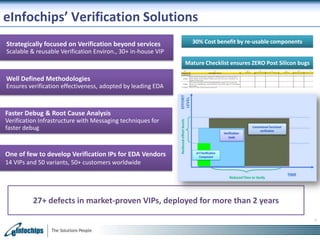
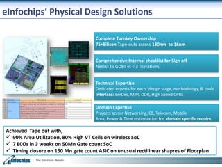
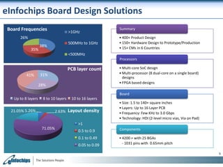
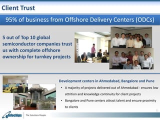
eInfochips Semiconductor Solutions
Agenda
Overview
Semiconductor Division

Semiconductor Offerings
Tools Expertise
Client Relationships

Success Stories
2
Overview

Product
Innovation
Partner

Spec-to-Silicon Expertise

50+ Verification and Design IPs

14 VIPs for EDA Companies

Strategic EDA Alliances

40+ Tape-outs including 16nm Tech.

12 Long term ODCs
3
Semiconductor Division

16+

12

150+

30+

20+

Years of Experience

Tier-1 ODCs

First Pass Success

Verification IPs

Design IPs

Globally #1 in Silicon Design
Services

4
Offerings

Silicon Design

Reference Design

Product Design

Partner with R&D to
tape-out flawless
Silicon on schedule

Empower Sales to
showcase features of
new silicon platforms

Enable your Clients to
build custom products
using latest Silicon

SoC / ASIC Design
SoC Verification
Physical Design
Silicon Validation
5
eInfochips’ Design Solutions
Proven, well defined Internal methodologies
25+ FPGA/ASIC Design Projects, 60% from existing clients

Quick Prototyping for multi-million ASIC into multiple FPGAs
20+ Proven Design IPs, Expertise in Low Power IP Integration

Architecture &optimization techniques across FPGA/CPLD
Close relationship with Xilinx, Altera and Actel

Cross domain expertise in Networking, Avionics, & Video Multi
FPGA DO 254 Compliant ssafety critical system

Fast Track IP Development
Computing algorithms (WRED, trTCM, DEFLATE) , Protocols (MIPI, Storage)

6
eInfochips’ Verification Solutions
Strategically focused on Verification beyond services

30% Cost benefit by re-usable components

Scalable & reusable Verification Environ., 30+ in-house VIP
Mature Checklist ensures ZERO Post Silicon bugs

Well Defined Methodologies
Ensures verification effectiveness, adopted by leading EDA

Faster Debug & Root Cause Analysis
Verification Infrastructure with Messaging techniques for
faster debug

One of few to develop Verification IPs for EDA Vendors
14 VIPs and 50 variants, 50+ customers worldwide

27+ defects in market-proven VIPs, deployed for more than 2 years
7
eInfochips’ Physical Design Solutions
Complete Turnkey Ownership
75+Silicon Tape-outs across 180nm to 16nm
Comprehensive Internal checklist for Sign off
Netlist to GDSII in < 3 iterations
Technical Expertise
Dedicated experts for each design stage, methodology, & tools
Interface: SerDes, MIPI, DDR, High Speed CPUs

Domain Expertise
Projects across Networking, CE, Telecom, Mobile
Area, Power & Time optimization for domain specific require.

Achieved Tape out with,
 90% Area Utilization, 80% High VT Cells on wireless SoC
 7 ECOs in 3 weeks on 50Mn Gate count SoC
 Timing closure on 150 Mn gate count ASIC on unusual rectilinear shapres of Floorplan
eInfochips Board Design Solutions
Board Frequencies

>1GHz

26%
35%

500MHz to 1GHz

38%

Summary
• 400+ Product Design
• 150+ Hardware Design to Prototype/Production
• 15+ CMs in 6 Countries

<500MHz
Processors

PCB layer count
41%

31%
28%

• Multi-core SoC design
• Multi-processor (8 dual-core on a single board)
designs
• FPGA based designs
Board

Up to 8 layers

8 to 10 layers

10 to 16 layers

2.63% Layout density

21.05% 5.26%

• Size: 1.5 to 140+ square inches
• Layers: Up to 16 Layer PCB
• Frequency: Few KHz to 3.0 Gbps
• Technology: HDI (2-level micro vias, Via on Pad)

>1
71.05%

0.5 to 0.9

Components

0.1 to 0.49

• 4200 + with 25 BGAs
- 1031 pins with 0.65mm pitch

0.05 to 0.09

9
eInfochips Confidential
Tools & Platforms Expertise
Design Tools

Vertex
Spartan
Kintex

• Cadence OrCAD
• Mentor DxDesigner
• Allegro
• PADS
• Expedition
• Betasoft
• Hyperlinx
• Spectra-Quest

ASIC Design
•QuestaSim
•Modelsim
•VCS
•Design & DFT Compiler
•PT

Cyclone
Flex
Nios

A3P Series

FPGA Design
•Synplify-Pro
•Xilinx-ISE
•Altera-QuartusII
•Actel-Libero
•ChipScope
•SignalTapII
•Leonardo Spectrum
•PCie Analyzer
•Logic Analyzer
•O-Scope
•CHIPit-PlatinumV4
•HAPS Board
•Palladium, EVE

Verification
•IUS
•NC-Sim
•Conformal
•Questasim
•Modelsim
•Formality
•FinSim, VeriLint
•exploreRTL, LEDA
•Verix, SureCov
•CoverMeter
•HDLScore
•NextGen MVRC
•IUS LP, CLP LEC

Implementation
•Magma Talus
•Blast & Quartz
•Synopsys DC
•ICC, Astro
•PrimeTime, PTSI
•TetraMAX
•StarRC XT
•MG Calibre
•SoC Encounter
•Celtic, Nanoroute
•Virtuoso, Conformal LEC

10
eInfochips Confidential
Client Trust
95% of business from Offshore Delivery Centers (ODCs)
5 out of Top 10 global
semiconductor companies trust
us with complete offshore
ownership for turnkey projects

Development centers in Ahmedabad, Bangalore and Pune
• A majority of projects delivered out of Ahmedabad - ensures low
attrition and knowledge continuity for client projects
• Bangalore and Pune centers attract talent and ensure proximity
to clients
11
Client Relationships
8 of our Top-10 Clients have been with us for 3+ years
• Average engagement duration for top-10 client ODCs is 4.5 years
• Maximum ODC engagement duration is 12 years, and counting!
•

Turnkey Ownership - Value Creation beyond staff-augmentation

•

Top semiconductor companies have audited and recommended our ODC infrastructure
and delivery capabilities

12
ODC Snapshot
Global Data Networking Giant
• 7 Tape-outs, first pass silicon
• Clean GDSII for 150M Gate, 1GHz SoC
• Proven Offshore Checklist and Delivery, < 5% Schedule Variance
• Methodology Enabler for CTS, Floorplan
Three 28nm ASICs
Two 40nm ASICs
40nm Multiple ASIC Switch
65nm Router Switch

13
ODC Snapshot
A Leading EDA Tools Company
• Developed and maintained 13 VIPs, Supported 30 Variants

• Verification Tool Validation, validation of latest Low Power Features
Low Power, Tool Validation 5 VIPs
Memory Models 2 VIPs
UMM / VMM Enabled 8 VIPs
OpenVera VIP

14
Accolades
“Thank you all for your support and
professional work. It has been a unique
experience - I never had any close
encounters with your country and culture.”
- Japanese electronics conglomerate
“Would like to thank you for your exemplary
efforts in helping us tape out in a timely, efficient
and productive manner.”
- Leading manufacturer of networking equipment
“worked with diligence & appreciate the
perseverance in performing the difficult task
of narrowing platform behavior on RTL
simulation”
- World's largest semiconductor chip maker

“Appreciate eInfochips for their
thoroughness in DO-254 compliant
development, which delighted our end
customer”
- Leading Aerospace Solutions provider

15
Why eInfochips

 Matured Processes and Internal Checklists
Evolved over 16 years of delivery excellence in ASIC

 Early access to tools & technologies
Strategic Alliances with EDA and FPGA companies, to achieve a competitive edge
 Proven Design and Verification IPs
Ensuring high performance, reliability & manufacturability, at lower cost
16
Thank you

For more information,
write us at marketing@einfochips.com
or visit www.einfochips.com

eInfochips Semiconductor Services

  • 1.
  • 2.
    Agenda Overview Semiconductor Division Semiconductor Offerings ToolsExpertise Client Relationships Success Stories 2
  • 3.
    Overview Product Innovation Partner Spec-to-Silicon Expertise 50+ Verificationand Design IPs 14 VIPs for EDA Companies Strategic EDA Alliances 40+ Tape-outs including 16nm Tech. 12 Long term ODCs 3
  • 4.
    Semiconductor Division 16+ 12 150+ 30+ 20+ Years ofExperience Tier-1 ODCs First Pass Success Verification IPs Design IPs Globally #1 in Silicon Design Services 4
  • 5.
    Offerings Silicon Design Reference Design ProductDesign Partner with R&D to tape-out flawless Silicon on schedule Empower Sales to showcase features of new silicon platforms Enable your Clients to build custom products using latest Silicon SoC / ASIC Design SoC Verification Physical Design Silicon Validation 5
  • 6.
    eInfochips’ Design Solutions Proven,well defined Internal methodologies 25+ FPGA/ASIC Design Projects, 60% from existing clients Quick Prototyping for multi-million ASIC into multiple FPGAs 20+ Proven Design IPs, Expertise in Low Power IP Integration Architecture &optimization techniques across FPGA/CPLD Close relationship with Xilinx, Altera and Actel Cross domain expertise in Networking, Avionics, & Video Multi FPGA DO 254 Compliant ssafety critical system Fast Track IP Development Computing algorithms (WRED, trTCM, DEFLATE) , Protocols (MIPI, Storage) 6
  • 7.
    eInfochips’ Verification Solutions Strategicallyfocused on Verification beyond services 30% Cost benefit by re-usable components Scalable & reusable Verification Environ., 30+ in-house VIP Mature Checklist ensures ZERO Post Silicon bugs Well Defined Methodologies Ensures verification effectiveness, adopted by leading EDA Faster Debug & Root Cause Analysis Verification Infrastructure with Messaging techniques for faster debug One of few to develop Verification IPs for EDA Vendors 14 VIPs and 50 variants, 50+ customers worldwide 27+ defects in market-proven VIPs, deployed for more than 2 years 7
  • 8.
    eInfochips’ Physical DesignSolutions Complete Turnkey Ownership 75+Silicon Tape-outs across 180nm to 16nm Comprehensive Internal checklist for Sign off Netlist to GDSII in < 3 iterations Technical Expertise Dedicated experts for each design stage, methodology, & tools Interface: SerDes, MIPI, DDR, High Speed CPUs Domain Expertise Projects across Networking, CE, Telecom, Mobile Area, Power & Time optimization for domain specific require. Achieved Tape out with,  90% Area Utilization, 80% High VT Cells on wireless SoC  7 ECOs in 3 weeks on 50Mn Gate count SoC  Timing closure on 150 Mn gate count ASIC on unusual rectilinear shapres of Floorplan
  • 9.
    eInfochips Board DesignSolutions Board Frequencies >1GHz 26% 35% 500MHz to 1GHz 38% Summary • 400+ Product Design • 150+ Hardware Design to Prototype/Production • 15+ CMs in 6 Countries <500MHz Processors PCB layer count 41% 31% 28% • Multi-core SoC design • Multi-processor (8 dual-core on a single board) designs • FPGA based designs Board Up to 8 layers 8 to 10 layers 10 to 16 layers 2.63% Layout density 21.05% 5.26% • Size: 1.5 to 140+ square inches • Layers: Up to 16 Layer PCB • Frequency: Few KHz to 3.0 Gbps • Technology: HDI (2-level micro vias, Via on Pad) >1 71.05% 0.5 to 0.9 Components 0.1 to 0.49 • 4200 + with 25 BGAs - 1031 pins with 0.65mm pitch 0.05 to 0.09 9 eInfochips Confidential eInfochips Confidential
  • 10.
    Tools & PlatformsExpertise Design Tools Vertex Spartan Kintex • Cadence OrCAD • Mentor DxDesigner • Allegro • PADS • Expedition • Betasoft • Hyperlinx • Spectra-Quest ASIC Design •QuestaSim •Modelsim •VCS •Design & DFT Compiler •PT Cyclone Flex Nios A3P Series FPGA Design •Synplify-Pro •Xilinx-ISE •Altera-QuartusII •Actel-Libero •ChipScope •SignalTapII •Leonardo Spectrum •PCie Analyzer •Logic Analyzer •O-Scope •CHIPit-PlatinumV4 •HAPS Board •Palladium, EVE Verification •IUS •NC-Sim •Conformal •Questasim •Modelsim •Formality •FinSim, VeriLint •exploreRTL, LEDA •Verix, SureCov •CoverMeter •HDLScore •NextGen MVRC •IUS LP, CLP LEC Implementation •Magma Talus •Blast & Quartz •Synopsys DC •ICC, Astro •PrimeTime, PTSI •TetraMAX •StarRC XT •MG Calibre •SoC Encounter •Celtic, Nanoroute •Virtuoso, Conformal LEC 10 eInfochips Confidential eInfochips Confidential
  • 11.
    Client Trust 95% ofbusiness from Offshore Delivery Centers (ODCs) 5 out of Top 10 global semiconductor companies trust us with complete offshore ownership for turnkey projects Development centers in Ahmedabad, Bangalore and Pune • A majority of projects delivered out of Ahmedabad - ensures low attrition and knowledge continuity for client projects • Bangalore and Pune centers attract talent and ensure proximity to clients 11
  • 12.
    Client Relationships 8 ofour Top-10 Clients have been with us for 3+ years • Average engagement duration for top-10 client ODCs is 4.5 years • Maximum ODC engagement duration is 12 years, and counting! • Turnkey Ownership - Value Creation beyond staff-augmentation • Top semiconductor companies have audited and recommended our ODC infrastructure and delivery capabilities 12
  • 13.
    ODC Snapshot Global DataNetworking Giant • 7 Tape-outs, first pass silicon • Clean GDSII for 150M Gate, 1GHz SoC • Proven Offshore Checklist and Delivery, < 5% Schedule Variance • Methodology Enabler for CTS, Floorplan Three 28nm ASICs Two 40nm ASICs 40nm Multiple ASIC Switch 65nm Router Switch 13
  • 14.
    ODC Snapshot A LeadingEDA Tools Company • Developed and maintained 13 VIPs, Supported 30 Variants • Verification Tool Validation, validation of latest Low Power Features Low Power, Tool Validation 5 VIPs Memory Models 2 VIPs UMM / VMM Enabled 8 VIPs OpenVera VIP 14
  • 15.
    Accolades “Thank you allfor your support and professional work. It has been a unique experience - I never had any close encounters with your country and culture.” - Japanese electronics conglomerate “Would like to thank you for your exemplary efforts in helping us tape out in a timely, efficient and productive manner.” - Leading manufacturer of networking equipment “worked with diligence & appreciate the perseverance in performing the difficult task of narrowing platform behavior on RTL simulation” - World's largest semiconductor chip maker “Appreciate eInfochips for their thoroughness in DO-254 compliant development, which delighted our end customer” - Leading Aerospace Solutions provider 15
  • 16.
    Why eInfochips  MaturedProcesses and Internal Checklists Evolved over 16 years of delivery excellence in ASIC  Early access to tools & technologies Strategic Alliances with EDA and FPGA companies, to achieve a competitive edge  Proven Design and Verification IPs Ensuring high performance, reliability & manufacturability, at lower cost 16
  • 17.
    Thank you For moreinformation, write us at marketing@einfochips.com or visit www.einfochips.com

Editor's Notes

  • #4 Spec-to-Silicon Expertise: Close to 2500 man years experience of ASIC/SoC/FPGA verification experience across various industries. Partnership with leading EDA companies Cadence, Mentor Graphics, SynopsysStrong Project Management: Complete ownership of project, CMMi Level 3 processes based Quality management system,Project management following our tried and tested Amplified Offshoring Model that ensures a proactive and comprehensive interaction with customersOffshore Development Benefits: Allows Customer to focus more on technology development and applications. Ready Resources available in quick time.Long-term Relationship &amp; Commitment: Proven track record in successfully setting up of offshore/ near-shore design centers Managing multiple large (&gt;40 team size) ODCssince last 7 years including Tier-1 semiconductor companies. A team of more than 500 professionals among all service lines relevant to semiconductor industry. Worked with 50+ Integrated Device and Fabless Semiconductor CompaniesDesigned over 75 hardware board designs in the past 7 yearsApproximately 100 projects on System Software in the past 7 yearsA team of more than 500 professionals among all service lines relevant to semiconductor industry
  • #17 Spec-to-Silicon Expertise: Close to 2500 man years experience of ASIC/SoC/FPGA verification experience across various industries. Partnership with leading EDA companies Cadence, Mentor Graphics, SynopsysStrong Project Management: Complete ownership of project, CMMi Level 3 processes based Quality management system,Project management following our tried and tested Amplified Offshoring Model that ensures a proactive and comprehensive interaction with customersOffshore Development Benefits: Allows Customer to focus more on technology development and applications. Ready Resources available in quick time.Long-term Relationship &amp; Commitment: Proven track record in successfully setting up of offshore/ near-shore design centers Managing multiple large (&gt;40 team size) ODCssince last 7 years including Tier-1 semiconductor companies. A team of more than 500 professionals among all service lines relevant to semiconductor industry. Worked with 50+ Integrated Device and Fabless Semiconductor CompaniesDesigned over 75 hardware board designs in the past 7 yearsApproximately 100 projects on System Software in the past 7 yearsA team of more than 500 professionals among all service lines relevant to semiconductor industry