1. 4 -1
Chapter 4
Central Processing Unit
§1. CPU organization and operation flowchart
§1.1. General concepts
• The primary function of the Central Processing Unit is to
execute sequences of instructions representing programs,
which are stored in the Main Memory.
(1.1)
• As mentioned before, the CPU consists of the ALU and
CU.
(1.2)
• To carry out its role the CPU must be an interpreter of a
set of instructions at machine language level.
(1.3)
• Program execution is carried out as follows:
1. The CPU transfers instructions and, when
necessary their input data, called operands, from
the Main Memory into the registers of the CPU.
2. The CPU executes the instructions in their stored
sequence (one after another) except when the
execution sequence is explicitly altered by a
branch instruction.
3. When necessary, the CPU transfers results from
the CPU registers into the Main Memory.
(1.4)
• Sometimes CPUs are called simply Processors. (1.5)
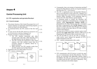
• CPU- memory communication:
(1.6)
Instructions
CPU
( Local
Memory )
Main
Memory
MM
Data
4 -2
• Consequently, there exist streams of instructions and data
between the Main Memory and the set of general registers
that forms the CPU’ s local memory.
(1.7)
• The CPU is significantly faster than the Main Memory,
that is it can read from or write in the CPU’s registers 5 to
10 times faster than it can read from or write in the Main
Memory (MM). Nowadays, VLSI technology tends to
increase the CPU/ Main Memory speeds disparity.
(1.8)
• As mentioned before to remedy this drawback, the
memory is organized in a hierarchical way; a new layer of
memory, called Superoperative Memory (SOM) is
placed between the Main Memory and CPU. At present,
the SOM is represented by the CACHE Memory (CM);
this CM is smaller and faster than MM and can be placed
wholly or in part on the same chip as CPU (the so called
internal Cache Memory).
(1.9)
• The main role of CM is to ensure a memory read or write
operation in a single clock cycle, whereas a MM access
(bypassing the CM memory) takes several clock cycles.
(1.10)
• The CM and MM are seen by the CPU as forming a
single memory space, because the operation of CM is
totally transparent to the CPU.
(1.11)
• CPU – memory communication with a cache:
(1.12)
• CPU communicates with I/O devices in much the same
way as it communicates with the Main Memory. The I/O
devices are associated with addressable registers called
I/O PORTS. The CPU can store or extract a word from
I/O PORTS (the OUTPUT and INPUT operations). This
subject is discussed in the further chapter.
(1.13)
CPU
Cache
Memory
CM
Main
Memory
MM
Data
Instructions
Data
Instructions
2. 4 -3
• The programs executed by the CPU are divided into two
broad groups: user programs and supervisor programs.
(1.14)
• A user program, known also as application program,
handles a specific application, whereas a supervisor
program manages various routine aspects of the entire
computer system on behalf of the users and it is part of
the system software named the operating system. As
examples of supervisor programs there are mentioned the
control of transferring data between Secondary Memory
and Main Memory, control of a graphic interface etc.
(1.15)
• In a normal operation any CPU switches between user
programs and supervisor programs.
(1.16)
§1.2. Flowchart of CPU operation
• It is generally useful to design CPUs that can interrupt
their current program in execution and pass to another
needed program; such requests can be received from I/O
units, the secondary memory etc. and are materialized in
interrupt signals. If accepting an Interrupt Request (IR)
the CPU suspends the execution of the current program
and transfers execution to an appropriate interrupt –
handling program (called also interrupt service routine).
(2.1)
• As interrupts need usually a fast response, the CPU must
check frequently for the presence of Interrupt Request
(IR). This happens at the beginning of any Instruction
Cycle.
(2.2)
• The mechanisms of interrupting the CPU operation will
be treated extensively later.
(2.3)
• Another special mechanism of interrupting CPU is related
to DMA implementation, where the DMA controller
takes the control of the system bus to ensure a fast
transfer of data to/from the Main Memory, without
participation of the CPU.
(2.4)
• The DMA organization and operation is presented in the
next paragraphs.
(2.5)
4 -4
• The flowchart describing roughly a CPU operation:
(2.6)
• The actions of the CPU during an Instruction Cycle are
defined by a sequence of microoperations, each of which
typically involving a register – transfer operation.
(2.7)
START
Instruction
Waiting
?
NO
FETCH PHASE
EXECUTE PHASE
Interrupt
Waiting?
NO Transfer to Interrupt
Handling Routine
YES
YES
3. 4 -5
• The time required for the shortest CPU operation
represents the CPU clock period Tclock and is a basic unit
of time for measuring CPU actions. (Tclock =
1
f
, where f
is the clock frequency measured in MHZ or GHZ).
(2.8)
• When using a Cache Memory it can be assumed that
FETCH phase requires one CPU clock cycle and
EXECUTE phase requires another CPU clock cycle.
(2.9)
§1.3. General structure of a CPU
• CPU is made up of the Control Unit ( CU ) and of the
Arithmetic and Logic Unit ( ALU ); it is also called the
processor.
CPU = ALU + CU
(3.1)
• CPU must communicate with the other units of a digital
computer: Memory Unit, Input Units and Output Units.
CPU is issuing addresses, data, control signals and is
receiving instructions, data, status signals, interrupt
requests. This communication is carried out through a
System Bus. Therefore, an obligatory component of the
CPU is an interface for the System Bus referred to as Bus
Control block (containing drivers, buffers, direction
selectors). In this way, CPU is extended with this
Interface ( IF) and becomes :
CPU = ALU + CU + IF
(3.2)
• The System Bus is formed of several subbusses each with
its particular tasks. Most important are : Address Bus,
Data Bus, Control Bus.
Address Bus is unidirectional emanating from the CPU
and reaching the Memory Unit and Input/Output Units.
Data Bus is bidirectional carrying both instructions and
data.
Control Bus is a mixed Bus containing the Control Lines,
representing commands to different units to perform
actions, as well as Status lines, representing condition
bits supplied by the external units to CPU.
(3.3)
4 -6
• Control Unit is formed of three functional blocks:
Instruction block
Address block
Control Sequencer/Control Generator block
(3.4)
• The component blocks of the Control Unit must satisfy
realisation of the following major tasks:
Extraction of the current instruction from
memory
Transferring the instruction in an Instruction
Register
Storing fields of the instruction in a Function
Register and in an Address Register.
Decoding the OPCODE and generation of the
corresponding control signals on control lines
Determination of the address of the next
instruction
Identifying the effective address of the operands
Transferring the designated operands in ALU
Performing the operation (function) provided by
the OPCODE
Storing the result
(3.5)
• The Instruction block consists of:
Program Counter ( PC )
Instruction Register ( IR )
Function Register ( FR )
OPCODE Decoder ( DEC )
(3.6)
• Program Counter is a pointer to the next instruction to
be executed; it is a register with incrementing facility and
parallel load facility.
(3.7)
• The content of the PC is used during the Fetch phase to
read the memory and to extract the instruction to be
executed by the CPU.
(3.8)
• The current fetched instruction is stored in the Instruction
Register (IR); the operation code field is transferred in the
Function Register (FR) the content of which is decoded
(interpreted) by the Function Decoder allowing
identification of the operation.
(3.9)
4. 4 -7
• The Address block consists of:
Address Register (AR) aimed at storing the logic
address contained by the address field of the
instruction in execution.
Effective address computation device, that has the
task to apply specific mechanisms for
determination of the effective address of the
operands from the logic address given in the
address field of the instruction (Addressing
techniques)
(3.10)
• Control Sequencer is a complex sequential device that
generates all commands required by the execution of the
current instruction, as well as required by the automatic
running of the program. The decision is taken based on
decoded function, on the content of the Status (Flags)
Register, on external status signals, the current phase of
the Instruction Cycle.
(3.11)
• The ALU contains a set of general registers, constituting
the local memory, aimed at storing the partial results,
operands, the processing device (implementing arithmetic
and logic operations), an Accumulator register, an
operand/buffer register, the status ( flags) register etc.
(3.12)
• The Status Register consists of a set of condition bits
representing different features associated to the generated
result (sign, carry, parity, zero etc)
(3.13)
• These blocks of the CPU are interconnected through
internal buses: internal data bus, internal address bus,
internal control/status lines.
(3.14)
• The general structure of a CPU is presented in Annex 1.
4 -8
§1.4. The evolution of CPU during the FETCH phase
• As specified previously an instruction cycle consists of
two main phases named FETCH phase and EXECUTE
phase.
(4.1)
• During FETCH phase only a part of the CPU is involved:
the Instruction block and the Control Sequencer, as seen
in the figure depicted in Annex 2.
(4.2)
• The steps of running this phase are:
1. From PC the instruction address is transferred into
MAR ( Memory Address Register ) of the
Memory Unit.
2. From Control Sequencer the command READ is
issued and after the end of transient processes
occurred in the memory, the current instruction is
extracted from the addressed location and is stored
in MBR (Memory Buffer Register ) of the
Memory Unit.
3. From MBR the instruction is transferred into the
Instruction Register (IR) of the CU, in particular
in the Instruction block, and the OPCODE field is
transferred into the Function Register..
4. The address field is transferred into the Address
Register of the Address block.
5. From the Function Register the OPCODE is
applied on the inputs of the Function Decoder
which decides the nature of the current operation.
6. PC is incremented by a command issued by the
Control Sequencer, to prepare it for the next
instruction to be fetched from the memory.
(4.3)
• Hence, at the end of the FETCH phase the content of the
PC is prepared to read the next instruction, in the Address
block, in the Address Register, it is stored the address of
the operand required for performing the current operation
(function), the Control Sequencer is ready to issue the
commands for the identified operation.
(4.4)
5. 4 -9
• From the figure depicted in Annex 2 it can be seen that
the dimension of the memory array was assumed 2k
n×
which points to the fact that an address is defined on k
bits and the operands are on n bits.
(4.5)
§1.5. The evolution of CPU during the EXECUTE phase
• The presentation assumes an arithmetic or logic operation
defined in the instruction
(5.1)
• During the EXECUTE phase it is mainly involved the
ALU, the Address block from the CU, and the Control
Sequencer, as seen in figure depicted in Annex 3.
(5.2)
• The steps of the evolution during the EXECUTE phase:
1. The Address Register supplies to the Effective
Address Calculation device the logical address that
was contained in the address field of the instruction.
In modern computers it is customary to use different
addressing techniques, so that the effective address
of the operand rarely coincides with the logical
address included in the instruction. By simple
arithmetic operations from the logical address it is
determined the effective address of the operand.
2. The effective address is sent to the Memory Unit and
stored in MAR (Memory Address Register).
3. The operand is read from the location of the memory
having the address specified by the MAR. To realize
this, Control Sequencer issues a READ command.
The operand is stored in MBR ( Memory Buffer
Register)
4. The operand is transferred in the ALU, in the
buffer/operand register. The action defined by steps
1, 2, 3 and 4 is called Fetch Data. It is assumed that
the other operand is stored in the Accumulator.
5. The processing device from ALU is performing the
operation imposed by the OPCODE, under control of
the Control Sequencer. The commands are
distributed through Control Lines.
(5.3)
4 -10
6. The result is stored in the Accumulator and the
condition bits are generated and saved in the Status
(Flag) Register. The condition bits, called also flags,
refer to different particular characteristics of the
result, like the sign, carry setting up, parity, zero
value, etc; such condition bits ( flags ) are necessary
for deciding the execution of some particular
instructions like, for instance, conditional jumps.
(5.3)
• Some instructions do not use the operand from the main
memory, instead the operand is extracted directly from a
general register that exists inside the ALU, in the local
memory. In general, there is a group of 2w
general
registers, so that it must be specified an address of the
register from the register file and by means of a register
address decoder it is identified the needed register
containing the operand.
(5.4)
• In such cases, the FETCH Data action is replaced by the
identification of the needed register from ALU, its
reading and transferring of the operand into the buffer
operand register associated to the processing device (steps
designated 2 ,3 , and 4′ ′ ′ in figure from the Annex 3.
(5.5)
• There exist variations in organization of CPUs, depending
on design criteria, adopted architecture, nature of control
unit, set of machine level instructions etc.
(5.6)
6. 4 -11
§2. Techniques for balancing the speeds of CPU and main
memory
§2.1. General considerations
• The memory system has a hierarchical structure:
secondary, main, local.
• The Main Memory contains program and data that are
currently being processed by the CPU; therefore it is
considered the “on-line” level of memory.
• There exists a great difference in capacity and speed of
operation between different levels of memory hierarchy.
(1.1)
• Computers are organized in such a way as to
automatically regulate the flow of information between
levels of memory, by software or hardware means.
• The regulation provides less frequently accessed
information being kept in slower and more capacious
memory levels, whereas more frequently accessed
information being kept into the faster and less capacious
memory levels.
(1.2)
• Main Memory is in communication with CPU, therefore
their speeds of operation would be comparable ,i.e. CPU
must get information from the Main Memory at a speed
comparable to its own operation.
(1.3)
• Speed and capacity of a memory are parameters in
conflict with each other.
(1.4)
• The ALU of the CPU is the most productive unit of a
digital computer.
(1.5)
• Special balancing techniques between CPU and Main
Memory were used to match their speeds.
(1.6)
• Balancing techniques are grouped into three categories:
a) Widening the data bus;
b) Increasing the number of levels in memory
hierarchy;
c) Prefetching the next instruction.
(1.7)
4 -12
MM
CU
ALU
Memory
Bus
CPU
§2.2. Widening the memory bus
• Programs and data to be processed are stored in the Main
Memory, as well as the results are sent back to the Main
Memory (MM), while the processing is carried out in
CPU.
(2.1)
• Connection between MM and CPU is realized through a
data bus known as the memory bus.
(2.2)
• The speed of transferring data from / into MM represents
the bottleneck of any von Neumann computer; CPU
extracts instructions and corresponding data from the MM
one at a time.
• This limitation is not technological in nature, but
architectural and is aggravated by the difference in speed
of operation between MM and CPU.
(2.3)
• This drawback was always present in digital computers
throughout their history, even nowadays, although not so
seriously as in the past.
(2.4)
• A natural solution to improve the bottleneck is to widen
the memory bus so as to extract several instructions and
data items from the MM at a time.
(2.5)
7. 4 -13
CPU
(2.6)
• Various organizations of the MM were proposed and
studied in practice. (2.7)
• The critical problem is to make MM, having the
constraint of procedural access to data, deliver a set of
instructions and data.
(2.8)
• Another problem is to decide which instructions and data
would be allowed in case of such wider data bus, when
several instructions and data are extracted from MM,
provided that the CPU operates in a procedural way, i.e.
one instruction at a time.
(2.9)
• The natural answer is to ensure that the set of extracted
instructions and transferred on the widened memory bus
represents a sequence of instructions of the program
processed by the CPU.
(2.10)
initial
CU
ALU
MM
widened
4 -14
• Then, a natural way of solving the MM organization is
division of MM on several parallel blocks (memory
modules):
(2.11)
• In such organization it is possible to have simultaneous
access to several modules, each offering an instruction or
data item.
(2.12)
• Thus, instead of having a single instruction or data
available for the CPU, now there exists a set of m
instructions or data items available for the CPU. But, the
critical problem associated to Neumann’s procedurality of
the CPU still remains – the CPU will process one
instruction at a time. Anyhow, the access time for the
instruction / data item is reduced, since a set of m such
items were read simultaneously from the m memory
blocks (modules) and inputted in the CPU via the
widened memory bus.
(2.13)
• Hence, the procedurality of memory access gives rise to
widened sets of instructions / data items, from which
CPU will take one piece at a time.
(2.14)
• A sequence of instructions / data items is not anymore
stored in locations with consecutive addresses of the MM,
but a set of n instructions / data items are stored at the
same address of the set of m blocks.
(2.15)
MM
Memory
bus
M1
M2
Mm
..
...
m n⋅ n
n
n
8. 4 -15
1α +
2α +
m+α
1++ mα
2++ mα
m2+α
(2.16)
• The efficiency depends on the probability that the entire
set of instructions in a widened word ( n m⋅ ) to be used
by the CPU; frequently, there are branches in the
program evolution that require a change of the normal
sequence of instructions. Then a new access to the block
of memories will be initiated to fulfil requirements of the
branch, before all instructions / data from the previous
word had been executed by the CPU.
(2.17)
(C.2.16.)
...
..
item 1
...
...
...
.
item m
item 2m
...
...
...
.
……
..
...
...
..
...
...
...
.
Address n n n
widened memory busmemory bus
Block 1 Block m
item m+1
item 1
item 2
item m
item m+1
item m+2
item 2m
4 -16
SM
capacity
Secondary Memory
Operative Memory
Superoperative Memory
Local Memory
ALU
CU
speed
OM
SOM
CPU
• Therefore, a model of prediction for sequences of
instructions is to be considered (beyond the scope of the
course).
(2.18)
§2.3. Increasing the number of levels in the memory
hierarchy
• The basic idea is to improve the flow from the MM to
CPU by inserting a smaller in size but very fast memory
between MM and CPU. This is referred to as
superoperative memory (at present, cache memory).
(3.1)
(3.2)
9. 4 -17
• Superoperative Memory (SOM) becomes the closest layer
of memory to the CPU. SOM becomes the “on-line”
memory for the CPU, with the main feature that SOM is
now a very fast memory.
(3.3)
• At present, SOM implementation corresponds to the
Cache Memory concept.
(3.4)
• Cache Memory is realized with very productive modules
of memory having a very low access time (units or tens of
nanoseconds).
(3.5)
• Cache Memory is delivering the current instructions and
the corresponding data to CPU at speeds that are
comparable to CPU speed.
(3.6)
• Cache Memory is exchanging blocks of information with
Operative Memory. These blocks are formed of clustered
sets of instructions and data.
(3.7)
• The organization and operation of Cache Memory is
based on the program property known as “locality”.
(3.8)
• Initially the Cache Memory is empty; when CPU calls for
the starting instruction of the program it still extracts it
from the Operative Memory, where is the entire program.
But, besides the starting instruction, the Cache Memory is
filled with an entire block of instructions /data that are
clustered around the initial instruction.
(3.9)
• It is assumed that the clustered instructions are to be
executed in sequence from the Cache Memory and not
from Operative Memory.
(3.10)
• When a failure (cache miss) of finding an instruction/data
happens, a new block of instructions /data is brought from
the Operative Memory.
(3.11)
• The strategy in designing the Cache Memory is to make
transfers between SOM and OM as infrequent as
possible. This is also based on models of prediction of
sequences of instructions and data.
(3.12)
• The transfers between SOM and OM are realized under
control of a hardware mechanism, that is transparent for
the user.
(3.13)
4 -18
• Various Cache Memory administrations were
implemented to extract the required instructions / data for
the CPU and to implement the replacement strategy
(exchanges between SOM and OM).
(3.14)
§2.4. Prefetching
• As presented previously the life cycle of any instruction
consists of two major phases:
a) the fetch phase (F);
b) the execute phase (E);
(4.1)
• Consequently, execution of a series of instructions has the
following time evolution:
(4.2)
• As it was mentioned, during the Fetch phase, it is read
the current instruction from the MM and it is decoded,
whereas during the Execute phase, the operand (data) is
fetched and the function is executed yielding the result.
(4.3)
Fetch Execute
Instruction
Cycle
F E
F E
F E
time
instruction 1
instruction 2
instruction 3
...
...
...
10. 4 -19
• The prefetching procedure consists in overlapping the
Execute phase of the current instruction with the Fetch
phase of the next instruction, provided that there are no
requests of common resources.
(4.4)
• The new time-frame of program execution becomes:
(4.5)
• It is introduced a parallelism in a time sense, in contrast to
the spatial parallelism that is characteristic to the
memory bus widening technique.
(4.6)
• Since the sequence of the processed instructions does not
depend only on the CPU but also on the instruction being
carried out (like CALL, JUMP etc.), prefetching does not
always provide the required instruction.
(4.7)
• In such particular cases the CPU will simply not utilize
the extracted and decoded instructions, but will explicitly
call for the new required instruction that has been referred
to, like in case of branching instructions.
(4.8)
• Prefetching is a simple and very efficient mechanism
frequently utilized in designing control units of the CPUs.
(4.9)
F E
F E
F E
time
instruction 1
instruction 2
instruction 3
.
...
...
...
.
4 -20
• Prefetching principle can be extended to a more detailed
refinement, by considering more steps of an Instruction
Cycle.
(4.10)
• Among the mechanisms that have been analyzed the
simplest is prefetching technique, because it exploits
some properties that inherently exist in computers,
namely the redundancy consisting in the presence of two
systems, MM and CPU, that are capable of working in
parallel.
(4.11)
• The other two techniques are more expensive, as they
necessitate new resources (Cache Memory, widened data
bus).
(4.12)
§3. An example of CPU with general registers set
organization
• It is considered an ALU with a register file containing 7
general registers R1,R2, R3,R4, R5,R6, R7. There is no
Accumulator, as in case of architectures of ALUs for
instructions with a single address (when one of the
operands is in the Accumulator).
(2.1)
• The operands, designated A and B, can be read either
from a general register R1- R7 or from the Main Memory
(MM), whereas the result can also be stored either in the
register file or sent to the Main Memory.
(2.2)
• The general structure of this kind of ALU is presented in
the figure from the Annex 4.
(2.3)
• The selection of operands A and B is done with two
specialized logical devices having the role of a selector,
called digital multiplexer. Since there are 8 potential
sources for operands there are used digital multiplexers
with 8 inputs {I0…I7}, which are selected by three
selection inputs designated 0 1 2, ,A A AAS AS AS , for
multiplexer A, and 0 1 2, ,B B BAS AS AS , for multiplexer B,
respectively.
(2.4)
11. 4 -21
• Data inputs {I1…I7}are connected to the outputs of
registers {R1….R7}, while the input I0 is dedicated to the
external input, coming from the memory (when a fetch
data from the memory is realized).
(2.5)`
• The result derived from the processing device is sent
either to one of the registers R1- R7 or to the memory. The
selection of the destination location is carried out by
means of a digital decoder with 3 address
inputs 0 1 2, ,AD AD AD and 8 outputs designated {0,1,..,7}.
The outputs (1-7) are selecting one of the registers
{R1…R7}, by enabling the LOAD operation, while the
output 0 is selecting the transfer of the result to the
memory, by enabling the vectorial AND gate.
(2.6)
• With such kind of ALU the following variants of binary
operations can be defined:
)(*)(
)(*)(
)(*)(
)(*)(
)(*)(
)(*)(
)(*)(
MMM
MRM
RRM
MMR
RMR
MRR
RRR
i
ji
D
jD
iD
jiD
←
←
←
←
←
←
←
Where:
DR is a destination register from the set
{R1…R7},
(Ri) is the content of the source register from
the set {R1…R7}
(M) is the content of a memory location
* is a general binary operator implemented in
the processing device.
(2.7)
4 -22
• The selection of the first operand is realized with the
selection vector { 0 1 2, ,A A AAS AS AS } applied on the
selection inputs S0, S1, S2 of the digital multiplexer
MUX8A, according to the following correspondence table:
A2AS 0 0 0 0 1 1 1 1
A1AS 0 0 1 1 0 0 1 1
A0AS 0 1 0 1 0 1 0 1
Selected
Source
(M) (R1) (R2) (R3) (R4) (R5) (R6) (R7)
(2.8)
• The selection of the second operand is realized with the
selection vector { 0 1 2, ,B B BAS AS AS } applied on the
selection inputs S0, S1, S2 of the digital multiplexer
MUX 8B according to the following correspondence
table:
2AS B
0 0 0 0 1 1 1 1
1AS B
0 0 1 1 0 0 1 1
0AS B
0 1 0 1 0 1 0 1
Selected
Source
(M) (R1) (R2) (R3) (R4) (R5) (R6) (R7)
(2.9)
• The selection of the destination for the result is realized
with the selection vector {AD0, AD1, AD2 } applied on
the address inputs A0 A1 A2 (where A2 is msb) of a logical
decoder DEC 3/8, with outputs 0…7. The output 0
enables the vectorial AND gate by sending the result to
memory (need of a memory WRITE cycle), whereas
outputs 1…7 are selecting as destinations the registers
R1…R7 from the register file, as specified in the next
table:
(2.10)
12. 4 -23
2AD 0 0 0 0 1 1 1 1
1AD 0 0 1 1 0 0 1 1
0AD 0 1 0 1 0 1 0 1
Selected
Destination
M R1 R2 R3 R4 R5 R6 R7
(2.10)
• The selection vectors for source and destination, SEL A,
SEL B and SEL D are sent from the Control Unit, being
generated in the Address block of the CPU.
(2.11)
• The selection of the effective operation (*) performed by
the proccesing device is realized with a function selection
vector SEL F, containing t components, which is sent
from the Control Sequencer of the Control Unit, and
defining 2t
different operations(functions).
(2.12)
• It is assumed that all registers, processing device and
local buses are on n bits; therefore, the digital
multiplexers are of vectorial type, i.e., all input and output
data are n bit vectors.
(2.13)
13. 6-1
Chapter 6
Organization of the CPU-peripheral devices
communication
§1. Peripheral devices in the computer system
• In addition to the CPU and Main Memory, any
computer system contains a set of input/output
units (I/O units).
• A powerful computer may have hundreds of
peripheral devices connected to it through
input/output units.
• Each I/O unit (module) interfaces to the system bus
and controls one or several peripheral devices.
• Examples of peripheral devices: keyboard, mouse,
video monitor, printer, plotter, scanner, hard-disk
driver, CD driver, magnetic disk driver, floppy-disk
driver, joy-stick, DVD driver, tape driver.
• Peripheral devices exhibit very large differences in
two important aspects:
in form and function, by using different
media, different principles of operation
and necessitating different sets of control
information.
in speed at which they operate, even
though the fastest ones are much slower
in manipulating information than the
CPU.
(1.1)
(1.2)
(1.3)
(1.5)
(1.4)
6-2
• Peripheral devices represent one of the main system
resources that may be shared among multiple users:
a line printer may be simultaneously needed by
several processes, although they must use it
sequentially and a rule of serving has to be
established.
• The peripheral devices together with I/O units are
forming the I/O architecture of the computer system.
• The I/O architecture represents the interface to the
outside world of a digital computer.
• The external devices can broadly be classified in the
following groups:
1. human readable, that is suitable for
communicating with the user.
2. machine readable, that is suitable for
communicating with equipment.
3. communicating with remote devices,
interchanging data with other computers.
• In a simplified analysis any peripheral device has the
following structure:
(1.6)
(1.7)
(1.8)
Control logic Transducer
Data Buffer
Data bits to/from I/O units
Control signals
from I/O unit
Status signals
to I/O unit
Specific Data to/from
environment
(1.9)
14. 6-3
where:
• Control signals determine the function that the
device will perform.
• Status signals indicate the state of the device.
• Data are in the form of a set of bits to be sent to
or received from the I/O unit.
• Control Logic associated with the device controls
the device operation in accordance with the commands
issued by the I/O unit and the type of peripheral device.
• Transducer converts data from the electrical to other
forms of energy during output operation and from
other forms to electrical during the input operation.
• Typically a buffer has to be associated with the
Transducer to temporarily hold data being transferred
between I/O units and the external environment.
§2. Input/Output units.
• The generic model for an I/O unit is presented below:
Address lines
Data lines
Control lines
I/O unit
System
Bus
……..
(P1)(P2)(P3) (Pn)
Lines to
peripheral
devices
(2.1)
(1.10)
6-4
• An I/O unit (module) is not simply a set of
mechanical connectors that wire a peripheral device
into the system bus; it contains some “intelligence”
materialized in some logic for performing a
communication function between the peripheral
device and the system bus.
• The necessity of I/O units is given by the following
reasons:
1. there is a wide variety of peripherals with
various methods of operation; therefore,
it is impractical to incorporate the necessary
logic within the CPU to control all devices.
2. the data transfer rate of peripherals is much
slower than that of the CPU and memory.
Thus, it is totally impractical to use the high
speed system bus to communicate directly
with peripheral devices.
3. peripherals often use different data formats
and word lengths than the CPU to which
they are attached.
• Any I/O unit has two major functions:
1. interface to the CPU and memory via the
system bus.
2. interface to one or more peripheral devices.
• The major I/O requirements are:
1. Control unit and timing.
2. CPU communication.
3. Peripheral device communication
4. Data buffering
5. Error detection.
• The CPU may communicate with one or more
peripheral devices in unpredictable schemes,
depending on the program’s need for Input/Output.
(2.2)
(2.3)
(2.4)
(2.5)
(2.6)
15. 6-5
• In standard organization the system bus must be
shared among many activities, including I/O activity.
• Description of a transfer of data item from a
peripheral device to CPU:
1. CPU interrogates the I/O unit to check the status
of the device.
2. The I/O unit returns the device status to CPU.
3. If the device is operational and ready to transmit,
CPU requests the transfer of data item by means
of a command sent to the I/O unit.
4. The I/O unit obtains the data item (8,16,24 bits)
from the device.
5. The data item is transferred from the I/O unit
to the CPU.
• Each of the interactions between the CPU and I/O
unit involves one or more bus arbitration.
• I/O units vary considerably in complexity and the
number of peripheral devices they control.
• The general structure of an I/O unit would be as follows:
• Each I/O unit must have a unique address.
• If an I/O unit allows connection of several devices,
then each device has its own address, so that the I/O
unit must be able to recognize and generate
addresses of all devices it controls.
Data registers
Status/Control
registers
I/O
Logic
Ext.
device
interface
logic
Ext.
device
interface
logic
Data
Status
Control
Data
Status
.....
Data
lines
Address lines
Control lines
CPU
Peripheral
device
Control
(2.7)
(2.8)
(2.9)
(2.10)
(2.11)
(2.11)
6-6
• Data transfers to and from the I/O units are buffered
in one or several data registers.
• There must be one or several status registers that
provide current status information.
• A status register may function also as a control
register to accept detailed control information from
the CPU.
• CPU uses control lines to transmit commands to the
I/O units.
• In its simplest form, the I/O unit leaves much of the
work of controlling a device to the CPU.
• I/O unit and the CPU communication assumes the
following actions:
1. Command decoding – I/O unit accepts
commands from the CPU, signals that are sent
on Control bus.
2. Exchange of data – carried out over the Data bus.
3. Status reporting – because peripherals are slow
it is important to know their status through the
I/O unit. Common status signals are BUSY,
READY, etc
4. Address recognition – each device must have
a unique address so that I/O unit must recognize
the unique address for each peripheral it controls.
(2.12)
(2.13)
(2.14)
(2.15)
(2.16)
(2.17)
16. 6-7
§3. Modes of transfer
• Data transfer between the CPU and peripheral devices
is handled in one of the following 3 possible modes
( I/O techniques) :
1. Data transfer under program control or
programmed I/O
2. Interrupt initiated data transfer(interrupt
driven I/O)
3. Direct Memory Access (DMA) transfer
• Program-controlled transfers are the result of
I/O instructions written in the computer program
which is in progress. Each transfer is initiated by
an instruction in the program. As ascertained before,
each transfer is between a register of CPU (for
instance, the Accumulator) and the peripheral device,
or between a register of CPU and the memory.
Transferring data under program control
requires constant monitoring of the peripheral device
by the CPU to identify when a transfer can again be
carried out.
In the program-controlled transfer, the CPU stays in
a program loop until the I/O unit indicates that it is
ready.
This is a time consuming process since it
keeps the CPU busy needlessly.
(3.1)
(3.2)
(3.3)
(3.4)
(3.5)
6-8
• In case of interrupt-driven I/O it is used the
interrupt facility of the CPU. When running a
program, an I/O instruction informs the I/O unit to
issue an Interrupt Request when the peripheral
device becomes available. After that the CPU
switches to another program, while the I/O unit
watches the peripheral device. When the device is
ready for data transfer, it generates an interrupt
request to the CPU. Upon detecting this request the
CPU stops momentarily the task it is doing, branches
to a service routine to process the data transfer and
then returns to the task it was performing.
• In DMA, the dedicated I/O unit, called DMA
Controller, transfers data into or from the Memory
Unit through the memory bus. The CPU initiates this
type of transfer by supplying the starting memory
address and the number of words to be transferred
and then frees the bus by rising its terminals in (Z)
state. The DMA controller takes control of the bus
and realizes the transfer. After that it issues an
interrupt request to CPU to indicate that the transfer
ended. The DMA controller frees the bus and CPU
regains control of the bus. There are possible other
more sophisticated mechanisms of DMA, known as
stealing a memory cycle from the CPU.
§4. I/O Processors (channels)
• It was seen that I/O operations are time-consuming;
in the classical von Neumann organization these
operations reduce drastically the throughput of any
CPU
• It would be useful if the overlapping of the CPU
activity with I/O units activity would have been
possible, in order to parallelize their activities.
(3.6)
(4.1)
(4.2)
(3.7)
17. 6-9
• By natural evolution of the I/O units, they were
transformed from simple controllers into I/O
processors or I/O channels.
• The I/O unit was enhanced to become an I/O
processor in its own right, with a specialized
instruction set tailored for I/O operations. The CPU
directs the I/O processor to execute an I/O program
that is placed in memory.
• The I/O processor fetches and executes these
instructions without CPU intervention. This allows
the CPU to continue its main task, that of making
computations and not manipulating a slow I/O
operation.
• CPU has to specify to the I/O processor what kind of
I/O operation is to be run and after that it will be
interrupted only when the entire sequence has been
performed.
• I/O processor has its own local memory, its own
ALU and control unit.
• I/O processor can control a large set of I/O devices
with minimal CPU involvement.
(4.3)
(4.4)
(4.5)
(4.6)
(4.7)
(4.8)
6-10
• The already presented general structure of a digital
computer can be enhanced by including I/O
processors :
• Thus, CPU is relieved of I/O related tasks and
improves its performance.
Input
peripheral
devices
Secondary
Memory
I/O Processor
Main
Memory
ALU
Control Unit
I/O
Processor
I/O
Processor
Output
peripheral
devices
CPU
Data
Programs
status information
control information
flow of data
instructions stream
Results
Instructions
(4.9)
(4.10)
18. 6-11
• I/O processor has the ability to execute I/O
instructions which gives it the complete control over
I/O operations. CPU initiates an I/O transfer by
instructing the I/O processor to execute a certain
program which specifies the device involved in
operation, the area of memory for storage, priority,
and actions to be undertaken for error conditions
situation. The I/O processor follows these instructions
and controls the data transfer to/from peripheral
device.
• Computer systems are containing a hierarchy of
processors, where the prime role is assigned to the
CPU.
§5. Selector and multiplexer I/O Processors (Channels)
• Two types of I/O processors are known in computer
system
(1) selector
(2) multiplexer
• The selector channel controls multiple high-speed
devices and, at any time is dedicated to the transfer
of data with one of those devices.
Thus, the I/O selector channel selects one device
and caries out the data transfer.
• A multiplexer channel can handle I/O operations
with multiple low speed devices and medium speed
devices at the same time,based on time slicing
principle. Depending on the peripheral devices
speed of operation the following two types of
organizing the transfers can be identified:
(4.11)
(5.1)
(5.2)
(5.3)
6-12
Byte multiplexer – when for a time slice
only a byte ( word ) is transferred; this is
applied in case of very slow peripheral
devices.
Block multiplexer – when for a time slice a
block of bytes (words ) is transferred; this is
applied in case of faster peripheral devices.
• As it was mentioned, to each I/O processor there are
connected several devices through an I/O controller
having two sections : logical interface (IF) and
device controller ( K ) :
• The logical interface is manipulating digital
information, whereas the device controller is
manipulating signals specific to the physical
nature of the peripheral device.
• The entire I/O architecture consisting of selector
channels and multiplexer channels can be represented
as in Annex 6.
• In general, CPU – Channel (I/O P) communication
may take different forms depending on the particular
computer system.
(5.8)
• Any modern computer system has several channels; a
channel performs extensive error detection and
correction, data formatting, code conversion etc. The
channel can interrupt the CPU under any error
condition.
(5.9)
I/O processor Peripheral
Device
K
Device
Controller
IF
Logical
Interface
(5.4)
(5.5)
(5.6)
(5.7)
19. 6-13
• The shared Main Memory stores the CPU and
Channel programs and contains a CPU/Channel
Communication area. This common area is used for
passing information between the two processors
(CPU and Channel) in form of messages.
(5.10)
• The messages refer to
device addresses
memory buffer addresses for data
transfer
types and modes of transfer
address of channel program
status of channel
(5.11)
• While initiating an I/O transfer, the CPU firstly
checks the status of the channel to make sure that the
channel is available. It then places the Control Words
into the communication area.
(5.12)
• The CPU issues the START I/O signal to enable the
I/O operation.
(5.13)
• The channel gathers the I/O parameters, executes the
appropriate channel program, transfers data between
devices (if requested) or into/from the Main Memory
by acquiring the memory bus (using bus arbitration
protocol).
(5.14)
• The CPU can continue its activity with another
program while the channel (I/O P) is busy with the
I/O program.
(5.15)
• Once the transfer is complete, the channel sends an
Interrupt Request to the CPU through DONE I/O line
(5.16)
• The CPU responds to the interrupt by issuing the
instruction to read the status word from the channel;
the channel responds to the instruction by placing the
contents of its status report into the memory location
specified by the memory address field in the
instruction.
(5.17)
• The status word indicates whether the transfer has
been completed by the channel or if any errors
occurred during the transfer.
(5.18)
6-14