Download as PDF, PPTX

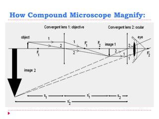
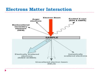

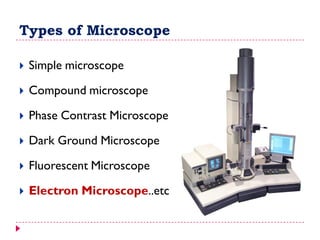
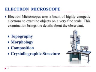
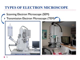
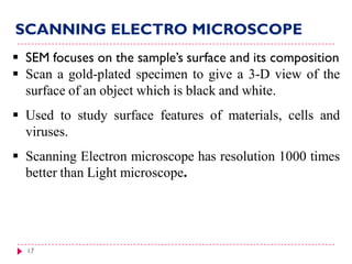
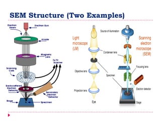
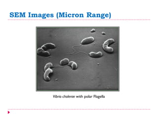

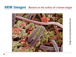
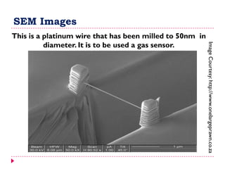
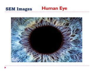
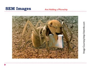
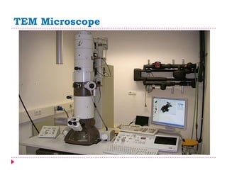
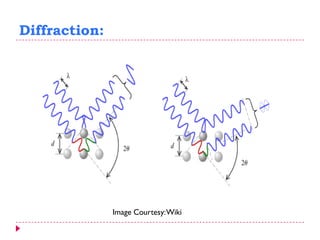
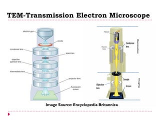
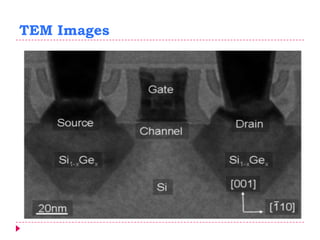
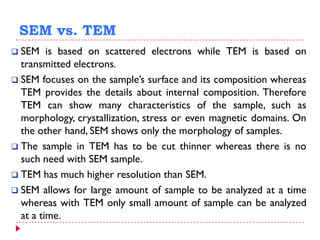
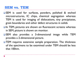


This document provides an overview of electron microscopy techniques. It begins with a brief history of microscopy and an introduction to electron microscopes. It describes two main types: scanning electron microscopes (SEM) which scan the surface of samples to create 3D images, and transmission electron microscopes (TEM) which use transmitted electrons to reveal internal structure of thin samples. SEM typically provides lower magnification but allows viewing of larger sample areas, while TEM provides higher resolution down to the atomic scale but requires thinner sample preparation. Examples of images from each microscope are shown and their applications and differences are summarized. More advanced scanning probe microscopes are also mentioned.


