This document discusses the advantages and disadvantages of flip-chip technology, particularly C4 flip-chip bonding compared to traditional wire bonding techniques in integrated circuit packaging. Flip-chip designs enhance I/O density, reduce simultaneous switching noise, and improve thermal stability but face challenges such as alpha particle emission and the need for updated design tools. The document also outlines various design flows and methodologies for implementing flip-chip technology in electronic circuits.
Introduction to flip-chip technology, its methodologies, and increased I/O possibilities compared to traditional designs.
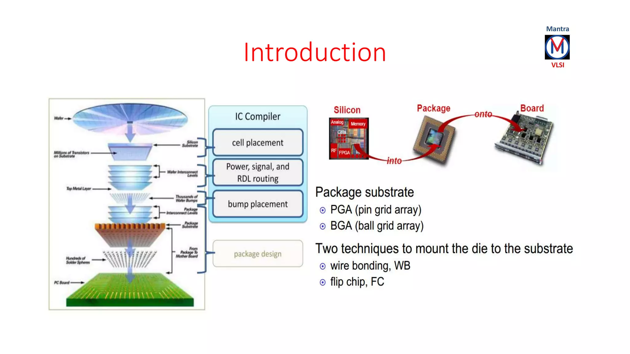
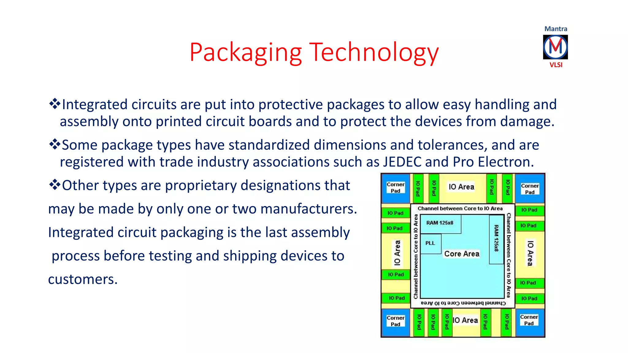
Overview of IC packaging methods aimed at protecting devices during assembly and shipment.
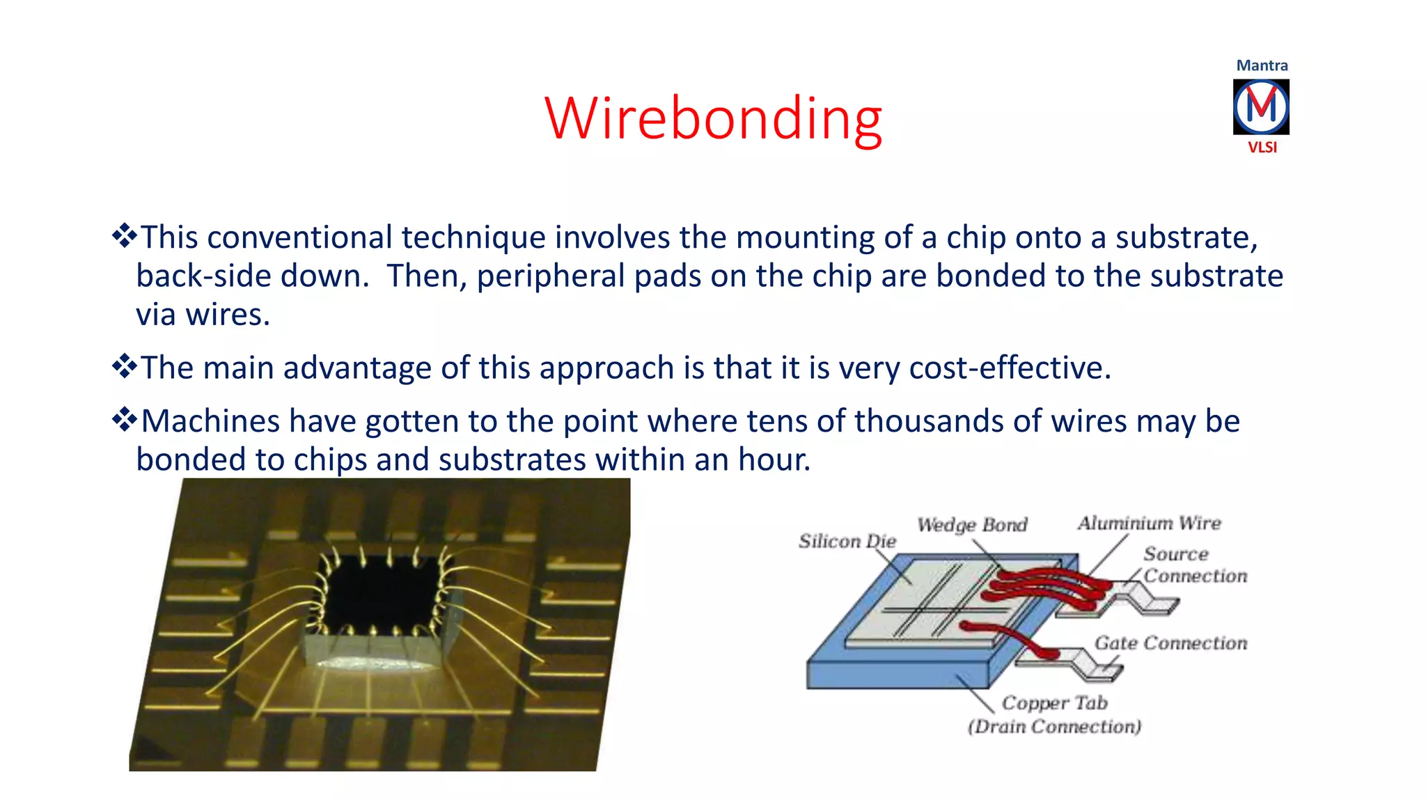
Description of wirebonding as a cost-effective interconnection method and its limitations related to design flexibility and performance.
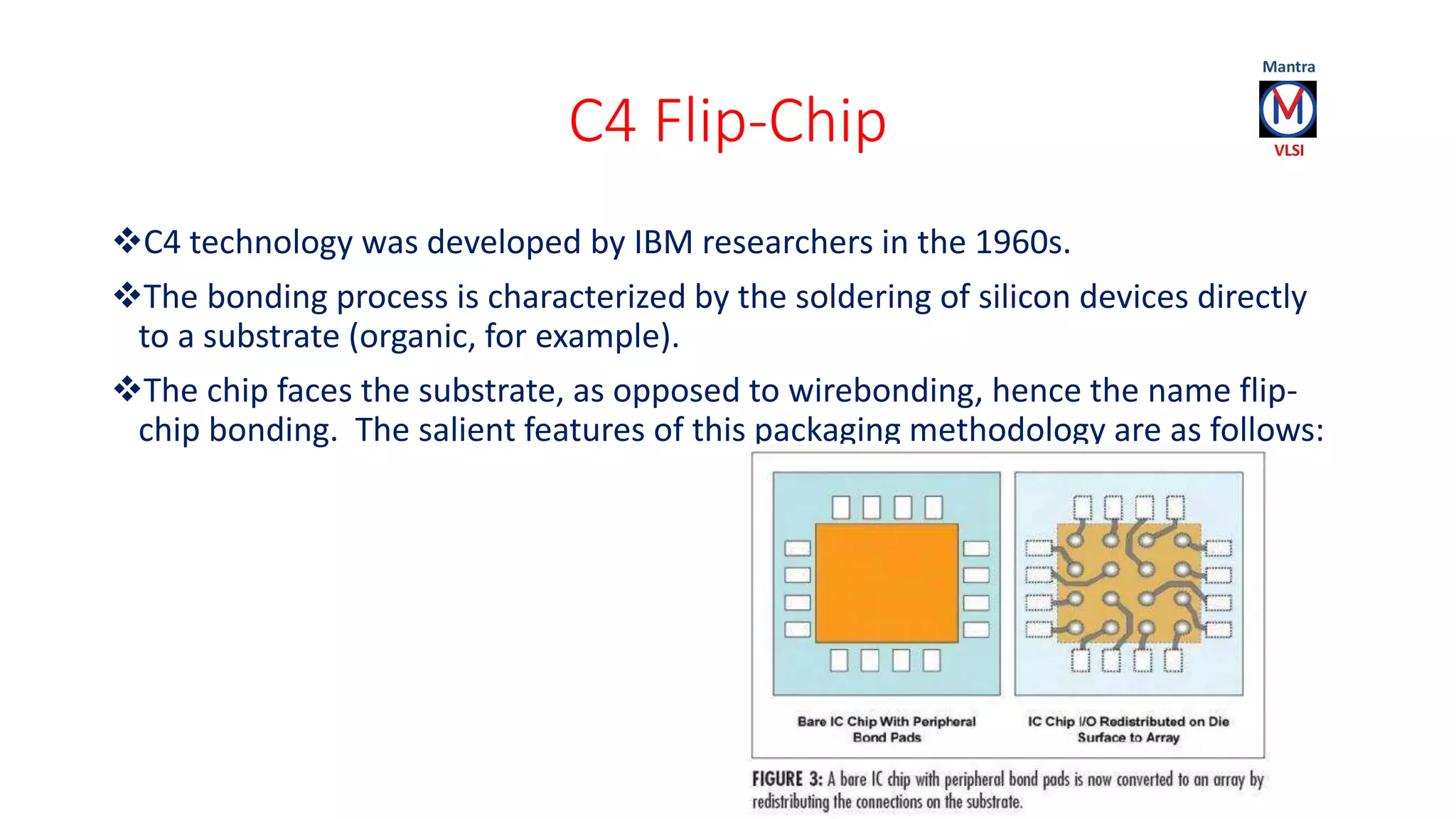
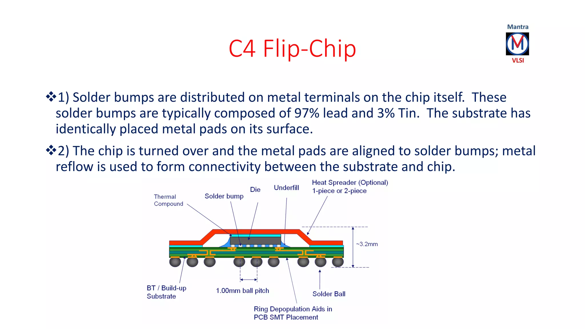
Overview of C4 flip-chip technology, its advantages such as increased I/O density, and drawbacks associated with solder bump materials.
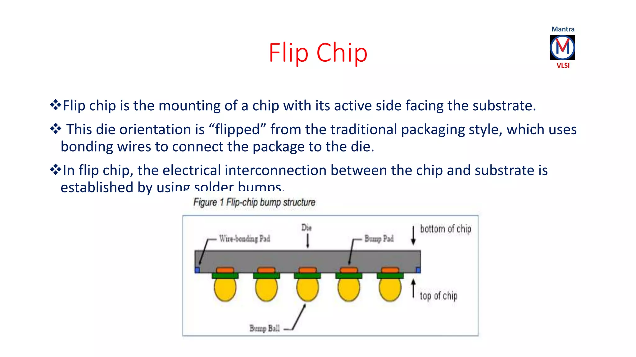
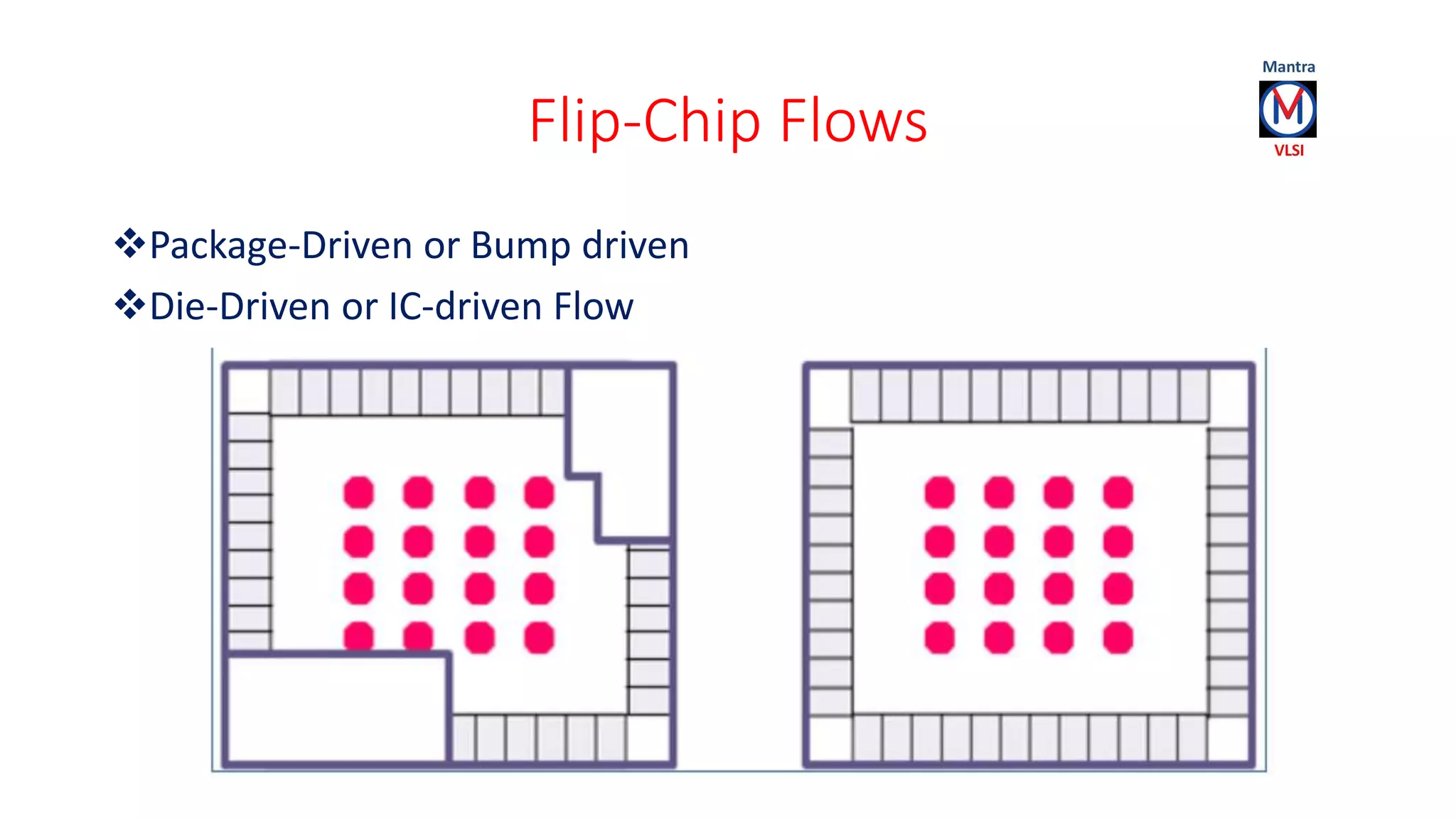
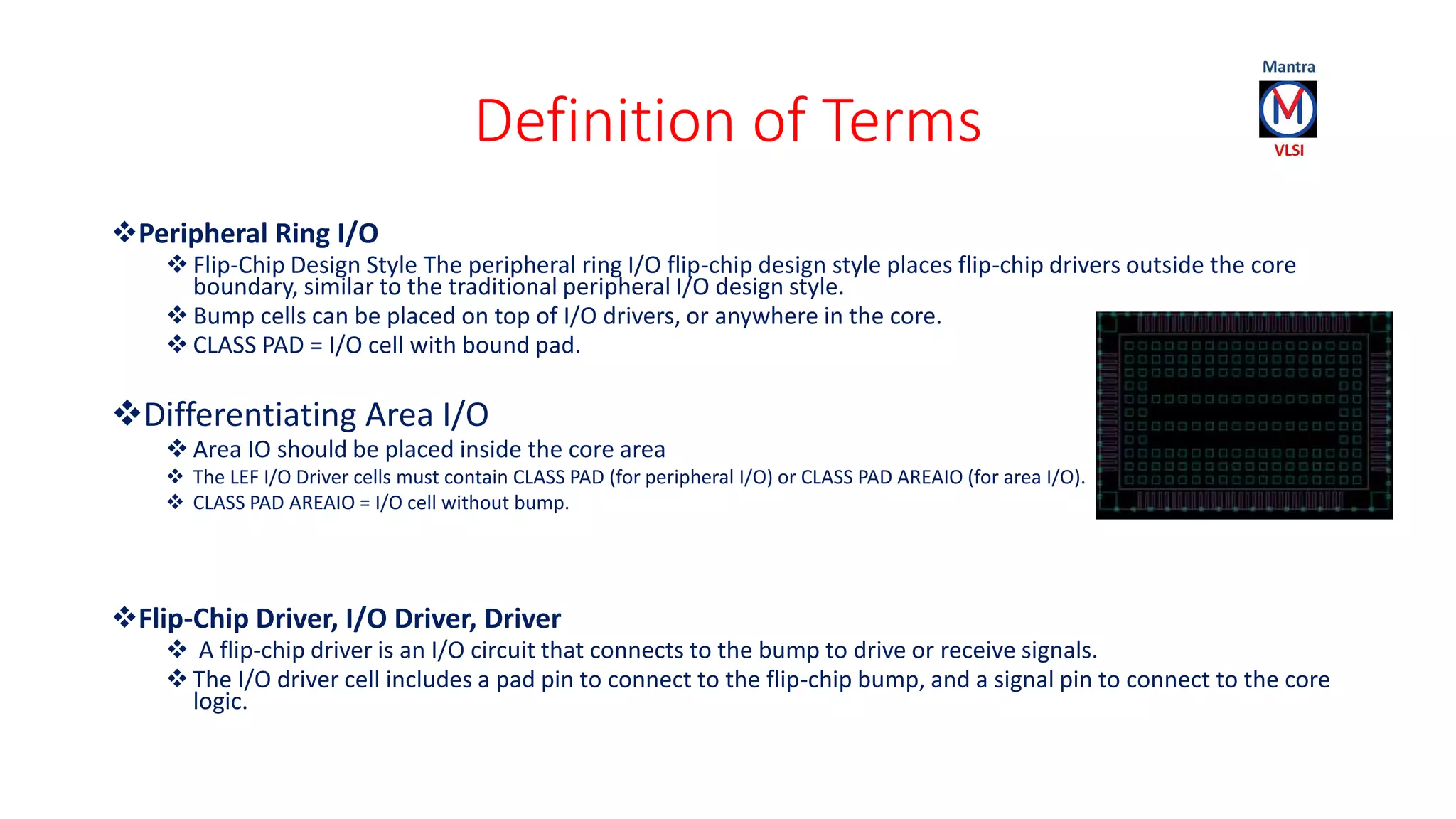
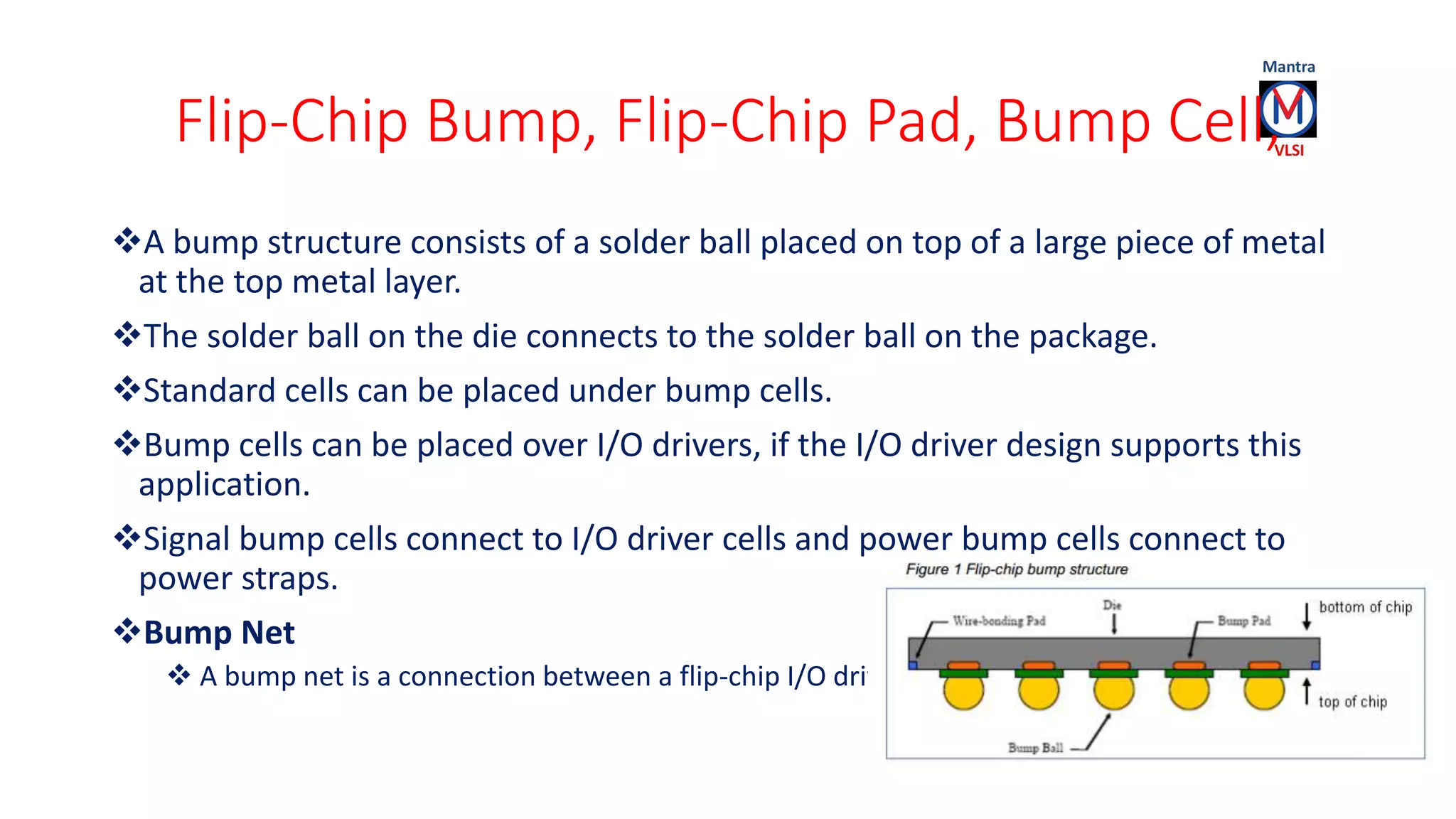
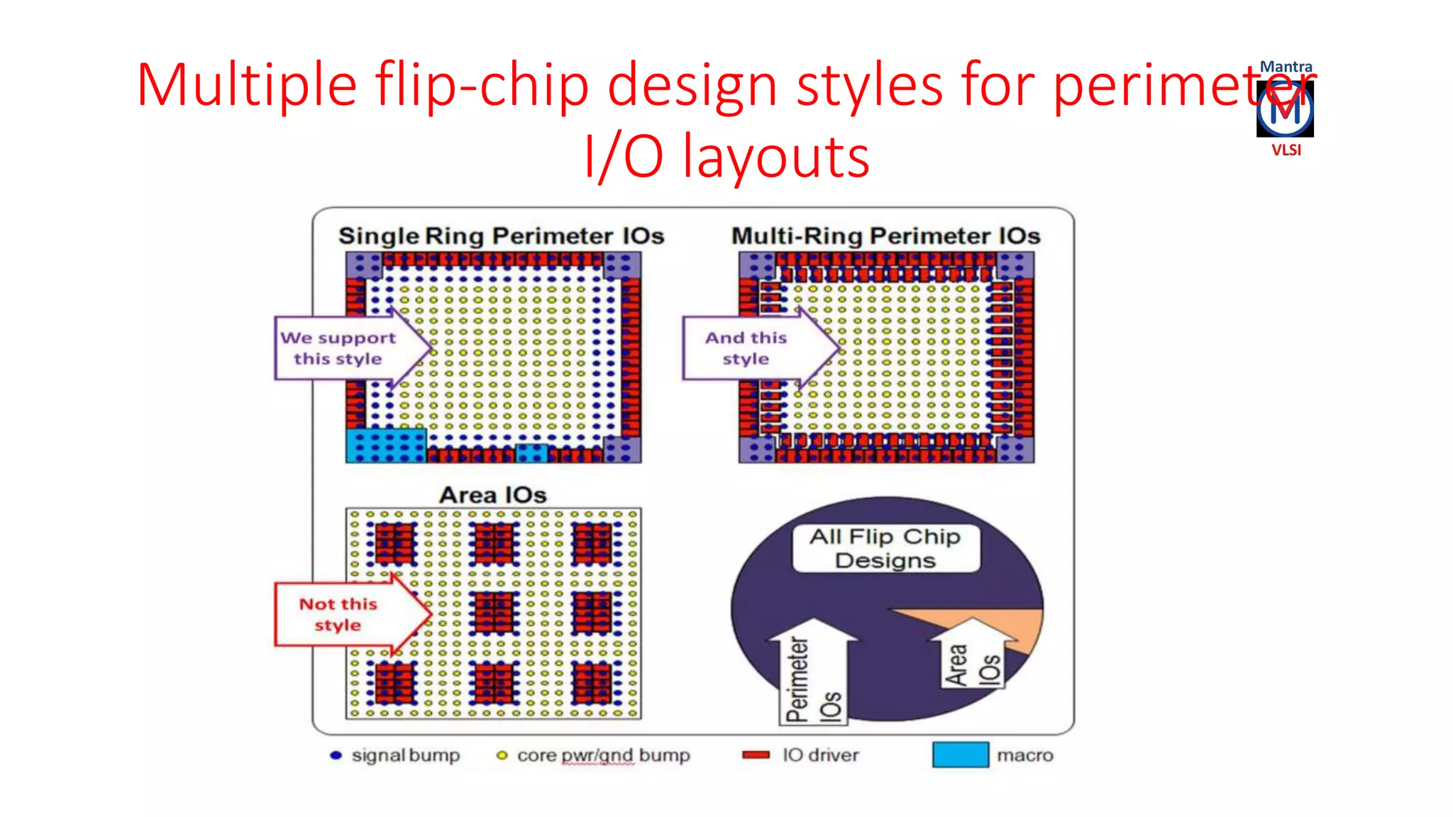
Definition and explanation of flip-chip design styles, including peripheral ring I/O and bump cells.Definitions of key terms related to flip-chip designs, including bump structures and signal connections.
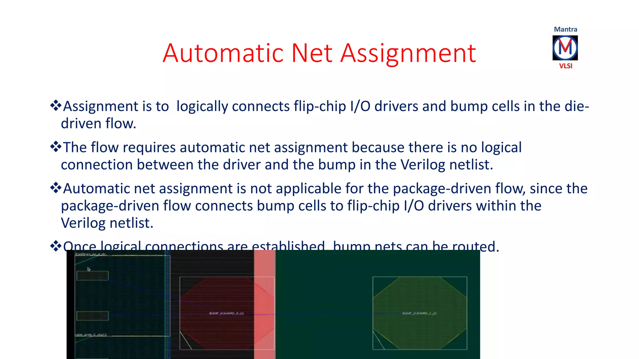
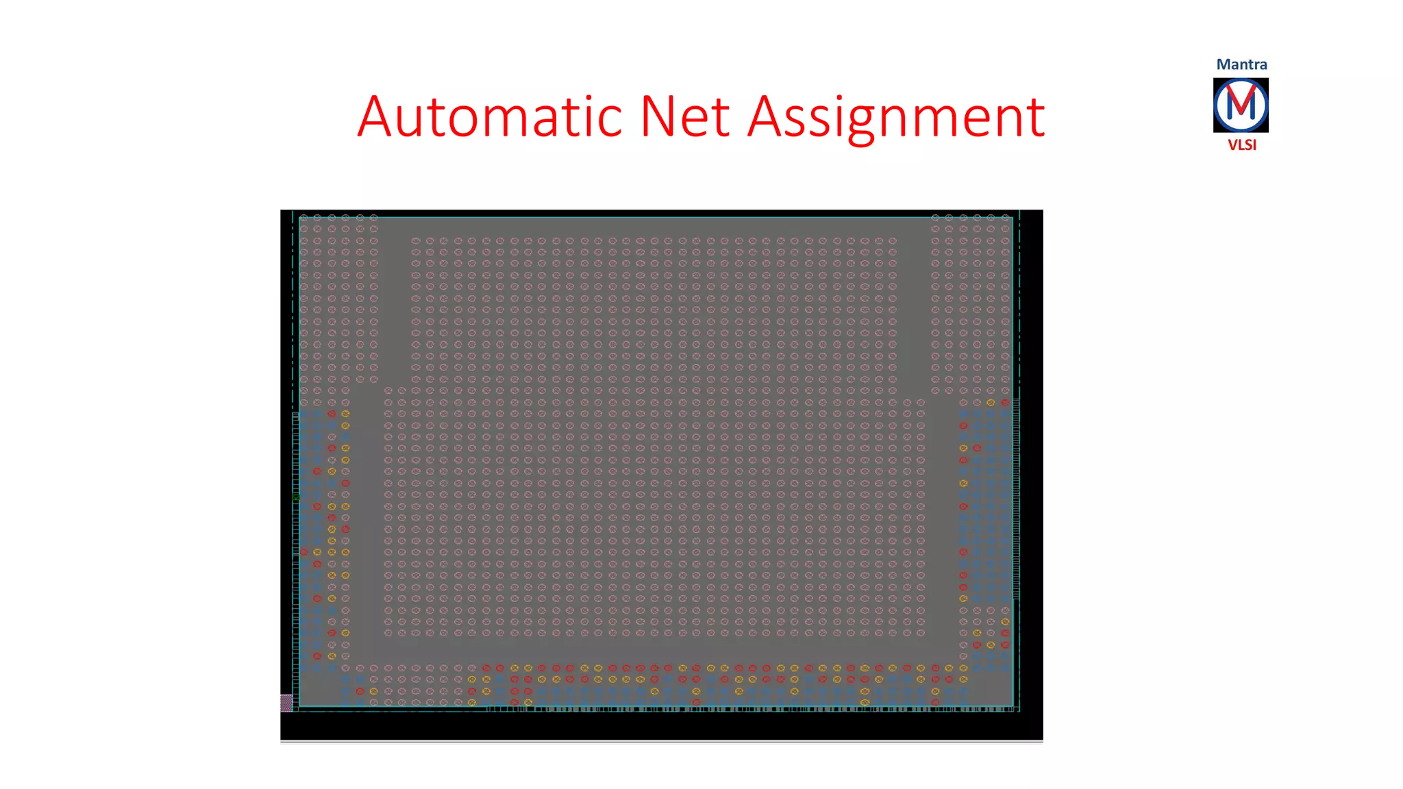
Discussion on the process of automatic net assignment for driver connections in flip-chip designs.
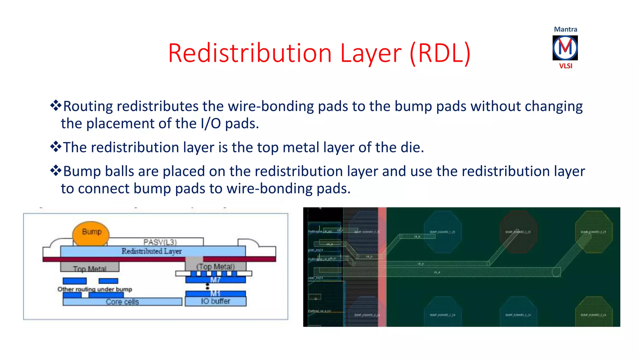
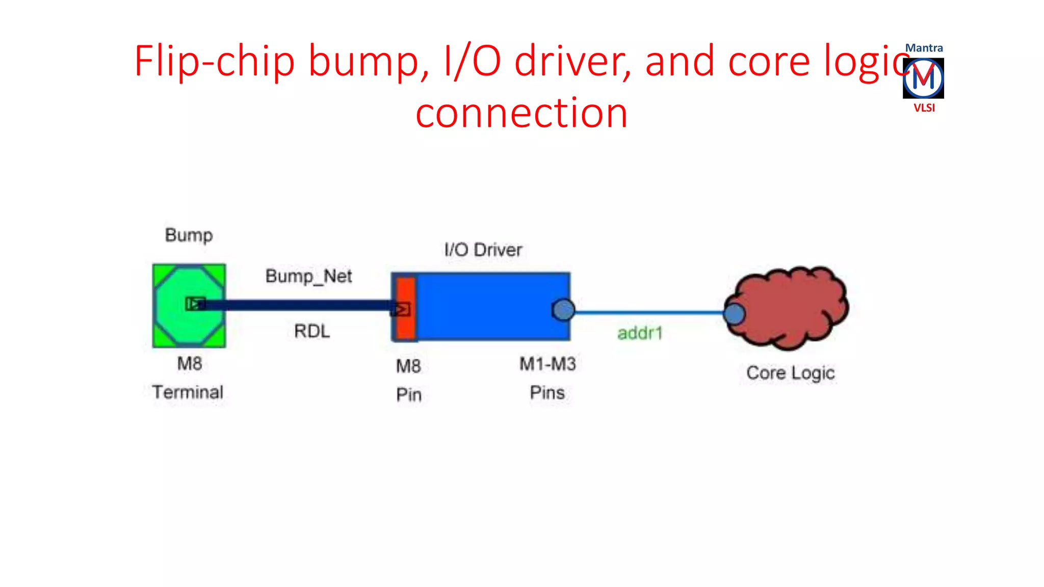
Explains the function of the redistribution layer in connecting bump pads to wire-bonding pads.
An overview of connections between flip-chip bumps, I/O drivers, and core logic.
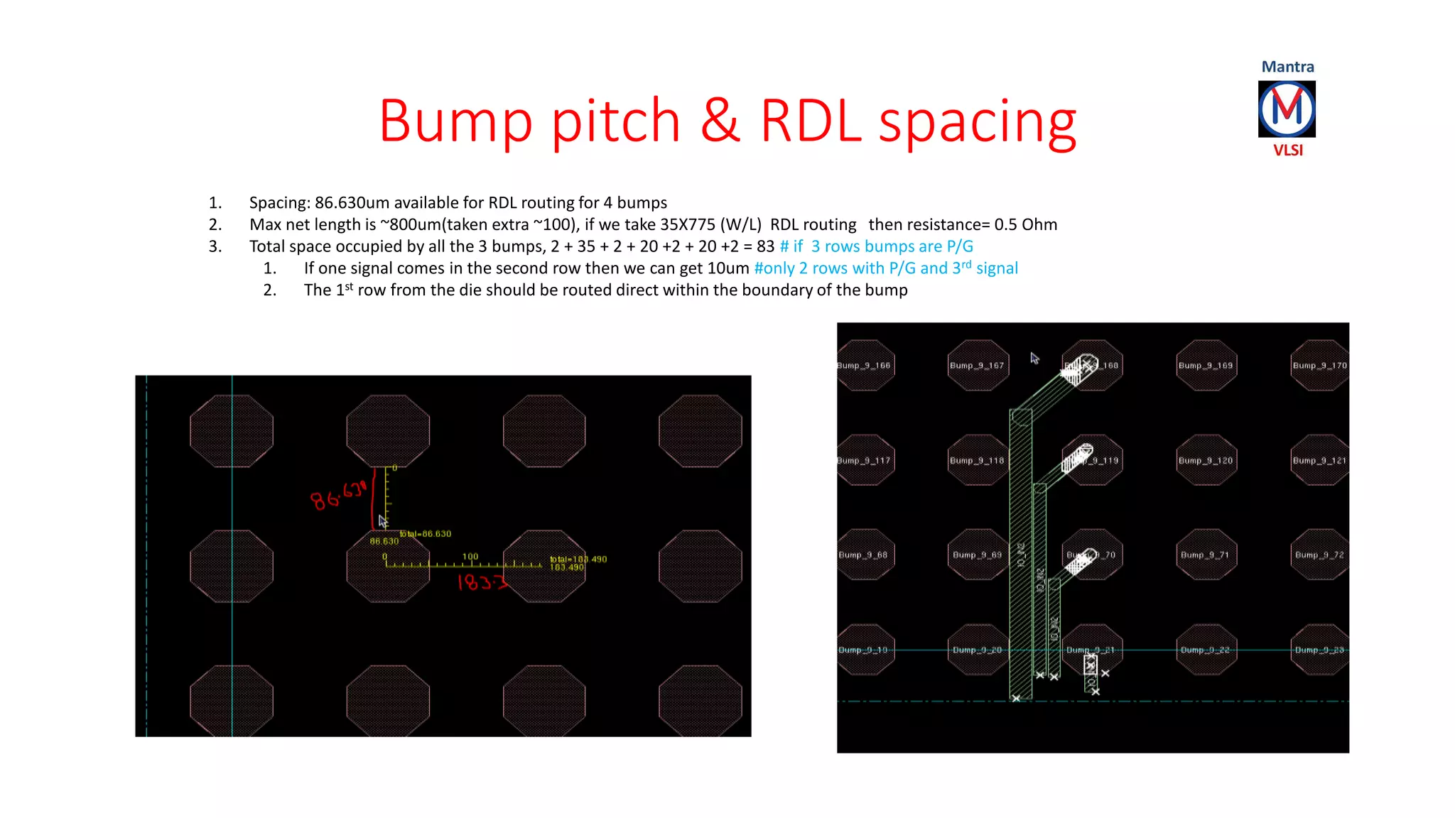
Details on bump spacing and net lengths in flip-chip designs, with specific measurements provided.
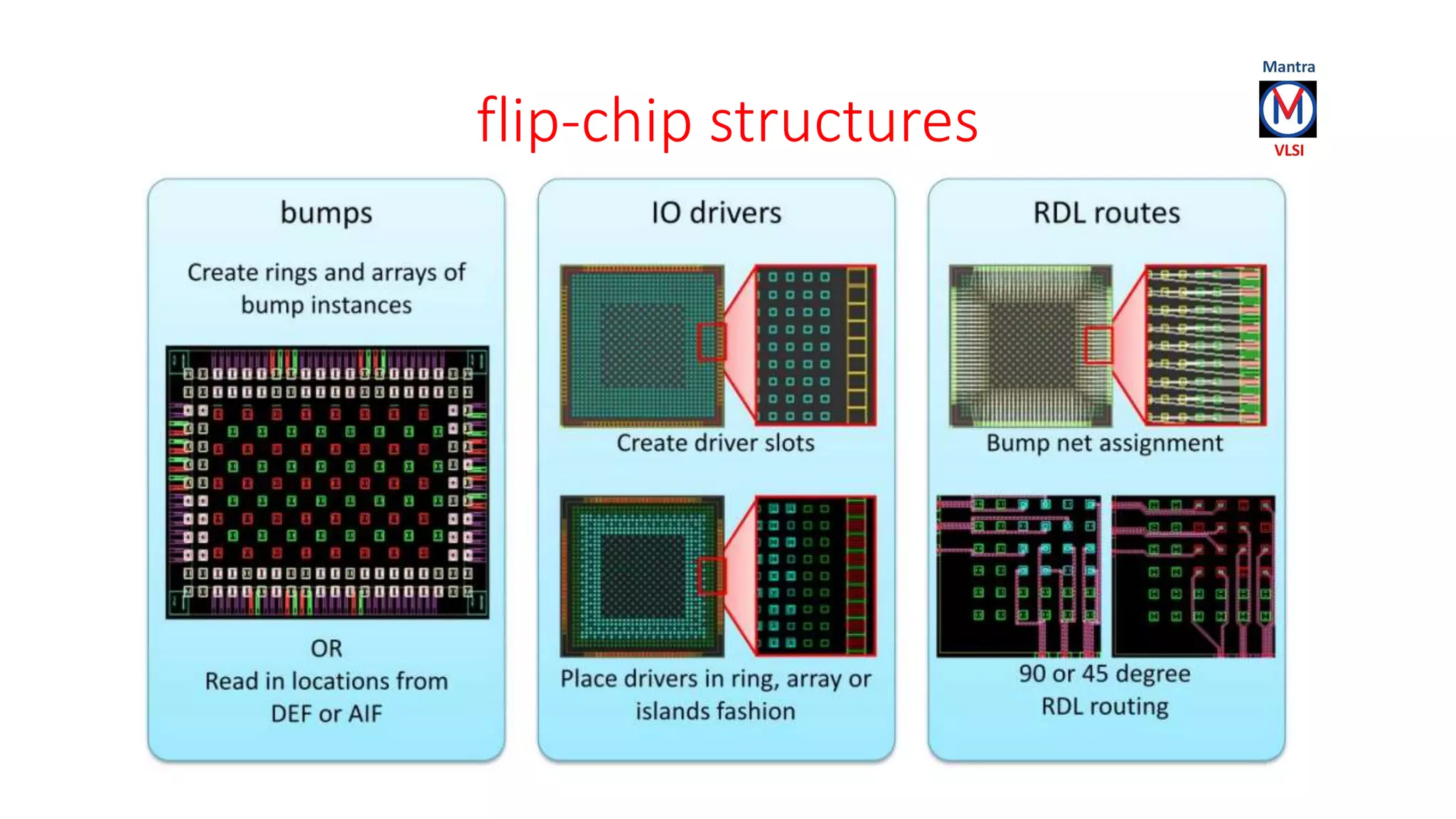
Different structural designs available for flip-chip configurations and their layouts.
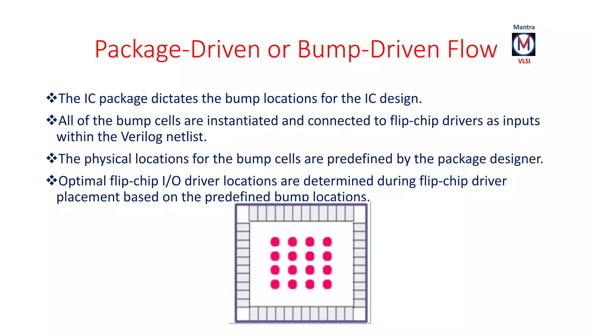
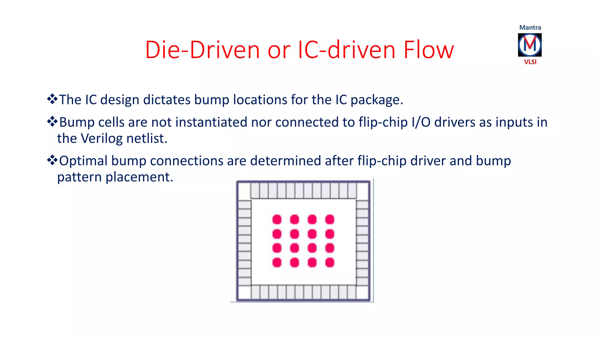
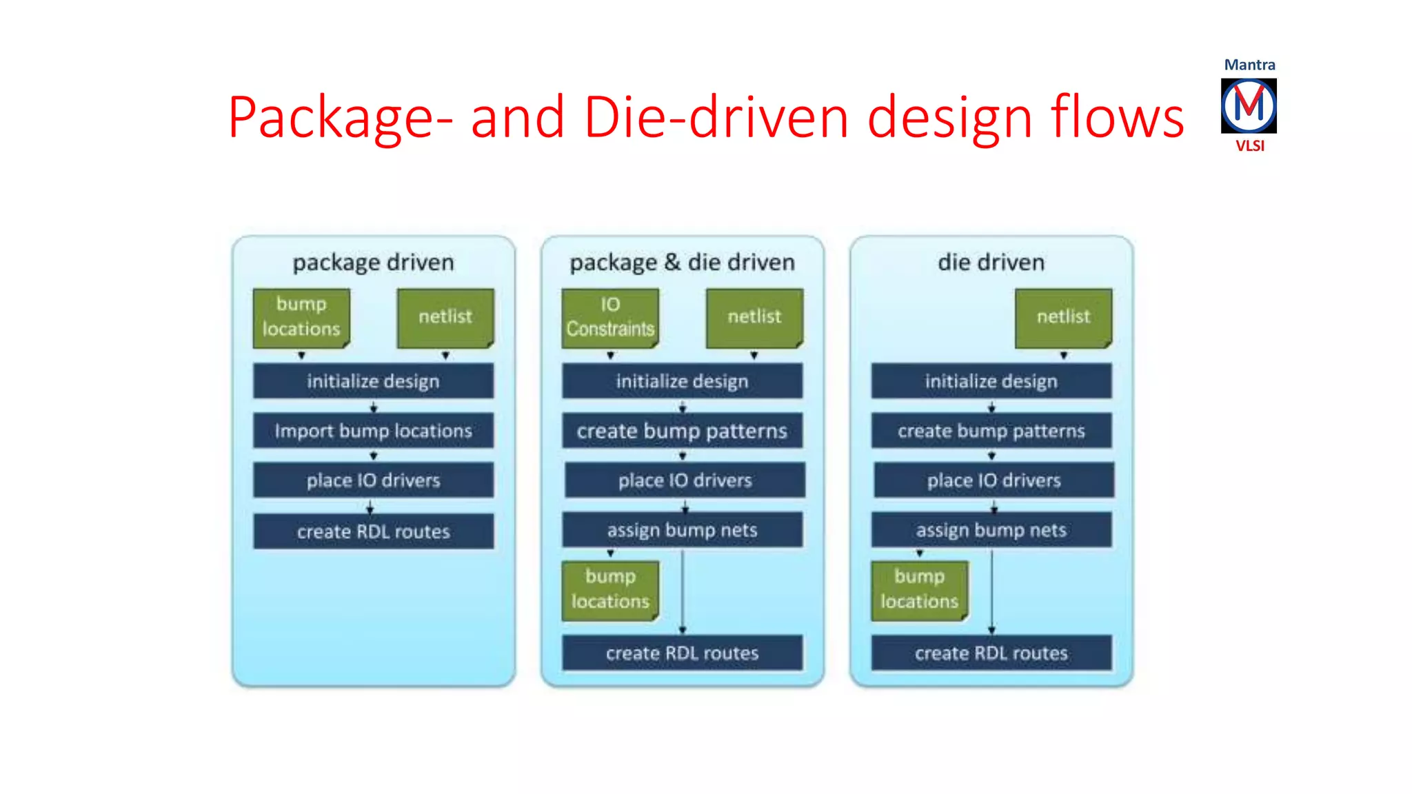
Reiterating the distinctions between package-driven and die-driven design methodologies.
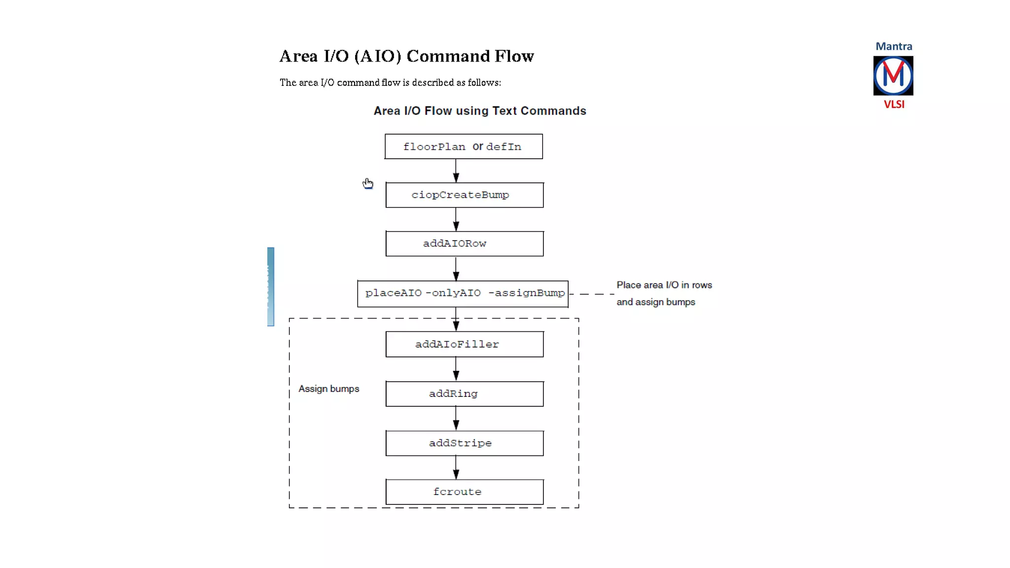
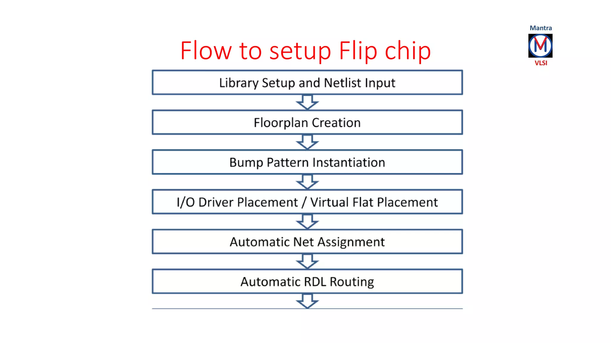
Overview of the necessary steps required to establish a flip-chip design flow.
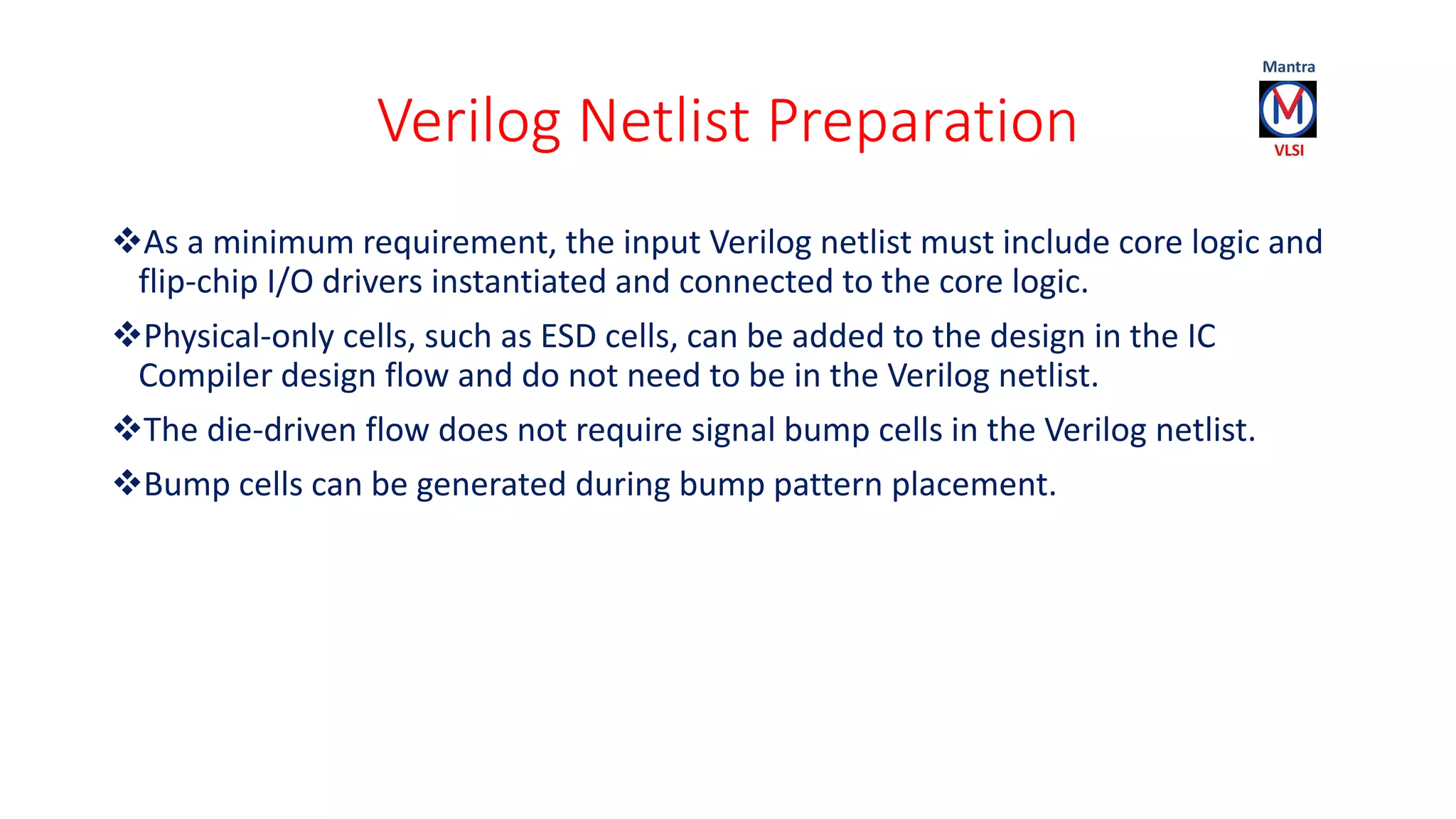
Preparation steps for Verilog netlist requirements in flip-chip design, focusing on core logic connections.
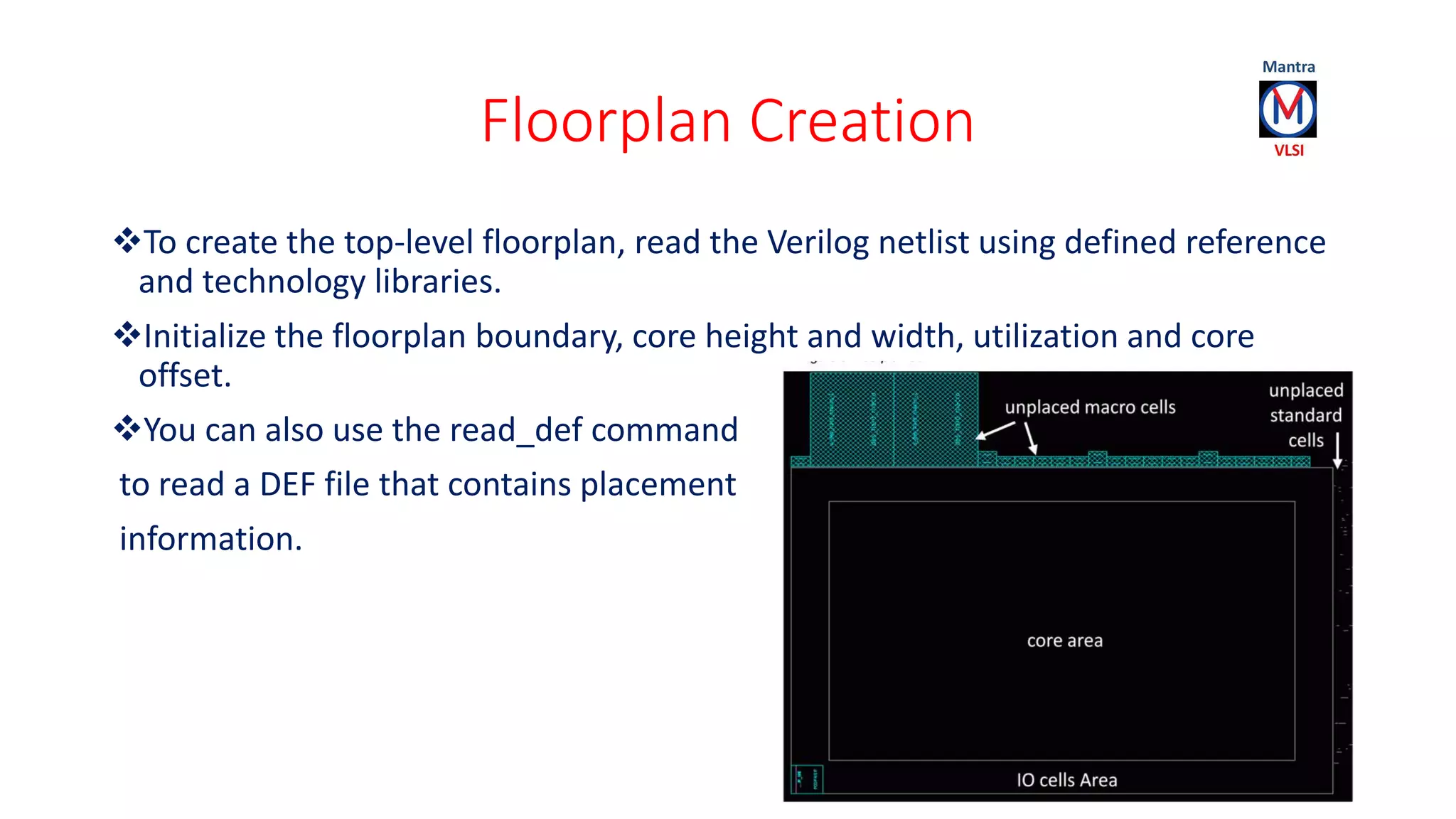
Guidelines for creating the top-level floorplan of flip-chip designs based on defined inputs.
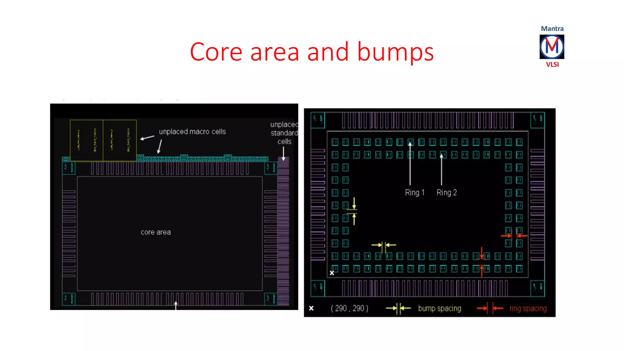
Discussion on the spatial relationships between the core area and bump placements in designs.
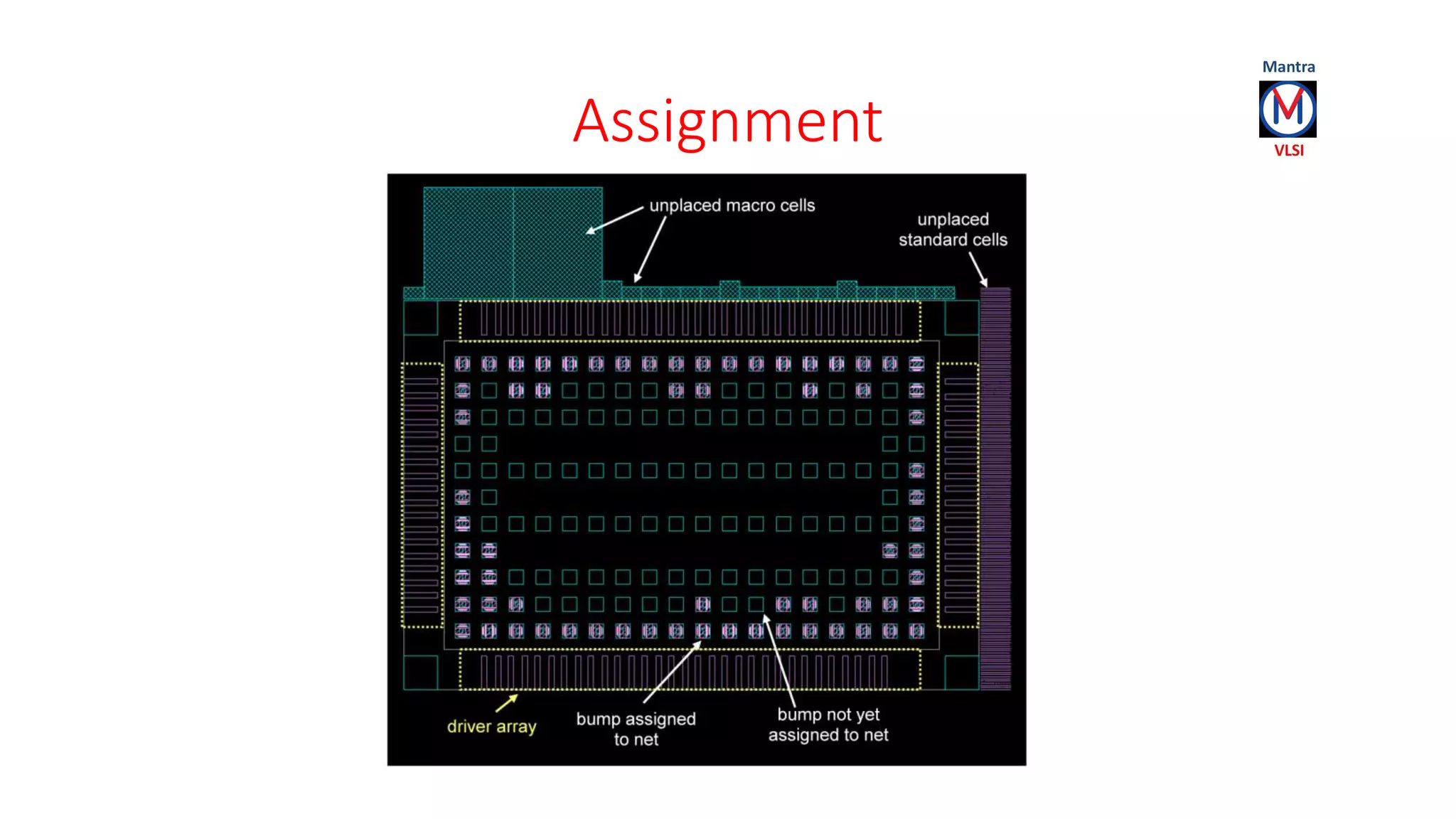
General assignment processes within flip-chip designs.
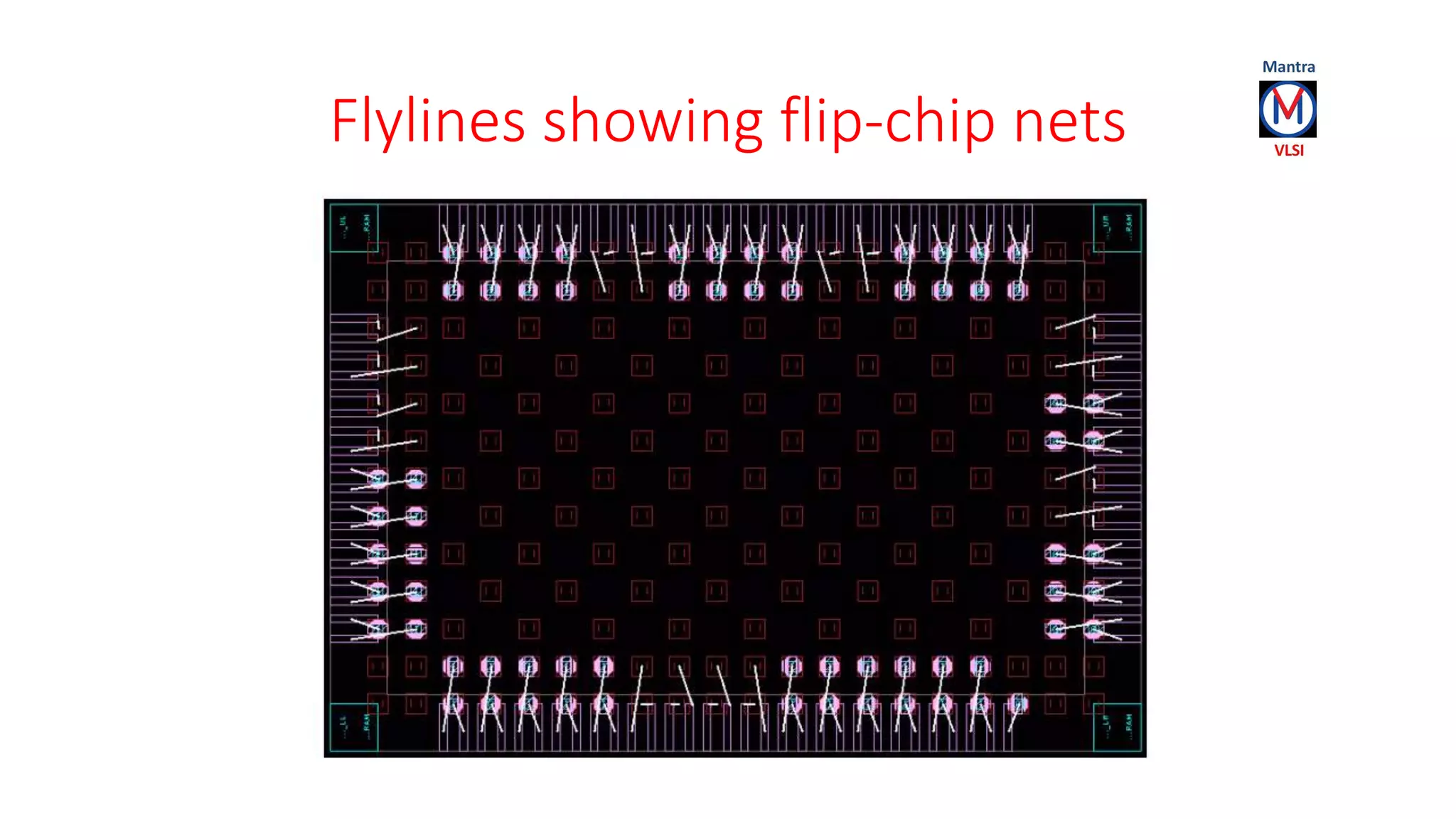
Visualization elements related to the connectivity of flip-chip nets.
Routing strategies for bump nets in flip-chip configurations.
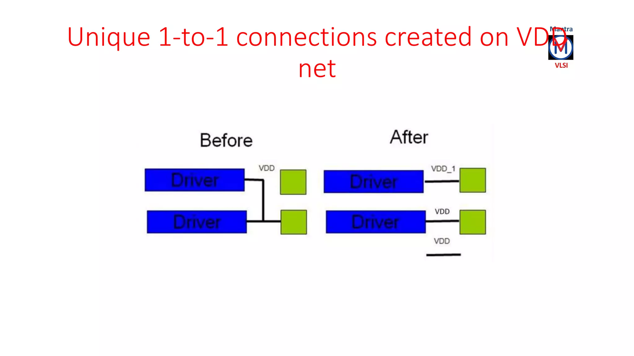
Emphasis on unique connections created for power distribution in flip-chip designs.
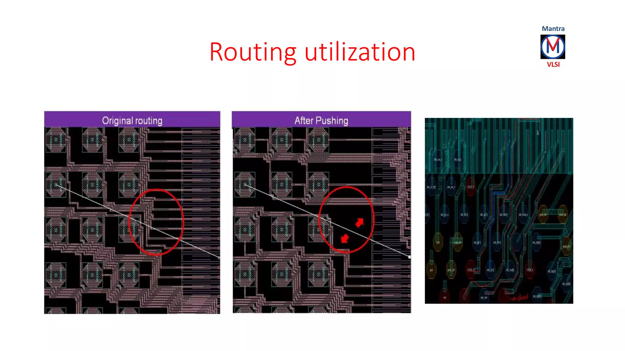
General aspects of routing efficiency in flip-chip designs.
Checklist criteria for verifying connectivity, length, width, resistance, area, noise, and power.
Acknowledgment and reference details regarding the content presented.
Introduction
This application notedescribes the die-driven flow with a peripheral ring I/O
style.
As silicon processes migrate to 45nm and below, flip-chip designs are becoming
more prevalent.
In the traditional design style, a designer places all I/Os around the core of a
design and bonding wires connect the die to the package.
In the flip-chip design style, there are no bonding wires.
The flip-chip design style makes it possible to increase the number of I/Os and
improve timing between I/O and core logic.
Flip-chip design requires a more sophisticated design methodology.
Packaging Technology
Integrated circuitsare put into protective packages to allow easy handling and
assembly onto printed circuit boards and to protect the devices from damage.
Some package types have standardized dimensions and tolerances, and are
registered with trade industry associations such as JEDEC and Pro Electron.
Other types are proprietary designations that
may be made by only one or two manufacturers.
Integrated circuit packaging is the last assembly
process before testing and shipping devices to
customers.
5.
Wirebonding
This conventional techniqueinvolves the mounting of a chip onto a substrate,
back-side down. Then, peripheral pads on the chip are bonded to the substrate
via wires.
The main advantage of this approach is that it is very cost-effective.
Machines have gotten to the point where tens of thousands of wires may be
bonded to chips and substrates within an hour.
6.
Drawbacks of Wirebonding
Thishigh throughput, along with a good record of reliability, have made
wirebonding the mainstream technique in chip-to-package interconnection.
However, there are many drawbacks to wirebonding which may prevent its
dominance in future designs. These include:
Peripheral nature of wirebonding makes it difficult to access internal parts of the
chip
Difficulty in shrinking pad pitches to < 50 mm
Thermal stability difficult to cool high-power chips
Susceptibility to simultaneous switching noise (high inductance of bonding wires)
7.
C4 Flip-Chip
C4 technologywas developed by IBM researchers in the 1960s.
The bonding process is characterized by the soldering of silicon devices directly
to a substrate (organic, for example).
The chip faces the substrate, as opposed to wirebonding, hence the name flip-
chip bonding. The salient features of this packaging methodology are as follows:
8.
C4 Flip-Chip
1) Solderbumps are distributed on metal terminals on the chip itself. These
solder bumps are typically composed of 97% lead and 3% Tin. The substrate has
identically placed metal pads on its surface.
2) The chip is turned over and the metal pads are aligned to solder bumps; metal
reflow is used to form connectivity between the substrate and chip.
9.
Advantages of C4technology
Increased I/O density C4 bumps may be placed over the entire area of the chip
(called area array) rather than simply the periphery.
Self-aligning process step due to surface tension
Reduced die size for previously pad limited designs
Reduced simultaneous switching noise due to smaller inductance of bumps
compared to wire leads
Better thermal properties as the backside of the wafer is now available for
heatsinking
Much better power distribution capabilities as circuits in the middle of the die
can now access Vdd/Gnd directly
Low cost and high throughput (all connections for one chip are made
simultaneously in C4 as opposed to one-by-one in wirebonding)
Shorter wirelengths and fewer global wires ease wiring requirements
10.
Drawbacks of C4technology
The main drawbacks to C4 at this time are that the use of lead in the solder
bumps lead to the emission of alpha particles which can lead to circuit failure in
sensitive circuits such as DRAM s.
However, this effect can be minimized by restricting the placement of solder
bumps over these sensitive areas.
Research is ongoing to find alternate materials for solber bumps as well.
Also, the use of C4 packaging allows designers to do many different things in the
floorplanning and routing stages of a design.
Commercial tools for place-and-route, etc. are predicated on the use of
peripheral wirebonding for I/O pads. New tools need to be in place for designers
to take full advantage of flip-chip s advantages.
11.
Flip Chip
Flip chipis the mounting of a chip with its active side facing the substrate.
This die orientation is “flipped” from the traditional packaging style, which uses
bonding wires to connect the package to the die.
In flip chip, the electrical interconnection between the chip and substrate is
established by using solder bumps.
Package-Driven or Bump-DrivenFlow
The IC package dictates the bump locations for the IC design.
All of the bump cells are instantiated and connected to flip-chip drivers as inputs
within the Verilog netlist.
The physical locations for the bump cells are predefined by the package designer.
Optimal flip-chip I/O driver locations are determined during flip-chip driver
placement based on the predefined bump locations.
14.
Die-Driven or IC-drivenFlow
The IC design dictates bump locations for the IC package.
Bump cells are not instantiated nor connected to flip-chip I/O drivers as inputs in
the Verilog netlist.
Optimal bump connections are determined after flip-chip driver and bump
pattern placement.
15.
Definition of Terms
PeripheralRing I/O
Flip-Chip Design Style The peripheral ring I/O flip-chip design style places flip-chip drivers outside the core
boundary, similar to the traditional peripheral I/O design style.
Bump cells can be placed on top of I/O drivers, or anywhere in the core.
CLASS PAD = I/O cell with bound pad.
Differentiating Area I/O
Area IO should be placed inside the core area
The LEF I/O Driver cells must contain CLASS PAD (for peripheral I/O) or CLASS PAD AREAIO (for area I/O).
CLASS PAD AREAIO = I/O cell without bump.
Flip-Chip Driver, I/O Driver, Driver
A flip-chip driver is an I/O circuit that connects to the bump to drive or receive signals.
The I/O driver cell includes a pad pin to connect to the flip-chip bump, and a signal pin to connect to the core
logic.
16.
Flip-Chip Bump, Flip-ChipPad, Bump Cell,
A bump structure consists of a solder ball placed on top of a large piece of metal
at the top metal layer.
The solder ball on the die connects to the solder ball on the package.
Standard cells can be placed under bump cells.
Bump cells can be placed over I/O drivers, if the I/O driver design supports this
application.
Signal bump cells connect to I/O driver cells and power bump cells connect to
power straps.
Bump Net
A bump net is a connection between a flip-chip I/O driver and a bump cell.
17.
Automatic Net Assignment
Assignmentis to logically connects flip-chip I/O drivers and bump cells in the die-
driven flow.
The flow requires automatic net assignment because there is no logical
connection between the driver and the bump in the Verilog netlist.
Automatic net assignment is not applicable for the package-driven flow, since the
package-driven flow connects bump cells to flip-chip I/O drivers within the
Verilog netlist.
Once logical connections are established, bump nets can be routed.
Redistribution Layer (RDL)
Routingredistributes the wire-bonding pads to the bump pads without changing
the placement of the I/O pads.
The redistribution layer is the top metal layer of the die.
Bump balls are placed on the redistribution layer and use the redistribution layer
to connect bump pads to wire-bonding pads.
Bump pitch &RDL spacing
1. Spacing: 86.630um available for RDL routing for 4 bumps
2. Max net length is ~800um(taken extra ~100), if we take 35X775 (W/L) RDL routing then resistance= 0.5 Ohm
3. Total space occupied by all the 3 bumps, 2 + 35 + 2 + 20 +2 + 20 +2 = 83 # if 3 rows bumps are P/G
1. If one signal comes in the second row then we can get 10um #only 2 rows with P/G and 3rd signal
2. The 1st row from the die should be routed direct within the boundary of the bump
Verilog Netlist Preparation
Asa minimum requirement, the input Verilog netlist must include core logic and
flip-chip I/O drivers instantiated and connected to the core logic.
Physical-only cells, such as ESD cells, can be added to the design in the IC
Compiler design flow and do not need to be in the Verilog netlist.
The die-driven flow does not require signal bump cells in the Verilog netlist.
Bump cells can be generated during bump pattern placement.
29.
Floorplan Creation
To createthe top-level floorplan, read the Verilog netlist using defined reference
and technology libraries.
Initialize the floorplan boundary, core height and width, utilization and core
offset.
You can also use the read_def command
to read a DEF file that contains placement
information.