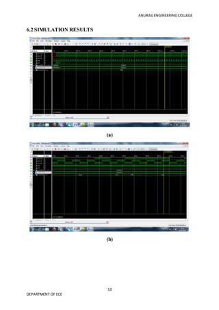
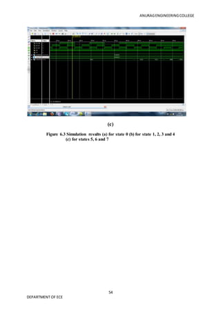
This document discusses the I2C bus protocol and its implementation on an FPGA to interface with low speed peripheral devices. It also provides background on VLSI design, including the evolution of integration density over time, the VLSI design flow from behavioral to layout representations, and historical context on increasing processing power needs driving advances in integration technologies. The I2C protocol allows communication between multiple chips using only two pins, addressing the need for lower pin counts as chip sizes decrease. The document implements I2C on an FPGA to interface with a DS1307 peripheral and synthesizes it on a Spartan 3E chip.
![ANURAGENGINEERINGCOLLEGE
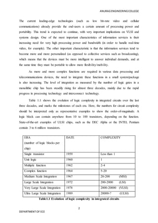
9
DEPARTMENT OF ECE
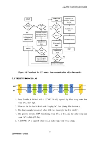
3. I
2
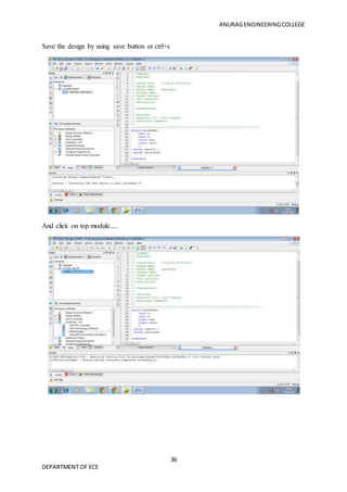
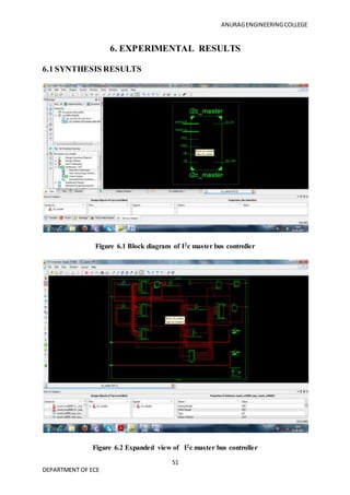
C Master Bus Controller
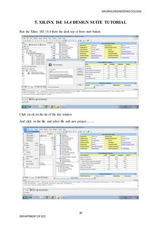
3.1 PROPOSED WORK
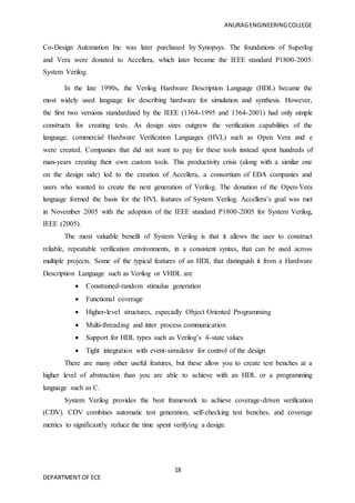
I2C is a two wire, bidirectional serial bus that provides effective data communication between
two devices. I2C bus supports many devices and each device is recognized by its unique
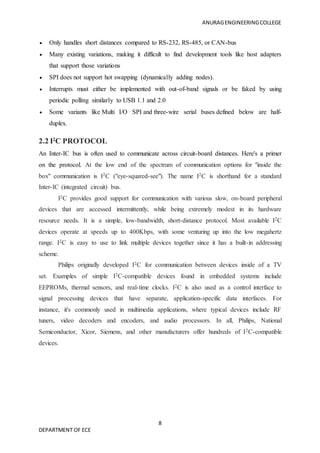
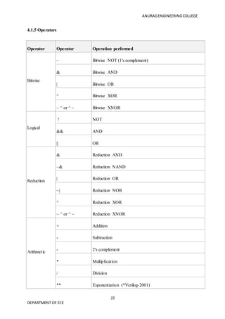
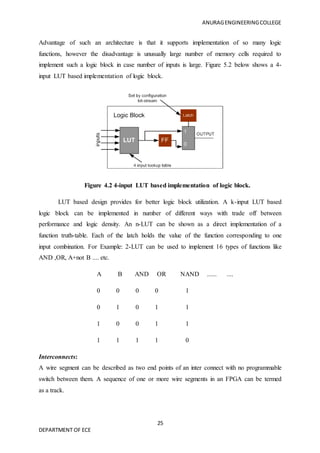
address. In Figure 3.1 data_in and addr_in are the 8 bit address given as an input. Clk and
reset are the input lines used to initiate the bus controller process. The R/ w signal is given
as an input to indicate whether master or slave acts as a transmitter in the data transmission.
data_in[7:0]
addr_in[6:0] SDA
Clk SCL
Reset
R/W‾‾
Figure 3.1 I2C Master Bus controller interfaced with slave DS1307
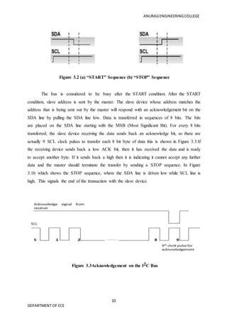
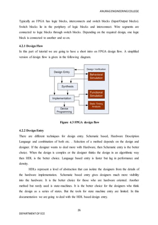
The physical I2C bus consists of just two wires, called SCL and SDA. SCL is the
clock line. It is used to synchronize all data transfers over the I2C bus. SDA is the data line.
The SCL and SDA lines are connected to all devices on the I2C bus. As both SCL and SDA
lines are "open drain" drivers they are pulled up using pull up resistors.The I2C bus is said to
be idle when both SCL and SDA are at logic 1 level. When the master (controller) wishes to
transmit data to a slave (DS1307) it begins by issuing a start sequence on the I2C bus,
which is a high to low transition on the SDA line while the SCL line is high as shown in
Figure 3.2.
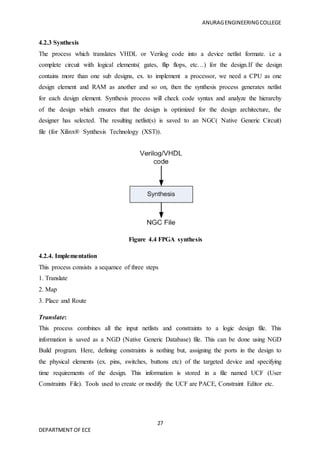
I2C
Master
Bus
Controller
DS1307
RTC](https://image.slidesharecdn.com/2a9c312e-5728-4ad1-a5db-b4791aa3146d-151115153345-lva1-app6891/85/MAJOR-PROJEC-TVLSI-9-320.jpg)
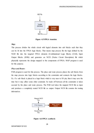
![ANURAGENGINEERINGCOLLEGE
56
DEPARTMENT OF ECE
REFERENCES
[1] Philips Semiconductor “I2C Bus Specification”version 2. 1, January 2000.
[2] Maxim integrated “DS1307 64 x 8, Serial, I2C Real Time Clock”, 2008.
[3] Prof. Jai Karan Singh “Design and Implementation of I2c master controller on
FPGA using VHDL,” IJET, Vol 4 No 4 Aug-Sep 2012.
[4] Raj kamal ,“Embedded system: Architecture programming and Design”,
Tata McGraw Hill,2008.
[5] Stuart Sutherland, “Verilog® HDL Quick Reference Guide”, IEEE Std 1364-
2001.
[6] Tim Wilmshurst, “Designing Embedded Systems with PIC Microcontrollers:
Principles and Applications” Elsevier Ltd publications, 2007.
[7] Xilinx “Spartan-3A/3AN FPGA Starter Kit Board User Guide,”version
1.1,2008.
[8] A.P.Godse,D.A.Godse,“Microprocessor, Microcontroller & Applications ”
Technical publications,2008.
[9] Vincent Himpe, “Mastering the I2C bus” Elektor Verlag publications, 2011.
[10] Pong P.Chu, “FPGA Prototyping By Verilog Examples:Xilinx Spartan–3
Version” Wiley,2008.
[11] Mano,Ciletti, “Digital Design”Pearson Education India,edition 4,2008.
[12] M.Morris Mano, “Digital Design” EBSCO publishing.Inc., 2002.
[13] Frank Vahid, “Digital Design with RTL Design, Verilog and VHDL”VP and
Executive](https://image.slidesharecdn.com/2a9c312e-5728-4ad1-a5db-b4791aa3146d-151115153345-lva1-app6891/85/MAJOR-PROJEC-TVLSI-56-320.jpg)


