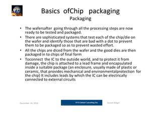
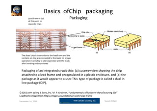
Download to read offline
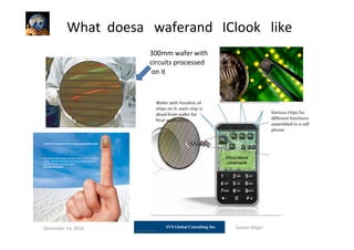
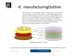
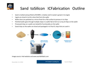

The document provides an overview of integrated circuit (IC) manufacturing. It discusses what an IC is, provides a brief history, and outlines the key steps in the manufacturing process. The process begins with purifying silicon ingots, slicing them into wafers, and polishing the wafers. The wafers then undergo multiple lithography, etching, and deposition steps to build transistors and interconnects. After processing, the dies on each wafer are tested and good dies are diced and packaged. The document explains some of the basic wafer processing steps like oxidation, resist coating, lithography, and etching in more detail. It aims to provide fundamentals of IC manufacturing.


![[Ultracode Munich Meetup #9] From Sand to Silicon by Christian Anderka](https://cdn.slidesharecdn.com/ss_thumbnails/sandtosiliconjuly-2015-150717130947-lva1-app6892-thumbnail.jpg?width=640&height=640&fit=bounds)


