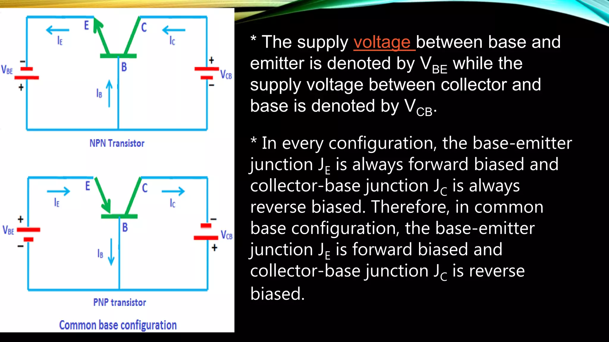
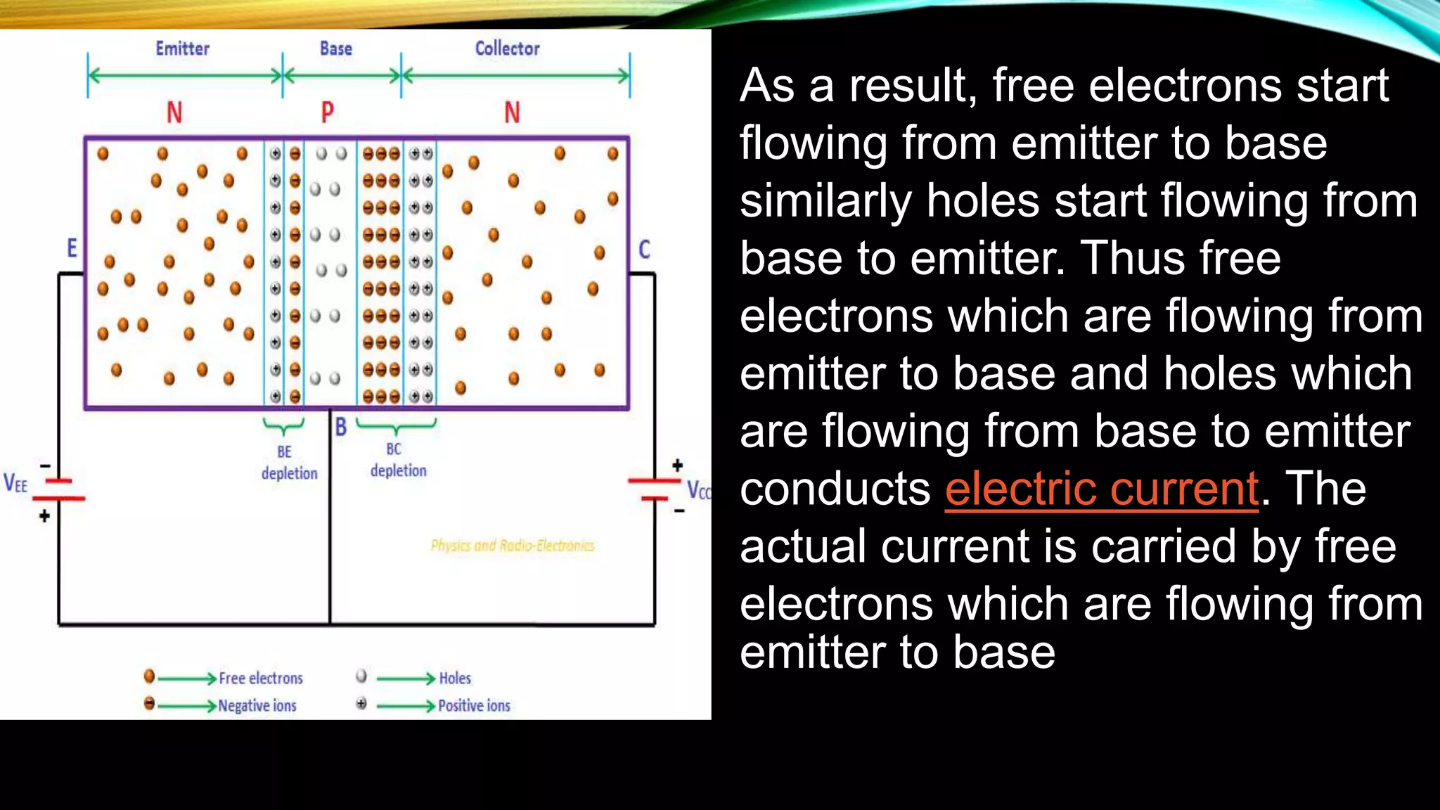
In common base configuration:
- The base terminal is common to both the input (emitter and base terminals) and output (collector and base terminals) of the transistor.
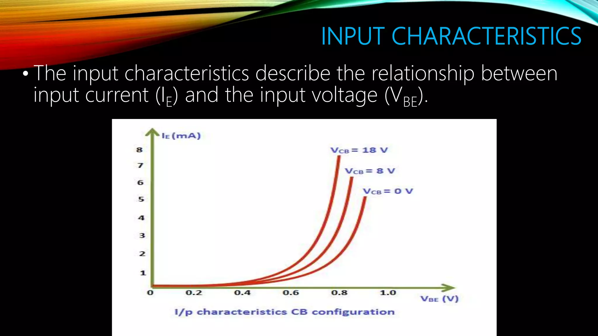
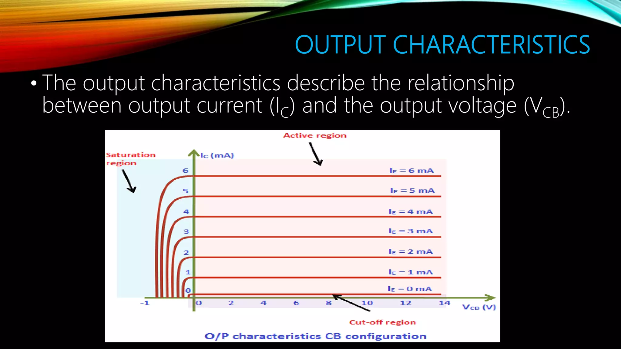
- The input signal is applied between the emitter and base terminals, while the output signal is taken from the collector and base terminals.
- The base-emitter junction is forward biased, allowing current to flow from the emitter to the base, while the collector-base junction is reverse biased.