Downloaded 45 times

![/amradelm
Introduction - PPA
• Digital VLSI chip design has mainly 3 targets
o Performance (timing)
o Power reduction
o Area reduction
• Failing to meet the area or power requirements will lead to higher fabrication cost, higher packing cost, short battery life, etc .
However, the chip will still operate correctly
• Failing to meet the timing/performance requirements will lead to a chip that doesn’t work and will require redesign to fix[1]
• Because of this, timing analysis remains the main and first priority of all design checks
2
[1] The fix can be simple like reducing the clock frequency or complex like changing the architecture](https://image.slidesharecdn.com/stapart1-240624003913-ffb50374/85/VLSI-Static-Timing-Analysis-Intro-Part-1-2-320.jpg)
![/amradelm
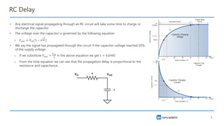
RC Delay – Cell Delay
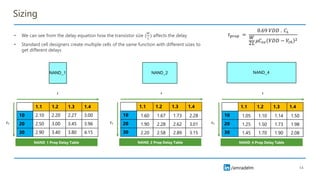
• To calculate the propagation delay of a logic gate we can approximate1 it as a simple RC
circuit. We will consider a simple inverter.
• When the input 𝑽𝒊𝒏 = 𝟎 :
o The upper PMOS is ON and the lower NMOS is OFF. Current will flow from the supply to
charge the 𝐶𝐿 capacitor from low to high.
o 𝑅𝑝𝑚𝑜𝑠 =
Δ𝑉
𝐼𝑝𝑚𝑜𝑠
=
𝑉𝐷𝐷
𝑊𝑝
2𝐿
𝜇𝑝𝐶𝑜𝑥 𝑉𝐷𝐷−𝑉𝑡ℎ
2
o 𝑡𝐿𝐻 = 0.69𝑅𝑝𝑚𝑜𝑠𝐶𝐿 =
0.69 𝑉𝐷𝐷 . 𝐶𝐿
𝑊𝑝
2𝐿
𝜇𝑝𝐶𝑜𝑥 𝑉𝐷𝐷−𝑉𝑡ℎ
2
• When the input 𝑽𝒊𝒏 = 𝑽𝑫𝑫 :
o The upper PMOS is OFF and the lower NMOS is ON. Current will flow from the capacitor
to ground to discharge the 𝐶𝐿 capacitor from high to low.
o 𝑅𝑛𝑚𝑜𝑠 =
Δ𝑉
𝐼𝑛𝑚𝑜𝑠
=
𝑉𝐷𝐷
𝑊𝑛
2𝐿
𝜇𝑛𝐶𝑜𝑥 𝑉𝐷𝐷−𝑉𝑡ℎ
2
o 𝑡𝐻𝐿 = 0.69𝑅𝑛𝑚𝑜𝑠𝐶𝐿 =
0.69 𝑉𝐷𝐷 . 𝐶𝐿
𝑊𝑛
2𝐿
𝜇𝑛𝐶𝑜𝑥 𝑉𝐷𝐷−𝑉𝑡ℎ
2
6
[1] For an accurate calculations : https://classes.engineering.wustl.edu/cse463/Chapter_6_CSE463.pdf](https://image.slidesharecdn.com/stapart1-240624003913-ffb50374/85/VLSI-Static-Timing-Analysis-Intro-Part-1-6-320.jpg)

![/amradelm
References
• [1] https://classes.engineering.wustl.edu/cse463/Chapter_6_CSE463.pdf
• [2] https://www.iue.tuwien.ac.at/phd/park/node30.html
• [3] https://www.electronics-tutorials.ws/rc/rc_1.html
• [4] http://web.mit.edu/6.012/www/SP07-L13.pdf
• [5] https://www.linkedin.com/pulse/understanding-power-performance-area-ppa-analysis-vlsi-priya-pandey/
• [6] https://citeseerx.ist.psu.edu/document?repid=rep1&type=pdf&doi=ecc04789069f3e19bebe5814ce3608aa609e4403
25](https://image.slidesharecdn.com/stapart1-240624003913-ffb50374/85/VLSI-Static-Timing-Analysis-Intro-Part-1-25-320.jpg)


The document provides an overview of static timing analysis in digital VLSI chip design, highlighting that timing is the primary focus to ensure functionality post-fabrication. It details key timing checks necessary for validation, such as setup and hold timing, and discusses the propagation delay in RC circuits, emphasizing the factors influencing delay, including resistance, capacitance, and transistor sizing. The document also explains how designers use timing tables and calculations to determine timing paths and optimize chip performance.


![[Back2School] Delay Calculation- Chapter 2](https://cdn.slidesharecdn.com/ss_thumbnails/delaycalculation-250530192911-03116e20-thumbnail.jpg?width=640&height=640&fit=bounds)