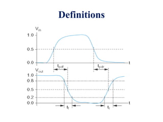
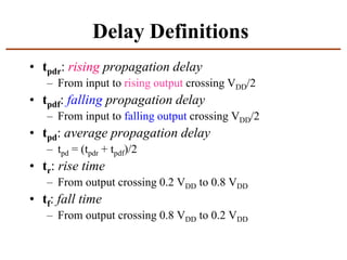
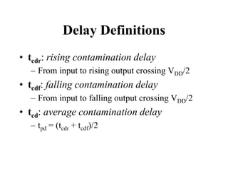
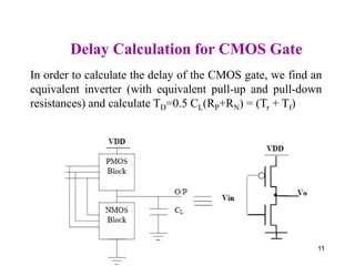
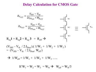
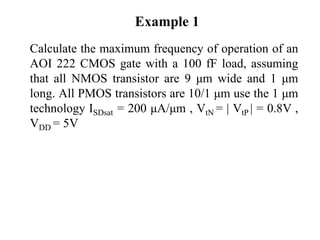
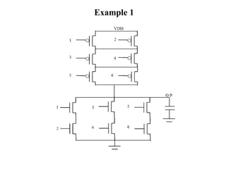
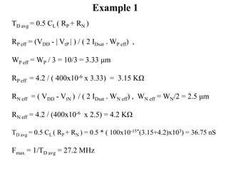
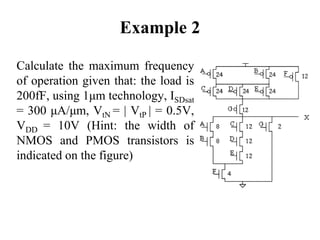
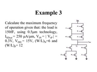
SlideShare a Scribd company logo
1 of 19
CMOS Delay
Dr. Ahmed Youssef
COE 360
Principles of VLSI
Design
Definitions
Delay Definitions
• tpdr: rising propagation delay
– From input to rising output crossing VDD/2
• tpdf: falling propagation delay
– From input to falling output crossing VDD/2
• tpd: average propagation delay
– tpd = (tpdr + tpdf)/2
• tr: rise time
– From output crossing 0.2 VDD to 0.8 VDD
• tf: fall time
– From output crossing 0.8 VDD to 0.2 VDD
Delay Definitions
• tcdr: rising contamination delay
– From input to rising output crossing VDD/2
• tcdf: falling contamination delay
– From input to falling output crossing VDD/2
• tcd: average contamination delay
– tpd = (tcdr + tcdf)/2
Definitions
Propagation Delay – Time from last input
change until last output change.
Contamination Delay – Time from first input
change until first output change.
Best-case (contamination) delay can be substantially
less than propagation delay.
Definitions
• A timing analyzer computes the arrival times, i.e.,
the latest time at which each node in a block of
logic will switch.
• The nodes are classified as inputs, outputs, and
internal nodes.
Definitions
• The arrival time ai at internal node i depends on
the propagation delay of the gate driving i and the
arrival times of the inputs to the gate:
Definitions
• The slack is the difference between the required and
arrival times.
• Positive slack means that the circuit meets timing.
• Negative slack means that the circuit is not fast enough.
Example
• Nodes annotated with arrival times. If the outputs
are all required at 200 ps, the circuit has 60 ps of
slack.
9
Delay Estimation
11
11
11
Delay Calculation for CMOS Gate
In order to calculate the delay of the CMOS gate, we find an
equivalent inverter (with equivalent pull-up and pull-down
resistances) and calculate TD=0.5 CL(RP+RN) = (Tr + Tf)
Delay Calculation for CMOS Gate
Where Tr and Tf of the equivalent
inverter = worst case Tr and Tf of the
gate
Worst case Tr occur when the O/P is
charged (or pulled-up) through the
longest chain of series PMOS
transistors: e.g. for the PU block
below
Worst case charging is when B = D
= H = 1 And A = C = E = 0 i.e.
charging through A,C, & E
Delay Calculation for CMOS Gate
Similarly, worst case Tf occurs when discharging the output
through the longest discharging path
For the PD block below, Worst case : 1,4,6 are ON or 2,4,6 or
3,4,6 while every other transistor is off
Delay Calculation for CMOS Gate
𝑅𝑃𝑒𝑓𝑓
=
𝑉𝐷𝐷 − 𝑉𝑡𝑝
2𝐼𝑆𝐷𝑠𝑎𝑡
∗ 𝑊
𝑝𝑒𝑓𝑓
𝑅𝑁𝑒𝑓𝑓
=
𝑉𝐷𝐷 − 𝑉𝑡𝑛
2𝐼𝐷𝑆𝑠𝑎𝑡
∗ 𝑊
𝑛𝑒𝑓𝑓
Req1 + Req2 + Req 3 = Reff 
(VDD – Vth / 2.IDsat ).( 1/W1 + 1/W2 + 1/W3 )
= (VDD – Vth / 2.IDsat. Weff )
 1/Weff = 1/W1 + 1/W2 + 1/W3 …..
W1
W2
W3
Weff
If W1 = W2 = W3 = WN  Weff = WN/3
Example 1
Calculate the maximum frequency of operation of an
AOI 222 CMOS gate with a 100 fF load, assuming
that all NMOS transistor are 9 μm wide and 1 μm
long. All PMOS transistors are 10/1 μm use the 1 μm
technology ISDsat = 200 μA/μm , VtN = | VtP | = 0.8V ,
VDD = 5V
Example 1
TD avg = 0.5 CL ( RP + RN )
RP eff = (VDD - | VtP | ) / ( 2 IDsat . WP eff) ,
WP eff = WP / 3 = 10/3 = 3.33 μm
RP eff = 4.2 / ( 400x10-6 x 3.33) = 3.15 KΩ
RN eff = ( VDD - VtN ) / ( 2 IDsat . WN eff) , WN eff = WN/2 = 2.5 μm
RN eff = 4.2 / (400x10-6 x 2.5) = 4.2 KΩ
TD avg = 0.5 CL ( RP + RN ) = 0.5 * ( 100x10-15*(3.15+4.2)x103) = 36.75 nS
Fmax = 1/TD avg = 27.2 MHz
Example 1
Example 2
Calculate the maximum frequency
of operation given that: the load is
200fF, using 1μm technology, ISDsat
= 300 μA/μm, VtN = | VtP | = 0.5V,
VDD = 10V (Hint: the width of
NMOS and PMOS transistors is
indicated on the figure)
Example 3
Calculate the maximum frequency
of operation given that: the load is
150fF, using 0.5μm technology,
ISDsat = 250 μA/μm, VtN = | VtP | =
0.3V, VDD = 15V, (W/L)N=6 and
(W/L)P= 12

More Related Content

Similar to 4-CMOS-Delay.pptx

Original Mosfet N FDPF8N50NZ 8N50 8N50NZ 10V 4A TO-220 New Fairchild
Original Mosfet N FDPF8N50NZ 8N50 8N50NZ 10V 4A TO-220 New FairchildOriginal Mosfet N FDPF8N50NZ 8N50 8N50NZ 10V 4A TO-220 New Fairchild
Original Mosfet N FDPF8N50NZ 8N50 8N50NZ 10V 4A TO-220 New FairchildAUTHELECTRONIC
 
FQP50N06L.pdf
FQP50N06L.pdfFQP50N06L.pdf
FQP50N06L.pdfivan ion
 
Original MOSFET N-CHANNEL FQPF9N50C 9N50C 9N50 TO-220 9A 500V New
Original MOSFET N-CHANNEL FQPF9N50C 9N50C 9N50 TO-220 9A 500V NewOriginal MOSFET N-CHANNEL FQPF9N50C 9N50C 9N50 TO-220 9A 500V New
Original MOSFET N-CHANNEL FQPF9N50C 9N50C 9N50 TO-220 9A 500V NewAUTHELECTRONIC
 
Advd lecture 08 -inverte rpart3
Advd   lecture 08 -inverte rpart3Advd   lecture 08 -inverte rpart3
Advd lecture 08 -inverte rpart3Hardik Gupta
 
Original MOSFET N-CHANNEL FQPF13N50C FQPF13N50 13N50 TO-220 13A 500V New
Original MOSFET N-CHANNEL FQPF13N50C FQPF13N50 13N50 TO-220 13A 500V NewOriginal MOSFET N-CHANNEL FQPF13N50C FQPF13N50 13N50 TO-220 13A 500V New
Original MOSFET N-CHANNEL FQPF13N50C FQPF13N50 13N50 TO-220 13A 500V NewAUTHELECTRONIC
 
1999 si pi_dws_training_course
1999 si pi_dws_training_course1999 si pi_dws_training_course
1999 si pi_dws_training_coursePiero Belforte
 
synthetic aperture radar
synthetic aperture radarsynthetic aperture radar
synthetic aperture radarAmit Rastogi
 
Original N-Channel Mosfet IRFI4019H-117P 4019 8A 150V TO-220 New
Original N-Channel Mosfet IRFI4019H-117P 4019 8A 150V TO-220 NewOriginal N-Channel Mosfet IRFI4019H-117P 4019 8A 150V TO-220 New
Original N-Channel Mosfet IRFI4019H-117P 4019 8A 150V TO-220 NewAUTHELECTRONIC
 
Original N-Channel Mosfet IRFI4019H-117P 4019 8A 150V TO-220 New
Original N-Channel Mosfet IRFI4019H-117P 4019 8A 150V TO-220 NewOriginal N-Channel Mosfet IRFI4019H-117P 4019 8A 150V TO-220 New
Original N-Channel Mosfet IRFI4019H-117P 4019 8A 150V TO-220 NewAUTHELECTRONIC
 
Transformer overcurrent
Transformer overcurrentTransformer overcurrent
Transformer overcurrentmichaeljmack
 
Si Intro(100413)
Si Intro(100413)Si Intro(100413)
Si Intro(100413)imsong
 
Original Mosfet 4N90C FQP4N90C FQP4N90 900V 4A TO-220 New
Original Mosfet 4N90C FQP4N90C FQP4N90 900V 4A TO-220 NewOriginal Mosfet 4N90C FQP4N90C FQP4N90 900V 4A TO-220 New
Original Mosfet 4N90C FQP4N90C FQP4N90 900V 4A TO-220 NewAUTHELECTRONIC
 
Original N-Channel Mosfet 20N06 FQP20N06 60V 20A TO-220 New Fairchild
Original N-Channel Mosfet 20N06 FQP20N06 60V 20A TO-220 New FairchildOriginal N-Channel Mosfet 20N06 FQP20N06 60V 20A TO-220 New Fairchild
Original N-Channel Mosfet 20N06 FQP20N06 60V 20A TO-220 New FairchildAUTHELECTRONIC
 
FDP047AN08A0.pdf
FDP047AN08A0.pdfFDP047AN08A0.pdf
FDP047AN08A0.pdfivan ion
 
03 6420 e-utra layer 1 key aspects and ofdm(a) principles_e05
03 6420 e-utra layer 1 key aspects and ofdm(a) principles_e0503 6420 e-utra layer 1 key aspects and ofdm(a) principles_e05
03 6420 e-utra layer 1 key aspects and ofdm(a) principles_e05ElhamTagharobi
 
Original N-Channel Mosfet FQP3N80C 3N80C 3A 800V TO-220F New FAIRCHILD
Original N-Channel Mosfet FQP3N80C 3N80C 3A 800V TO-220F New FAIRCHILDOriginal N-Channel Mosfet FQP3N80C 3N80C 3A 800V TO-220F New FAIRCHILD
Original N-Channel Mosfet FQP3N80C 3N80C 3A 800V TO-220F New FAIRCHILDAUTHELECTRONIC
 

Similar to 4-CMOS-Delay.pptx (20)

Original Mosfet N FDPF8N50NZ 8N50 8N50NZ 10V 4A TO-220 New Fairchild
Original Mosfet N FDPF8N50NZ 8N50 8N50NZ 10V 4A TO-220 New FairchildOriginal Mosfet N FDPF8N50NZ 8N50 8N50NZ 10V 4A TO-220 New Fairchild
Original Mosfet N FDPF8N50NZ 8N50 8N50NZ 10V 4A TO-220 New Fairchild
 
FQP50N06L.pdf
FQP50N06L.pdfFQP50N06L.pdf
FQP50N06L.pdf
 
Original MOSFET N-CHANNEL FQPF9N50C 9N50C 9N50 TO-220 9A 500V New
Original MOSFET N-CHANNEL FQPF9N50C 9N50C 9N50 TO-220 9A 500V NewOriginal MOSFET N-CHANNEL FQPF9N50C 9N50C 9N50 TO-220 9A 500V New
Original MOSFET N-CHANNEL FQPF9N50C 9N50C 9N50 TO-220 9A 500V New
 
Advd lecture 08 -inverte rpart3
Advd   lecture 08 -inverte rpart3Advd   lecture 08 -inverte rpart3
Advd lecture 08 -inverte rpart3
 
ofdm
ofdmofdm
ofdm
 
Original MOSFET N-CHANNEL FQPF13N50C FQPF13N50 13N50 TO-220 13A 500V New
Original MOSFET N-CHANNEL FQPF13N50C FQPF13N50 13N50 TO-220 13A 500V NewOriginal MOSFET N-CHANNEL FQPF13N50C FQPF13N50 13N50 TO-220 13A 500V New
Original MOSFET N-CHANNEL FQPF13N50C FQPF13N50 13N50 TO-220 13A 500V New
 
Chap2 ofdm basics
Chap2 ofdm basicsChap2 ofdm basics
Chap2 ofdm basics
 
Analog Communication Lab Manual
Analog Communication Lab ManualAnalog Communication Lab Manual
Analog Communication Lab Manual
 
1999 si pi_dws_training_course
1999 si pi_dws_training_course1999 si pi_dws_training_course
1999 si pi_dws_training_course
 
07_Digital timing_&_Pipelining.ppt
07_Digital timing_&_Pipelining.ppt07_Digital timing_&_Pipelining.ppt
07_Digital timing_&_Pipelining.ppt
 
synthetic aperture radar
synthetic aperture radarsynthetic aperture radar
synthetic aperture radar
 
Original N-Channel Mosfet IRFI4019H-117P 4019 8A 150V TO-220 New
Original N-Channel Mosfet IRFI4019H-117P 4019 8A 150V TO-220 NewOriginal N-Channel Mosfet IRFI4019H-117P 4019 8A 150V TO-220 New
Original N-Channel Mosfet IRFI4019H-117P 4019 8A 150V TO-220 New
 
Original N-Channel Mosfet IRFI4019H-117P 4019 8A 150V TO-220 New
Original N-Channel Mosfet IRFI4019H-117P 4019 8A 150V TO-220 NewOriginal N-Channel Mosfet IRFI4019H-117P 4019 8A 150V TO-220 New
Original N-Channel Mosfet IRFI4019H-117P 4019 8A 150V TO-220 New
 
Transformer overcurrent
Transformer overcurrentTransformer overcurrent
Transformer overcurrent
 
Si Intro(100413)
Si Intro(100413)Si Intro(100413)
Si Intro(100413)
 
Original Mosfet 4N90C FQP4N90C FQP4N90 900V 4A TO-220 New
Original Mosfet 4N90C FQP4N90C FQP4N90 900V 4A TO-220 NewOriginal Mosfet 4N90C FQP4N90C FQP4N90 900V 4A TO-220 New
Original Mosfet 4N90C FQP4N90C FQP4N90 900V 4A TO-220 New
 
Original N-Channel Mosfet 20N06 FQP20N06 60V 20A TO-220 New Fairchild
Original N-Channel Mosfet 20N06 FQP20N06 60V 20A TO-220 New FairchildOriginal N-Channel Mosfet 20N06 FQP20N06 60V 20A TO-220 New Fairchild
Original N-Channel Mosfet 20N06 FQP20N06 60V 20A TO-220 New Fairchild
 
FDP047AN08A0.pdf
FDP047AN08A0.pdfFDP047AN08A0.pdf
FDP047AN08A0.pdf
 
03 6420 e-utra layer 1 key aspects and ofdm(a) principles_e05
03 6420 e-utra layer 1 key aspects and ofdm(a) principles_e0503 6420 e-utra layer 1 key aspects and ofdm(a) principles_e05
03 6420 e-utra layer 1 key aspects and ofdm(a) principles_e05
 
Original N-Channel Mosfet FQP3N80C 3N80C 3A 800V TO-220F New FAIRCHILD
Original N-Channel Mosfet FQP3N80C 3N80C 3A 800V TO-220F New FAIRCHILDOriginal N-Channel Mosfet FQP3N80C 3N80C 3A 800V TO-220F New FAIRCHILD
Original N-Channel Mosfet FQP3N80C 3N80C 3A 800V TO-220F New FAIRCHILD
 

Recently uploaded

怎样办理圣芭芭拉分校毕业证(UCSB毕业证书)成绩单留信认证
怎样办理圣芭芭拉分校毕业证(UCSB毕业证书)成绩单留信认证怎样办理圣芭芭拉分校毕业证(UCSB毕业证书)成绩单留信认证
怎样办理圣芭芭拉分校毕业证(UCSB毕业证书)成绩单留信认证ehyxf
 
🌹Patia⬅️ Vip Call Girls Bhubaneswar 📱9777949614 Book Well Trand Call Girls In...
🌹Patia⬅️ Vip Call Girls Bhubaneswar 📱9777949614 Book Well Trand Call Girls In...🌹Patia⬅️ Vip Call Girls Bhubaneswar 📱9777949614 Book Well Trand Call Girls In...
🌹Patia⬅️ Vip Call Girls Bhubaneswar 📱9777949614 Book Well Trand Call Girls In...Call Girls Mumbai
 
在线制作(ANU毕业证书)澳大利亚国立大学毕业证成绩单原版一比一
在线制作(ANU毕业证书)澳大利亚国立大学毕业证成绩单原版一比一在线制作(ANU毕业证书)澳大利亚国立大学毕业证成绩单原版一比一
在线制作(ANU毕业证书)澳大利亚国立大学毕业证成绩单原版一比一ougvy
 
Vashi Affordable Call Girls ,07506202331,Vasai Virar Charming Call Girl
Vashi Affordable Call Girls ,07506202331,Vasai Virar Charming Call GirlVashi Affordable Call Girls ,07506202331,Vasai Virar Charming Call Girl
Vashi Affordable Call Girls ,07506202331,Vasai Virar Charming Call GirlPriya Reddy
 
Top profile Call Girls In Palghar [ 7014168258 ] Call Me For Genuine Models W...
Top profile Call Girls In Palghar [ 7014168258 ] Call Me For Genuine Models W...Top profile Call Girls In Palghar [ 7014168258 ] Call Me For Genuine Models W...
Top profile Call Girls In Palghar [ 7014168258 ] Call Me For Genuine Models W...gajnagarg
 
在线办理(scu毕业证)南十字星大学毕业证电子版学位证书注册证明信
在线办理(scu毕业证)南十字星大学毕业证电子版学位证书注册证明信在线办理(scu毕业证)南十字星大学毕业证电子版学位证书注册证明信
在线办理(scu毕业证)南十字星大学毕业证电子版学位证书注册证明信oopacde
 
一比一原版(RMIT毕业证书)墨尔本皇家理工大学毕业证成绩单学位证靠谱定制
一比一原版(RMIT毕业证书)墨尔本皇家理工大学毕业证成绩单学位证靠谱定制一比一原版(RMIT毕业证书)墨尔本皇家理工大学毕业证成绩单学位证靠谱定制
一比一原版(RMIT毕业证书)墨尔本皇家理工大学毕业证成绩单学位证靠谱定制ougvy
 
一比一原版(Otago毕业证书)奥塔哥理工学院毕业证成绩单学位证靠谱定制
一比一原版(Otago毕业证书)奥塔哥理工学院毕业证成绩单学位证靠谱定制一比一原版(Otago毕业证书)奥塔哥理工学院毕业证成绩单学位证靠谱定制
一比一原版(Otago毕业证书)奥塔哥理工学院毕业证成绩单学位证靠谱定制uodye
 
Call Girls in Bhubaneswar Patia Escort Service(🔝))/WhatsApp 97779⇛49614
Call Girls in Bhubaneswar Patia Escort Service(🔝))/WhatsApp 97779⇛49614Call Girls in Bhubaneswar Patia Escort Service(🔝))/WhatsApp 97779⇛49614
Call Girls in Bhubaneswar Patia Escort Service(🔝))/WhatsApp 97779⇛49614jabtakhaidam7
 
一比一定(购)坎特伯雷大学毕业证(UC毕业证)成绩单学位证
一比一定(购)坎特伯雷大学毕业证(UC毕业证)成绩单学位证一比一定(购)坎特伯雷大学毕业证(UC毕业证)成绩单学位证
一比一定(购)坎特伯雷大学毕业证(UC毕业证)成绩单学位证wpkuukw
 
£ HAMIL 5 BULAN £ CARA MENGGUGURKAN KANDUNGAN USIA 5 BULAN ((087776558899))
£ HAMIL 5 BULAN £ CARA MENGGUGURKAN KANDUNGAN USIA 5 BULAN ((087776558899))£ HAMIL 5 BULAN £ CARA MENGGUGURKAN KANDUNGAN USIA 5 BULAN ((087776558899))
£ HAMIL 5 BULAN £ CARA MENGGUGURKAN KANDUNGAN USIA 5 BULAN ((087776558899))Obat Cytotec
 
Call Girls Service Lucknow {0000000000 } ❤️VVIP BHAWNA Call Girl in Lucknow U.P
Call Girls Service Lucknow {0000000000 } ❤️VVIP BHAWNA Call Girl in Lucknow U.PCall Girls Service Lucknow {0000000000 } ❤️VVIP BHAWNA Call Girl in Lucknow U.P
Call Girls Service Lucknow {0000000000 } ❤️VVIP BHAWNA Call Girl in Lucknow U.Pjabtakhaidam7
 
NON INVASIVE GLUCOSE BLODD MONITORING SYSTEM (1) (2) (1).pptx
NON INVASIVE GLUCOSE BLODD MONITORING SYSTEM (1) (2) (1).pptxNON INVASIVE GLUCOSE BLODD MONITORING SYSTEM (1) (2) (1).pptx
NON INVASIVE GLUCOSE BLODD MONITORING SYSTEM (1) (2) (1).pptxSimmySharma12
 
Nava Vadaj * Call Girl in Ahmedabad - Phone 8005736733 Escorts Service at 6k ...
Nava Vadaj * Call Girl in Ahmedabad - Phone 8005736733 Escorts Service at 6k ...Nava Vadaj * Call Girl in Ahmedabad - Phone 8005736733 Escorts Service at 6k ...
Nava Vadaj * Call Girl in Ahmedabad - Phone 8005736733 Escorts Service at 6k ...gragfaguni
 
一比一原版(CSUEB毕业证书)东湾分校毕业证原件一模一样
一比一原版(CSUEB毕业证书)东湾分校毕业证原件一模一样一比一原版(CSUEB毕业证书)东湾分校毕业证原件一模一样
一比一原版(CSUEB毕业证书)东湾分校毕业证原件一模一样ayoqf
 
Call Girls Amethi 9332606886 HOT & SEXY Models beautiful and charming call g...
Call Girls Amethi  9332606886 HOT & SEXY Models beautiful and charming call g...Call Girls Amethi  9332606886 HOT & SEXY Models beautiful and charming call g...
Call Girls Amethi 9332606886 HOT & SEXY Models beautiful and charming call g...Sareena Khatun
 

Recently uploaded (20)

怎样办理圣芭芭拉分校毕业证(UCSB毕业证书)成绩单留信认证
怎样办理圣芭芭拉分校毕业证(UCSB毕业证书)成绩单留信认证怎样办理圣芭芭拉分校毕业证(UCSB毕业证书)成绩单留信认证
怎样办理圣芭芭拉分校毕业证(UCSB毕业证书)成绩单留信认证
 
Abortion Pills in Jeddah |+966572737505 | Get Cytotec
Abortion Pills in Jeddah |+966572737505 | Get CytotecAbortion Pills in Jeddah |+966572737505 | Get Cytotec
Abortion Pills in Jeddah |+966572737505 | Get Cytotec
 
Contact +971581248768 to buy 100% original and safe abortion pills in Dubai a...
Contact +971581248768 to buy 100% original and safe abortion pills in Dubai a...Contact +971581248768 to buy 100% original and safe abortion pills in Dubai a...
Contact +971581248768 to buy 100% original and safe abortion pills in Dubai a...
 
Abortion pills in Jeddah |+966572737505 | Get Cytotec
Abortion pills in Jeddah |+966572737505 | Get CytotecAbortion pills in Jeddah |+966572737505 | Get Cytotec
Abortion pills in Jeddah |+966572737505 | Get Cytotec
 
🌹Patia⬅️ Vip Call Girls Bhubaneswar 📱9777949614 Book Well Trand Call Girls In...
🌹Patia⬅️ Vip Call Girls Bhubaneswar 📱9777949614 Book Well Trand Call Girls In...🌹Patia⬅️ Vip Call Girls Bhubaneswar 📱9777949614 Book Well Trand Call Girls In...
🌹Patia⬅️ Vip Call Girls Bhubaneswar 📱9777949614 Book Well Trand Call Girls In...
 
在线制作(ANU毕业证书)澳大利亚国立大学毕业证成绩单原版一比一
在线制作(ANU毕业证书)澳大利亚国立大学毕业证成绩单原版一比一在线制作(ANU毕业证书)澳大利亚国立大学毕业证成绩单原版一比一
在线制作(ANU毕业证书)澳大利亚国立大学毕业证成绩单原版一比一
 
Vashi Affordable Call Girls ,07506202331,Vasai Virar Charming Call Girl
Vashi Affordable Call Girls ,07506202331,Vasai Virar Charming Call GirlVashi Affordable Call Girls ,07506202331,Vasai Virar Charming Call Girl
Vashi Affordable Call Girls ,07506202331,Vasai Virar Charming Call Girl
 
Buy Abortion pills in Riyadh |+966572737505 | Get Cytotec
Buy Abortion pills in Riyadh |+966572737505 | Get CytotecBuy Abortion pills in Riyadh |+966572737505 | Get Cytotec
Buy Abortion pills in Riyadh |+966572737505 | Get Cytotec
 
Top profile Call Girls In Palghar [ 7014168258 ] Call Me For Genuine Models W...
Top profile Call Girls In Palghar [ 7014168258 ] Call Me For Genuine Models W...Top profile Call Girls In Palghar [ 7014168258 ] Call Me For Genuine Models W...
Top profile Call Girls In Palghar [ 7014168258 ] Call Me For Genuine Models W...
 
在线办理(scu毕业证)南十字星大学毕业证电子版学位证书注册证明信
在线办理(scu毕业证)南十字星大学毕业证电子版学位证书注册证明信在线办理(scu毕业证)南十字星大学毕业证电子版学位证书注册证明信
在线办理(scu毕业证)南十字星大学毕业证电子版学位证书注册证明信
 
一比一原版(RMIT毕业证书)墨尔本皇家理工大学毕业证成绩单学位证靠谱定制
一比一原版(RMIT毕业证书)墨尔本皇家理工大学毕业证成绩单学位证靠谱定制一比一原版(RMIT毕业证书)墨尔本皇家理工大学毕业证成绩单学位证靠谱定制
一比一原版(RMIT毕业证书)墨尔本皇家理工大学毕业证成绩单学位证靠谱定制
 
一比一原版(Otago毕业证书)奥塔哥理工学院毕业证成绩单学位证靠谱定制
一比一原版(Otago毕业证书)奥塔哥理工学院毕业证成绩单学位证靠谱定制一比一原版(Otago毕业证书)奥塔哥理工学院毕业证成绩单学位证靠谱定制
一比一原版(Otago毕业证书)奥塔哥理工学院毕业证成绩单学位证靠谱定制
 
Call Girls in Bhubaneswar Patia Escort Service(🔝))/WhatsApp 97779⇛49614
Call Girls in Bhubaneswar Patia Escort Service(🔝))/WhatsApp 97779⇛49614Call Girls in Bhubaneswar Patia Escort Service(🔝))/WhatsApp 97779⇛49614
Call Girls in Bhubaneswar Patia Escort Service(🔝))/WhatsApp 97779⇛49614
 
一比一定(购)坎特伯雷大学毕业证(UC毕业证)成绩单学位证
一比一定(购)坎特伯雷大学毕业证(UC毕业证)成绩单学位证一比一定(购)坎特伯雷大学毕业证(UC毕业证)成绩单学位证
一比一定(购)坎特伯雷大学毕业证(UC毕业证)成绩单学位证
 
£ HAMIL 5 BULAN £ CARA MENGGUGURKAN KANDUNGAN USIA 5 BULAN ((087776558899))
£ HAMIL 5 BULAN £ CARA MENGGUGURKAN KANDUNGAN USIA 5 BULAN ((087776558899))£ HAMIL 5 BULAN £ CARA MENGGUGURKAN KANDUNGAN USIA 5 BULAN ((087776558899))
£ HAMIL 5 BULAN £ CARA MENGGUGURKAN KANDUNGAN USIA 5 BULAN ((087776558899))
 
Call Girls Service Lucknow {0000000000 } ❤️VVIP BHAWNA Call Girl in Lucknow U.P
Call Girls Service Lucknow {0000000000 } ❤️VVIP BHAWNA Call Girl in Lucknow U.PCall Girls Service Lucknow {0000000000 } ❤️VVIP BHAWNA Call Girl in Lucknow U.P
Call Girls Service Lucknow {0000000000 } ❤️VVIP BHAWNA Call Girl in Lucknow U.P
 
NON INVASIVE GLUCOSE BLODD MONITORING SYSTEM (1) (2) (1).pptx
NON INVASIVE GLUCOSE BLODD MONITORING SYSTEM (1) (2) (1).pptxNON INVASIVE GLUCOSE BLODD MONITORING SYSTEM (1) (2) (1).pptx
NON INVASIVE GLUCOSE BLODD MONITORING SYSTEM (1) (2) (1).pptx
 
Nava Vadaj * Call Girl in Ahmedabad - Phone 8005736733 Escorts Service at 6k ...
Nava Vadaj * Call Girl in Ahmedabad - Phone 8005736733 Escorts Service at 6k ...Nava Vadaj * Call Girl in Ahmedabad - Phone 8005736733 Escorts Service at 6k ...
Nava Vadaj * Call Girl in Ahmedabad - Phone 8005736733 Escorts Service at 6k ...
 
一比一原版(CSUEB毕业证书)东湾分校毕业证原件一模一样
一比一原版(CSUEB毕业证书)东湾分校毕业证原件一模一样一比一原版(CSUEB毕业证书)东湾分校毕业证原件一模一样
一比一原版(CSUEB毕业证书)东湾分校毕业证原件一模一样
 
Call Girls Amethi 9332606886 HOT & SEXY Models beautiful and charming call g...
Call Girls Amethi  9332606886 HOT & SEXY Models beautiful and charming call g...Call Girls Amethi  9332606886 HOT & SEXY Models beautiful and charming call g...
Call Girls Amethi 9332606886 HOT & SEXY Models beautiful and charming call g...
 

4-CMOS-Delay.pptx

  • 1. CMOS Delay Dr. Ahmed Youssef COE 360 Principles of VLSI Design
  • 3. Delay Definitions • tpdr: rising propagation delay – From input to rising output crossing VDD/2 • tpdf: falling propagation delay – From input to falling output crossing VDD/2 • tpd: average propagation delay – tpd = (tpdr + tpdf)/2 • tr: rise time – From output crossing 0.2 VDD to 0.8 VDD • tf: fall time – From output crossing 0.8 VDD to 0.2 VDD
  • 4. Delay Definitions • tcdr: rising contamination delay – From input to rising output crossing VDD/2 • tcdf: falling contamination delay – From input to falling output crossing VDD/2 • tcd: average contamination delay – tpd = (tcdr + tcdf)/2
  • 5. Definitions Propagation Delay – Time from last input change until last output change. Contamination Delay – Time from first input change until first output change. Best-case (contamination) delay can be substantially less than propagation delay.
  • 6. Definitions • A timing analyzer computes the arrival times, i.e., the latest time at which each node in a block of logic will switch. • The nodes are classified as inputs, outputs, and internal nodes.
  • 7. Definitions • The arrival time ai at internal node i depends on the propagation delay of the gate driving i and the arrival times of the inputs to the gate:
  • 8. Definitions • The slack is the difference between the required and arrival times. • Positive slack means that the circuit meets timing. • Negative slack means that the circuit is not fast enough.
  • 9. Example • Nodes annotated with arrival times. If the outputs are all required at 200 ps, the circuit has 60 ps of slack. 9
  • 11. 11 11 11 Delay Calculation for CMOS Gate In order to calculate the delay of the CMOS gate, we find an equivalent inverter (with equivalent pull-up and pull-down resistances) and calculate TD=0.5 CL(RP+RN) = (Tr + Tf)
  • 12. Delay Calculation for CMOS Gate Where Tr and Tf of the equivalent inverter = worst case Tr and Tf of the gate Worst case Tr occur when the O/P is charged (or pulled-up) through the longest chain of series PMOS transistors: e.g. for the PU block below Worst case charging is when B = D = H = 1 And A = C = E = 0 i.e. charging through A,C, & E
  • 13. Delay Calculation for CMOS Gate Similarly, worst case Tf occurs when discharging the output through the longest discharging path For the PD block below, Worst case : 1,4,6 are ON or 2,4,6 or 3,4,6 while every other transistor is off
  • 14. Delay Calculation for CMOS Gate 𝑅𝑃𝑒𝑓𝑓 = 𝑉𝐷𝐷 − 𝑉𝑡𝑝 2𝐼𝑆𝐷𝑠𝑎𝑡 ∗ 𝑊 𝑝𝑒𝑓𝑓 𝑅𝑁𝑒𝑓𝑓 = 𝑉𝐷𝐷 − 𝑉𝑡𝑛 2𝐼𝐷𝑆𝑠𝑎𝑡 ∗ 𝑊 𝑛𝑒𝑓𝑓 Req1 + Req2 + Req 3 = Reff  (VDD – Vth / 2.IDsat ).( 1/W1 + 1/W2 + 1/W3 ) = (VDD – Vth / 2.IDsat. Weff )  1/Weff = 1/W1 + 1/W2 + 1/W3 ….. W1 W2 W3 Weff If W1 = W2 = W3 = WN  Weff = WN/3
  • 15. Example 1 Calculate the maximum frequency of operation of an AOI 222 CMOS gate with a 100 fF load, assuming that all NMOS transistor are 9 μm wide and 1 μm long. All PMOS transistors are 10/1 μm use the 1 μm technology ISDsat = 200 μA/μm , VtN = | VtP | = 0.8V , VDD = 5V
  • 17. TD avg = 0.5 CL ( RP + RN ) RP eff = (VDD - | VtP | ) / ( 2 IDsat . WP eff) , WP eff = WP / 3 = 10/3 = 3.33 μm RP eff = 4.2 / ( 400x10-6 x 3.33) = 3.15 KΩ RN eff = ( VDD - VtN ) / ( 2 IDsat . WN eff) , WN eff = WN/2 = 2.5 μm RN eff = 4.2 / (400x10-6 x 2.5) = 4.2 KΩ TD avg = 0.5 CL ( RP + RN ) = 0.5 * ( 100x10-15*(3.15+4.2)x103) = 36.75 nS Fmax = 1/TD avg = 27.2 MHz Example 1
  • 18. Example 2 Calculate the maximum frequency of operation given that: the load is 200fF, using 1μm technology, ISDsat = 300 μA/μm, VtN = | VtP | = 0.5V, VDD = 10V (Hint: the width of NMOS and PMOS transistors is indicated on the figure)
  • 19. Example 3 Calculate the maximum frequency of operation given that: the load is 150fF, using 0.5μm technology, ISDsat = 250 μA/μm, VtN = | VtP | = 0.3V, VDD = 15V, (W/L)N=6 and (W/L)P= 12