SlideShare a Scribd company logo
1 of 6
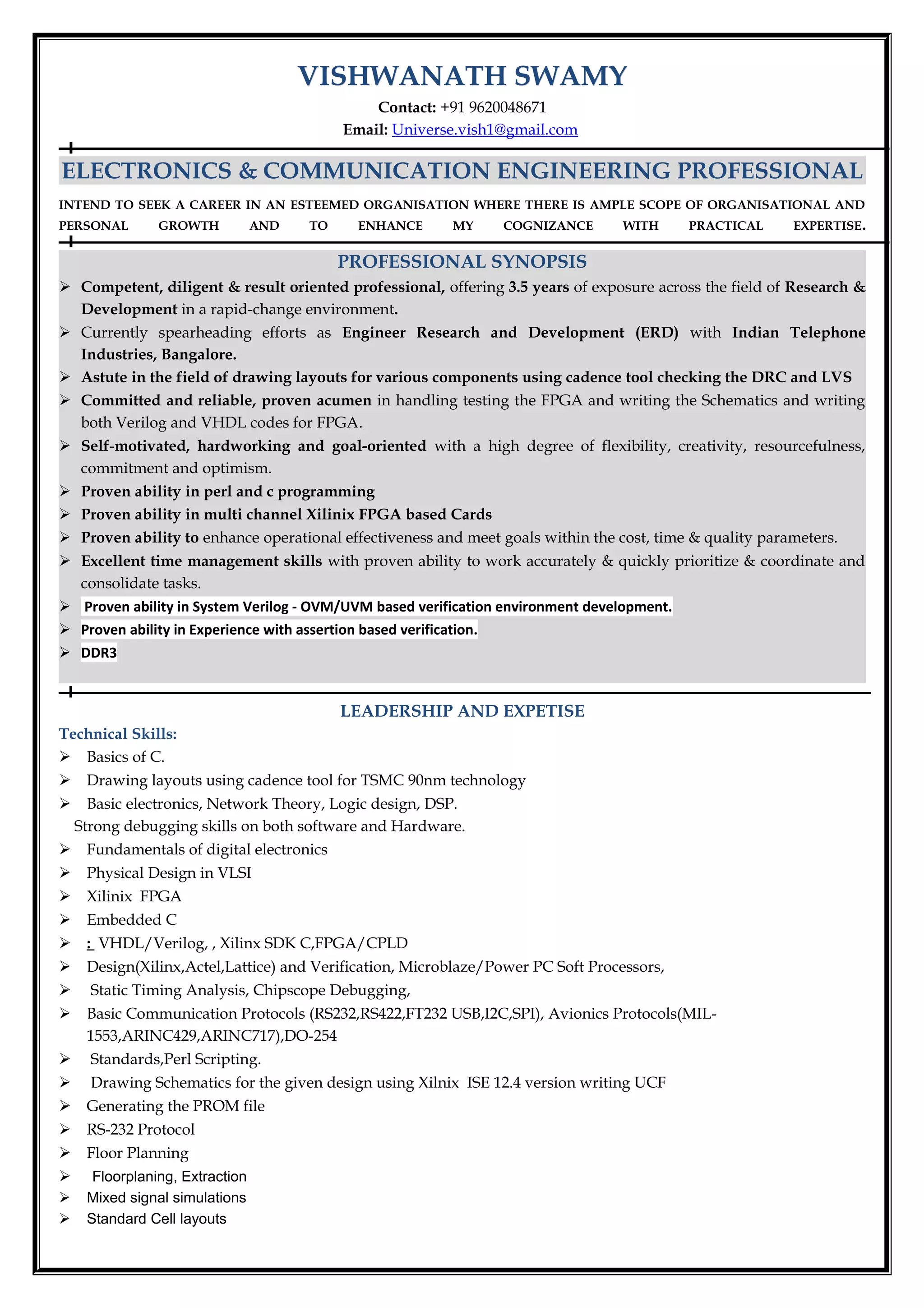
VISHWANATH SWAMYVISHWANATH SWAMY
Contact: +91 9620048671
Email: Universe.vish1@gmail.com
ELECTRONICS & COMMUNICATION ENGINEERING PROFESSIONAL
INTEND TO SEEK A CAREER IN AN ESTEEMED ORGANISATION WHERE THERE IS AMPLE SCOPE OF ORGANISATIONAL AND
PERSONAL GROWTH AND TO ENHANCE MY COGNIZANCE WITH PRACTICAL EXPERTISE.
PROFESSIONAL SYNOPSIS
 Competent, diligent & result oriented professional, offering 3.5 years of exposure across the field of Research &
Development in a rapid-change environment.
 Currently spearheading efforts as Engineer Research and Development (ERD) with Indian Telephone
Industries, Bangalore.
 Astute in the field of drawing layouts for various components using cadence tool checking the DRC and LVS
 Committed and reliable, proven acumen in handling testing the FPGA and writing the Schematics and writing
both Verilog and VHDL codes for FPGA.
 Self-motivated, hardworking and goal-oriented with a high degree of flexibility, creativity, resourcefulness,
commitment and optimism.
 Proven ability in perl and c programming
 Proven ability in multi channel Xilinix FPGA based Cards
 Proven ability to enhance operational effectiveness and meet goals within the cost, time & quality parameters.
 Excellent time management skills with proven ability to work accurately & quickly prioritize & coordinate and
consolidate tasks.
 Proven ability in System Verilog - OVM/UVM based verification environment development.
 Proven ability in Experience with assertion based verification.
 DDR3
LEADERSHIP AND EXPETISE
Technical Skills:
 Basics of C.
 Drawing layouts using cadence tool for TSMC 90nm technology
 Basic electronics, Network Theory, Logic design, DSP.
Strong debugging skills on both software and Hardware.
 Fundamentals of digital electronics
 Physical Design in VLSI
 Xilinix FPGA
 Embedded C
 : VHDL/Verilog, , Xilinx SDK C,FPGA/CPLD
 Design(Xilinx,Actel,Lattice) and Verification, Microblaze/Power PC Soft Processors,
 Static Timing Analysis, Chipscope Debugging,
 Basic Communication Protocols (RS232,RS422,FT232 USB,I2C,SPI), Avionics Protocols(MIL-
1553,ARINC429,ARINC717),DO-254
 Standards,Perl Scripting.
 Drawing Schematics for the given design using Xilnix ISE 12.4 version writing UCF
 Generating the PROM file
 RS-232 Protocol
 Floor Planning
 Floorplaning, Extraction
 Mixed signal simulations
 Standard Cell layouts
Key Skills:
 Self motivated ability to work in team and hard working nature with positive attitude.
 Quick learner, diligent, highly motivated, able to grasp new ideas, concepts and methods.
 Reliable, highly focused, result oriented, analytical and able to handle pressure with leadership qualities.
 Exceedingly detail oriented with a reputation for initiating solutions to problems.
 Function effectively as a team player and has the ability to work independently.
 Strong analytical skills; organized, easily assess situations and initiate appropriate interventions.
Soft Skills:
Analytical Skills ~ Decision Making Skills ~ Managerial Qualities ~ Monitoring Skills ~ Organizational Skills ~ Time
Management ~ Relationship Management ~ Presentation Skills ~ Coordination Skills ~ Learning Skills ~ Leadership Qualities
~ Interpersonal Skills ~ Result Oriented
PROJECT HIGHLIGHTS
Project Name: 1.NGN-BU
2..PROGRAMABLE PRIMARY MUX and ROAD TRAFFIC CONTROLLER USING PIC
Microcontrollers
3.Rainbow
Client: 1.Indian Army 2.Indian Railways
Duration: 1 ½ year for NGN-BU and ROAD TRAFFIC CONTROLLER for 1 year
Role: Grade -2 Engineer with ERD designation Engineer R & D
Client details: Indian Army and Indian Railways and Texaus Instruments
Project Description:
1.NGN BU(Next-Generation Bulk Network):in this project we programmed FPGA using
schematics and verilog/VHDL coding using Xilinix ISE Suite 12.4 version and drawn the layouts for
various digital circuits which are realized in terms of CMOS logic using Cadence Virtuso assura Tool
suite.Generated the PROM file and writing UCF files and fusing the same using (J-TAG)RS-232
protocol .
Duration:From May 2012 to March 2015
Roles Played :
As a a embedded engineer -embedded development I was involved in the following jobs
1.Writting the verilog and VHDL code for the given Hardware in Xilnix ISE 12.4 version
2.Compiling the code and writing UCF file for the given Design in xilinix ISE and Netlist verification
3.Generating the PROM file and fusing the code into the FPGA using Xilinix blaster using RS232
protocol and observing the spuratic activities on the CRO
4.Observing the waves forms on modelsim ISE and STA(Static Timing Analysis)
Skills used: system verilog , DDR3,UVM,Verilog RTL coding VHDL RTL coding , Analog
Design , Cadence Virtuoso tool,Xilnix 12.4 version,Modelsim,digital electronics PCBs,Cadence Virtuso,
assura,TSMC 90nm DRC and LVS ,LPC2468 processor,DRC,LVS TSMC 90nm TSMC 18nm,VI
editor ,Cadence Assura
Electronic Devices: Multimeter, CRO, Logic analyzer, VME Chasis.
Hardware Circuits Required
• RS 232.
• MPC-8548 Microprocessor
Virtex-5 FPGA
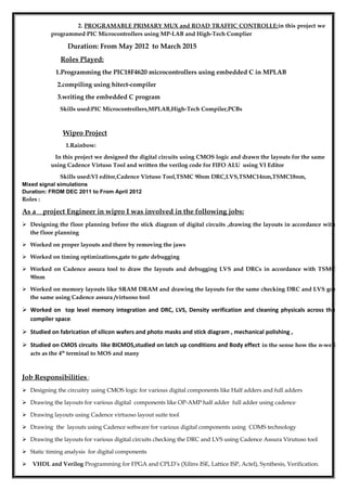
2. PROGRAMABLE PRIMARY MUX and ROAD TRAFFIC CONTROLLE:in this project we
programmed PIC Microcontrollers using MP-LAB and High-Tech Complier
Duration: From May 2012 to March 2015
Roles Played:
1.Programming the PIC18F4620 microcontrollers using embedded C in MPLAB
2.compiling using hitect-compiler
3.writing the embedded C program
Skills used:PIC Microcontrollers,MPLAB,High-Tech Compiler,PCBs
Wipro Project
1.Rainbow:
In this project we designed the digital circuits using CMOS logic and drawn the layouts for the same
using Cadence Virtuso Tool and written the verilog code for FIFO ALU using VI Editor
Skills used:VI editor,Cadence Virtuso Tool,TSMC 90nm DRC,LVS,TSMC14nm,TSMC18nm,
Mixed signal simulations
Duration: FROM DEC 2011 to From April 2012
Roles :
As a _ project Engineer in wipro I was involved in the following jobs:
 Designing the floor planning before the stick diagram of digital circuits ,drawing the layouts in accordance with
the floor planning
 Worked on proper layouts and there by removing the jaws
 Worked on timing optimizations,gate to gate debugging
 Worked on Cadence assura tool to draw the layouts and debugging LVS and DRCs in accordance with TSMC
90nm
 Worked on memory layouts like SRAM DRAM and drawing the layouts for the same checking DRC and LVS gor
the same using Cadence assura /virtuoso tool
 Worked on top level memory integration and DRC, LVS, Density verification and cleaning physicals across the
compiler space.
 Studied on fabrication of silicon wafers and photo masks and stick diagram , mechanical polishing ,
 Studied on CMOS circuits like BICMOS,studied on latch up conditions and Body effect in the sense how the n-well
acts as the 4th
terminal to MOS and many
Job Responsibilities :
 Designing the circuitry using CMOS logic for various digital components like Half adders and full adders
 Drawing the layouts for various digital components like OP-AMP half adder full adder using cadence
 Drawing layouts using Cadence virtuoso layout suite tool
 Drawing the layouts using Cadence software for various digital components using COMS technology
 Drawing the layouts for various digital circuits checking the DRC and LVS using Cadence Assura Virutuso tool
 Static timing analysis for digital components
 VHDL and Verilog Programming for FPGA and CPLD’s (Xilinx ISE, Lattice ISP, Actel), Synthesis, Verification.
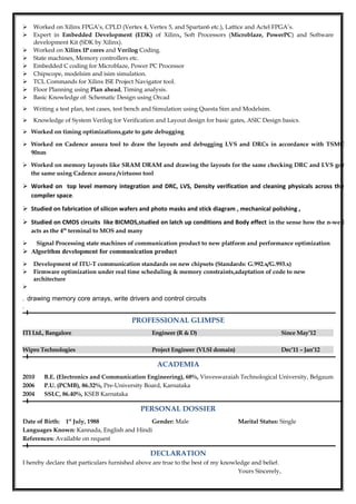
 Worked on Xilinx FPGA’s, CPLD (Vertex 4, Vertex 5, and Spartan6 etc.), Lattice and Actel FPGA’s.
 Expert in Embedded Development (EDK) of Xilinx, Soft Processors (Microblaze, PowerPC) and Software
development Kit (SDK by Xilinx).
 Worked on Xilinx IP cores and Verilog Coding.
 State machines, Memory controllers etc.
 Embedded C coding for Microblaze, Power PC Processor
 Chipscope, modelsim and isim simulation.
 TCL Commands for Xilinx ISE Project Navigator tool.
 Floor Planning using Plan ahead, Timing analysis.
 Basic Knowledge of: Schematic Design using Orcad
 Writing a test plan, test cases, test bench and Simulation using Questa Sim and Modelsim.
 Knowledge of System Verilog for Verification and Layout design for basic gates, ASIC Design basics.
 Worked on timing optimizations,gate to gate debugging
 Worked on Cadence assura tool to draw the layouts and debugging LVS and DRCs in accordance with TSMC
90nm
 Worked on memory layouts like SRAM DRAM and drawing the layouts for the same checking DRC and LVS gor
the same using Cadence assura /virtuoso tool
 Worked on top level memory integration and DRC, LVS, Density verification and cleaning physicals across the
compiler space.
 Studied on fabrication of silicon wafers and photo masks and stick diagram , mechanical polishing ,
 Studied on CMOS circuits like BICMOS,studied on latch up conditions and Body effect in the sense how the n-well
acts as the 4th
terminal to MOS and many
 Signal Processing state machines of communication product to new platform and performance optimization
 Algorithm development for communication product
 Development of ITU-T communication standards on new chipsets (Standards: G.992.x/G.993.x)
 Firmware optimization under real time scheduling & memory constraints,adaptation of code to new
architecture

. drawing memory core arrays, write drivers and control circuits
.
PROFESSIONAL GLIMPSE
ITI Ltd., Bangalore Engineer (R & D) Since May’12
Wipro Technologies Project Engineer (VLSI domain) Dec’11 – Jan’12
ACADEMIA
2010 B.E. (Electronics and Communication Engineering), 68%, Visveswaraiah Technological University, Belgaum
2006 P.U. (PCMB), 86.32%, Pre-University Board, Karnataka
2004 SSLC, 86.40%, KSEB Karnataka
PERSONAL DOSSIER
Date of Birth: 1st
July, 1988 Gender: Male Marital Status: Single
Languages Known: Kannada, English and Hindi
References: Available on request
DECLARATION
I hereby declare that particulars furnished above are true to the best of my knowledge and belief.
Yours Sincerely,
Date:
Place:
(VISHWANATH SWAMY)
Date:
Place:
(VISHWANATH SWAMY)

More Related Content

What's hot

Asic design lect1 2 august 28 2012
Asic design lect1 2 august 28 2012Asic design lect1 2 august 28 2012
Asic design lect1 2 august 28 2012babak danyal
 
Making of an Application Specific Integrated Circuit
Making of an Application Specific Integrated CircuitMaking of an Application Specific Integrated Circuit
Making of an Application Specific Integrated CircuitSWINDONSilicon
 
Zen 2: The AMD 7nm Energy-Efficient High-Performance x86-64 Microprocessor Core
Zen 2: The AMD 7nm Energy-Efficient High-Performance x86-64 Microprocessor CoreZen 2: The AMD 7nm Energy-Efficient High-Performance x86-64 Microprocessor Core
Zen 2: The AMD 7nm Energy-Efficient High-Performance x86-64 Microprocessor CoreAMD
 
Embedded system design process
Embedded system design processEmbedded system design process
Embedded system design processRayees CK
 
lect5_Stick_diagram_layout_rules
lect5_Stick_diagram_layout_ruleslect5_Stick_diagram_layout_rules
lect5_Stick_diagram_layout_rulesvein
 
Rs232 485 fundamental
Rs232 485 fundamentalRs232 485 fundamental
Rs232 485 fundamentalrounak077
 
AMD Chiplet Architecture for High-Performance Server and Desktop Products
AMD Chiplet Architecture for High-Performance Server and Desktop ProductsAMD Chiplet Architecture for High-Performance Server and Desktop Products
AMD Chiplet Architecture for High-Performance Server and Desktop ProductsAMD
 
VLSI
VLSI VLSI
VLSI So Ma
 
Vlsi physical design-notes
Vlsi physical design-notesVlsi physical design-notes
Vlsi physical design-notesDr.YNM
 
ASIC DESIGN : PLACEMENT
ASIC DESIGN : PLACEMENTASIC DESIGN : PLACEMENT
ASIC DESIGN : PLACEMENThelloactiva
 
Electronics Notice Board Notice board using Wi-Fi Report
Electronics Notice Board Notice board using Wi-Fi ReportElectronics Notice Board Notice board using Wi-Fi Report
Electronics Notice Board Notice board using Wi-Fi ReportVaibhav Pandey
 
Introduction to Embedded System I : Chapter 2 (2nd portion)
Introduction to Embedded System I : Chapter 2 (2nd portion)Introduction to Embedded System I : Chapter 2 (2nd portion)
Introduction to Embedded System I : Chapter 2 (2nd portion)Moe Moe Myint
 
Intellectual property in vlsi
Intellectual property in vlsiIntellectual property in vlsi
Intellectual property in vlsiSaransh Choudhary
 

What's hot (20)

Asic design lect1 2 august 28 2012
Asic design lect1 2 august 28 2012Asic design lect1 2 august 28 2012
Asic design lect1 2 august 28 2012
 
Multi chip module
Multi chip moduleMulti chip module
Multi chip module
 
Making of an Application Specific Integrated Circuit
Making of an Application Specific Integrated CircuitMaking of an Application Specific Integrated Circuit
Making of an Application Specific Integrated Circuit
 
Zen 2: The AMD 7nm Energy-Efficient High-Performance x86-64 Microprocessor Core
Zen 2: The AMD 7nm Energy-Efficient High-Performance x86-64 Microprocessor CoreZen 2: The AMD 7nm Energy-Efficient High-Performance x86-64 Microprocessor Core
Zen 2: The AMD 7nm Energy-Efficient High-Performance x86-64 Microprocessor Core
 
Embedded system design process
Embedded system design processEmbedded system design process
Embedded system design process
 
PowerPlanning.pdf
PowerPlanning.pdfPowerPlanning.pdf
PowerPlanning.pdf
 
lect5_Stick_diagram_layout_rules
lect5_Stick_diagram_layout_ruleslect5_Stick_diagram_layout_rules
lect5_Stick_diagram_layout_rules
 
Rs232 485 fundamental
Rs232 485 fundamentalRs232 485 fundamental
Rs232 485 fundamental
 
AMD Chiplet Architecture for High-Performance Server and Desktop Products
AMD Chiplet Architecture for High-Performance Server and Desktop ProductsAMD Chiplet Architecture for High-Performance Server and Desktop Products
AMD Chiplet Architecture for High-Performance Server and Desktop Products
 
Latest Resume C#,C++ Developer
Latest Resume C#,C++ DeveloperLatest Resume C#,C++ Developer
Latest Resume C#,C++ Developer
 
VLSI
VLSI VLSI
VLSI
 
Vlsi physical design-notes
Vlsi physical design-notesVlsi physical design-notes
Vlsi physical design-notes
 
Modbus protocol
Modbus protocolModbus protocol
Modbus protocol
 
ASIC DESIGN : PLACEMENT
ASIC DESIGN : PLACEMENTASIC DESIGN : PLACEMENT
ASIC DESIGN : PLACEMENT
 
Lect01 flow
Lect01 flowLect01 flow
Lect01 flow
 
R18 b.tech 3 2 ece syllabus
R18 b.tech 3 2 ece syllabusR18 b.tech 3 2 ece syllabus
R18 b.tech 3 2 ece syllabus
 
Asic pd
Asic pdAsic pd
Asic pd
 
Electronics Notice Board Notice board using Wi-Fi Report
Electronics Notice Board Notice board using Wi-Fi ReportElectronics Notice Board Notice board using Wi-Fi Report
Electronics Notice Board Notice board using Wi-Fi Report
 
Introduction to Embedded System I : Chapter 2 (2nd portion)
Introduction to Embedded System I : Chapter 2 (2nd portion)Introduction to Embedded System I : Chapter 2 (2nd portion)
Introduction to Embedded System I : Chapter 2 (2nd portion)
 
Intellectual property in vlsi
Intellectual property in vlsiIntellectual property in vlsi
Intellectual property in vlsi
 

Viewers also liked

Resume_Anurag_Design_Verification_2+_yrs
Resume_Anurag_Design_Verification_2+_yrsResume_Anurag_Design_Verification_2+_yrs
Resume_Anurag_Design_Verification_2+_yrsANURAG KAVADANA
 
Gayathri_Physical_Design_Intel
Gayathri_Physical_Design_IntelGayathri_Physical_Design_Intel
Gayathri_Physical_Design_Intelgaya3vijay
 
Final_Resume_Rev L
Final_Resume_Rev LFinal_Resume_Rev L
Final_Resume_Rev LHerve Pierre
 
CV_NguyenVanHai
CV_NguyenVanHaiCV_NguyenVanHai
CV_NguyenVanHaiHai Nguyen
 
Darshan Dehuniya - Resume - ASIC Verification Engineer (1)
Darshan Dehuniya - Resume - ASIC Verification Engineer  (1)Darshan Dehuniya - Resume - ASIC Verification Engineer  (1)
Darshan Dehuniya - Resume - ASIC Verification Engineer (1)Darshan Dehuniya
 

Viewers also liked (11)

DrE.N.Ganesh_recent resume
DrE.N.Ganesh_recent resumeDrE.N.Ganesh_recent resume
DrE.N.Ganesh_recent resume
 
Resume_Anurag_Design_Verification_2+_yrs
Resume_Anurag_Design_Verification_2+_yrsResume_Anurag_Design_Verification_2+_yrs
Resume_Anurag_Design_Verification_2+_yrs
 
Gayathri_Physical_Design_Intel
Gayathri_Physical_Design_IntelGayathri_Physical_Design_Intel
Gayathri_Physical_Design_Intel
 
Resume srishail upadhye
Resume srishail upadhyeResume srishail upadhye
Resume srishail upadhye
 
Final_Resume_Rev L
Final_Resume_Rev LFinal_Resume_Rev L
Final_Resume_Rev L
 
RRader_Resume
RRader_ResumeRRader_Resume
RRader_Resume
 
Shannon Griffiths Resume
Shannon Griffiths ResumeShannon Griffiths Resume
Shannon Griffiths Resume
 
My resume
My resumeMy resume
My resume
 
Basavanthrao_resume_vlsi
Basavanthrao_resume_vlsiBasavanthrao_resume_vlsi
Basavanthrao_resume_vlsi
 
CV_NguyenVanHai
CV_NguyenVanHaiCV_NguyenVanHai
CV_NguyenVanHai
 
Darshan Dehuniya - Resume - ASIC Verification Engineer (1)
Darshan Dehuniya - Resume - ASIC Verification Engineer  (1)Darshan Dehuniya - Resume - ASIC Verification Engineer  (1)
Darshan Dehuniya - Resume - ASIC Verification Engineer (1)
 

Similar to verification resume

Similar to verification resume (20)

Detailed Cv
Detailed CvDetailed Cv
Detailed Cv
 
Bindu_Resume
Bindu_ResumeBindu_Resume
Bindu_Resume
 
Viswateja_Nemani
Viswateja_NemaniViswateja_Nemani
Viswateja_Nemani
 
Resume-Zhuyu
Resume-ZhuyuResume-Zhuyu
Resume-Zhuyu
 
Resume
ResumeResume
Resume
 
CV-RENJINIK-27062016
CV-RENJINIK-27062016CV-RENJINIK-27062016
CV-RENJINIK-27062016
 
Jay_Vicory_Resume_2018
Jay_Vicory_Resume_2018Jay_Vicory_Resume_2018
Jay_Vicory_Resume_2018
 
Surya resume
Surya resumeSurya resume
Surya resume
 
Hardware Design engineer
Hardware Design engineerHardware Design engineer
Hardware Design engineer
 
Resume16AugV
Resume16AugVResume16AugV
Resume16AugV
 
Resume_updated
Resume_updatedResume_updated
Resume_updated
 
OliverStoneSWResume2015-05
OliverStoneSWResume2015-05OliverStoneSWResume2015-05
OliverStoneSWResume2015-05
 
Resume_8years-Exp_Embedded
Resume_8years-Exp_EmbeddedResume_8years-Exp_Embedded
Resume_8years-Exp_Embedded
 
Software analyst resume
Software analyst resumeSoftware analyst resume
Software analyst resume
 
Resume_01
Resume_01Resume_01
Resume_01
 
SoC~FPGA~ASIC~Embedded
SoC~FPGA~ASIC~EmbeddedSoC~FPGA~ASIC~Embedded
SoC~FPGA~ASIC~Embedded
 
Sudhakar_Resume
Sudhakar_ResumeSudhakar_Resume
Sudhakar_Resume
 
Curriculum_Vitae_lavanya_doc
Curriculum_Vitae_lavanya_docCurriculum_Vitae_lavanya_doc
Curriculum_Vitae_lavanya_doc
 
JD Role Type Slides - 12.2022.pdf
JD Role Type Slides - 12.2022.pdfJD Role Type Slides - 12.2022.pdf
JD Role Type Slides - 12.2022.pdf
 
CV_Swapnil_Deshmukh
CV_Swapnil_DeshmukhCV_Swapnil_Deshmukh
CV_Swapnil_Deshmukh
 

verification resume

  • 1. VISHWANATH SWAMYVISHWANATH SWAMY Contact: +91 9620048671 Email: Universe.vish1@gmail.com ELECTRONICS & COMMUNICATION ENGINEERING PROFESSIONAL INTEND TO SEEK A CAREER IN AN ESTEEMED ORGANISATION WHERE THERE IS AMPLE SCOPE OF ORGANISATIONAL AND PERSONAL GROWTH AND TO ENHANCE MY COGNIZANCE WITH PRACTICAL EXPERTISE. PROFESSIONAL SYNOPSIS  Competent, diligent & result oriented professional, offering 3.5 years of exposure across the field of Research & Development in a rapid-change environment.  Currently spearheading efforts as Engineer Research and Development (ERD) with Indian Telephone Industries, Bangalore.  Astute in the field of drawing layouts for various components using cadence tool checking the DRC and LVS  Committed and reliable, proven acumen in handling testing the FPGA and writing the Schematics and writing both Verilog and VHDL codes for FPGA.  Self-motivated, hardworking and goal-oriented with a high degree of flexibility, creativity, resourcefulness, commitment and optimism.  Proven ability in perl and c programming  Proven ability in multi channel Xilinix FPGA based Cards  Proven ability to enhance operational effectiveness and meet goals within the cost, time & quality parameters.  Excellent time management skills with proven ability to work accurately & quickly prioritize & coordinate and consolidate tasks.  Proven ability in System Verilog - OVM/UVM based verification environment development.  Proven ability in Experience with assertion based verification.  DDR3 LEADERSHIP AND EXPETISE Technical Skills:  Basics of C.  Drawing layouts using cadence tool for TSMC 90nm technology  Basic electronics, Network Theory, Logic design, DSP. Strong debugging skills on both software and Hardware.  Fundamentals of digital electronics  Physical Design in VLSI  Xilinix FPGA  Embedded C  : VHDL/Verilog, , Xilinx SDK C,FPGA/CPLD  Design(Xilinx,Actel,Lattice) and Verification, Microblaze/Power PC Soft Processors,  Static Timing Analysis, Chipscope Debugging,  Basic Communication Protocols (RS232,RS422,FT232 USB,I2C,SPI), Avionics Protocols(MIL- 1553,ARINC429,ARINC717),DO-254  Standards,Perl Scripting.  Drawing Schematics for the given design using Xilnix ISE 12.4 version writing UCF  Generating the PROM file  RS-232 Protocol  Floor Planning  Floorplaning, Extraction  Mixed signal simulations  Standard Cell layouts
  • 2. Key Skills:  Self motivated ability to work in team and hard working nature with positive attitude.  Quick learner, diligent, highly motivated, able to grasp new ideas, concepts and methods.  Reliable, highly focused, result oriented, analytical and able to handle pressure with leadership qualities.  Exceedingly detail oriented with a reputation for initiating solutions to problems.  Function effectively as a team player and has the ability to work independently.  Strong analytical skills; organized, easily assess situations and initiate appropriate interventions. Soft Skills: Analytical Skills ~ Decision Making Skills ~ Managerial Qualities ~ Monitoring Skills ~ Organizational Skills ~ Time Management ~ Relationship Management ~ Presentation Skills ~ Coordination Skills ~ Learning Skills ~ Leadership Qualities ~ Interpersonal Skills ~ Result Oriented PROJECT HIGHLIGHTS Project Name: 1.NGN-BU 2..PROGRAMABLE PRIMARY MUX and ROAD TRAFFIC CONTROLLER USING PIC Microcontrollers 3.Rainbow Client: 1.Indian Army 2.Indian Railways Duration: 1 ½ year for NGN-BU and ROAD TRAFFIC CONTROLLER for 1 year Role: Grade -2 Engineer with ERD designation Engineer R & D Client details: Indian Army and Indian Railways and Texaus Instruments Project Description: 1.NGN BU(Next-Generation Bulk Network):in this project we programmed FPGA using schematics and verilog/VHDL coding using Xilinix ISE Suite 12.4 version and drawn the layouts for various digital circuits which are realized in terms of CMOS logic using Cadence Virtuso assura Tool suite.Generated the PROM file and writing UCF files and fusing the same using (J-TAG)RS-232 protocol . Duration:From May 2012 to March 2015 Roles Played : As a a embedded engineer -embedded development I was involved in the following jobs 1.Writting the verilog and VHDL code for the given Hardware in Xilnix ISE 12.4 version 2.Compiling the code and writing UCF file for the given Design in xilinix ISE and Netlist verification 3.Generating the PROM file and fusing the code into the FPGA using Xilinix blaster using RS232 protocol and observing the spuratic activities on the CRO 4.Observing the waves forms on modelsim ISE and STA(Static Timing Analysis) Skills used: system verilog , DDR3,UVM,Verilog RTL coding VHDL RTL coding , Analog Design , Cadence Virtuoso tool,Xilnix 12.4 version,Modelsim,digital electronics PCBs,Cadence Virtuso, assura,TSMC 90nm DRC and LVS ,LPC2468 processor,DRC,LVS TSMC 90nm TSMC 18nm,VI editor ,Cadence Assura Electronic Devices: Multimeter, CRO, Logic analyzer, VME Chasis. Hardware Circuits Required • RS 232. • MPC-8548 Microprocessor Virtex-5 FPGA
  • 3. 2. PROGRAMABLE PRIMARY MUX and ROAD TRAFFIC CONTROLLE:in this project we programmed PIC Microcontrollers using MP-LAB and High-Tech Complier Duration: From May 2012 to March 2015 Roles Played: 1.Programming the PIC18F4620 microcontrollers using embedded C in MPLAB 2.compiling using hitect-compiler 3.writing the embedded C program Skills used:PIC Microcontrollers,MPLAB,High-Tech Compiler,PCBs Wipro Project 1.Rainbow: In this project we designed the digital circuits using CMOS logic and drawn the layouts for the same using Cadence Virtuso Tool and written the verilog code for FIFO ALU using VI Editor Skills used:VI editor,Cadence Virtuso Tool,TSMC 90nm DRC,LVS,TSMC14nm,TSMC18nm, Mixed signal simulations Duration: FROM DEC 2011 to From April 2012 Roles : As a _ project Engineer in wipro I was involved in the following jobs:  Designing the floor planning before the stick diagram of digital circuits ,drawing the layouts in accordance with the floor planning  Worked on proper layouts and there by removing the jaws  Worked on timing optimizations,gate to gate debugging  Worked on Cadence assura tool to draw the layouts and debugging LVS and DRCs in accordance with TSMC 90nm  Worked on memory layouts like SRAM DRAM and drawing the layouts for the same checking DRC and LVS gor the same using Cadence assura /virtuoso tool  Worked on top level memory integration and DRC, LVS, Density verification and cleaning physicals across the compiler space.  Studied on fabrication of silicon wafers and photo masks and stick diagram , mechanical polishing ,  Studied on CMOS circuits like BICMOS,studied on latch up conditions and Body effect in the sense how the n-well acts as the 4th terminal to MOS and many Job Responsibilities :  Designing the circuitry using CMOS logic for various digital components like Half adders and full adders  Drawing the layouts for various digital components like OP-AMP half adder full adder using cadence  Drawing layouts using Cadence virtuoso layout suite tool  Drawing the layouts using Cadence software for various digital components using COMS technology  Drawing the layouts for various digital circuits checking the DRC and LVS using Cadence Assura Virutuso tool  Static timing analysis for digital components  VHDL and Verilog Programming for FPGA and CPLD’s (Xilinx ISE, Lattice ISP, Actel), Synthesis, Verification.
  • 4.  Worked on Xilinx FPGA’s, CPLD (Vertex 4, Vertex 5, and Spartan6 etc.), Lattice and Actel FPGA’s.  Expert in Embedded Development (EDK) of Xilinx, Soft Processors (Microblaze, PowerPC) and Software development Kit (SDK by Xilinx).  Worked on Xilinx IP cores and Verilog Coding.  State machines, Memory controllers etc.  Embedded C coding for Microblaze, Power PC Processor  Chipscope, modelsim and isim simulation.  TCL Commands for Xilinx ISE Project Navigator tool.  Floor Planning using Plan ahead, Timing analysis.  Basic Knowledge of: Schematic Design using Orcad  Writing a test plan, test cases, test bench and Simulation using Questa Sim and Modelsim.  Knowledge of System Verilog for Verification and Layout design for basic gates, ASIC Design basics.  Worked on timing optimizations,gate to gate debugging  Worked on Cadence assura tool to draw the layouts and debugging LVS and DRCs in accordance with TSMC 90nm  Worked on memory layouts like SRAM DRAM and drawing the layouts for the same checking DRC and LVS gor the same using Cadence assura /virtuoso tool  Worked on top level memory integration and DRC, LVS, Density verification and cleaning physicals across the compiler space.  Studied on fabrication of silicon wafers and photo masks and stick diagram , mechanical polishing ,  Studied on CMOS circuits like BICMOS,studied on latch up conditions and Body effect in the sense how the n-well acts as the 4th terminal to MOS and many  Signal Processing state machines of communication product to new platform and performance optimization  Algorithm development for communication product  Development of ITU-T communication standards on new chipsets (Standards: G.992.x/G.993.x)  Firmware optimization under real time scheduling & memory constraints,adaptation of code to new architecture  . drawing memory core arrays, write drivers and control circuits . PROFESSIONAL GLIMPSE ITI Ltd., Bangalore Engineer (R & D) Since May’12 Wipro Technologies Project Engineer (VLSI domain) Dec’11 – Jan’12 ACADEMIA 2010 B.E. (Electronics and Communication Engineering), 68%, Visveswaraiah Technological University, Belgaum 2006 P.U. (PCMB), 86.32%, Pre-University Board, Karnataka 2004 SSLC, 86.40%, KSEB Karnataka PERSONAL DOSSIER Date of Birth: 1st July, 1988 Gender: Male Marital Status: Single Languages Known: Kannada, English and Hindi References: Available on request DECLARATION I hereby declare that particulars furnished above are true to the best of my knowledge and belief. Yours Sincerely,