The document describes designing and simulating various combinational circuits using Verilog HDL. It includes the design of an 8-bit adder, 4-bit multiplier, 3-to-8 address decoder, and 2-to-1 multiplexer. Verilog code and test benches are provided for each circuit. The circuits are simulated and waveforms are generated to verify the design and functionality.
![CODING:
Date: a) 8 BIT ADDER
1 BIT ADDER
Verilog Code:
module fulladder(sum,carry,a,b,cin);
input a,b;
input cin;
output sum;
output carry;
assign sum=a^b^cin;
assign carry=((a&b)|(b&cin)|(cin&a));
endmodule
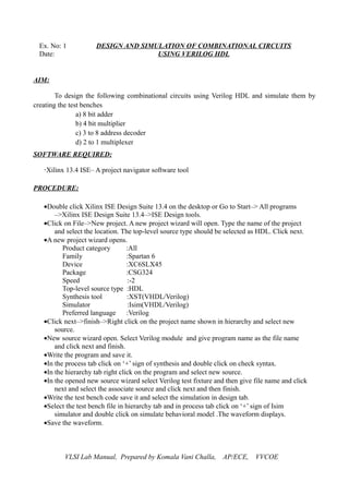
8 BIT ADDER
Verilog Code:
module adder8bit(sum,carry,a,b,cin);
input [7:0] a,b;
input cin;
output [7:0] sum;
output carry;
wire c1,c2,c3,c4,c5,c6,c7;
fulladder fa0(sum[0],c1,a[0],b[0],cin);
fulladder fa1(sum[1],c2,a[1],b[1],c1);
fulladder fa2(sum[2],c3,a[2],b[2],c2);
fulladder fa3(sum[3],c4,a[3],b[3],c3);
fulladder fa4(sum[4],c5,a[4],b[4],c4);
fulladder fa5(sum[5],c6,a[5],b[5],c5);
fulladder fa6(sum[6],c7,a[6],b[6],c6);
fulladder fa7(sum[7],carry,a[7],b[7],c7);
endmodule
Test Bench:
module fatb;
// Inputs
reg [7:0] a;
reg [7:0] b;
reg cin;
// Outputs
wire [7:0] sum;
wire carry;
// Instantiate the Unit Under Test (UUT)
fa8bit uut (
.sum(sum),
.carry(carry),
.a(a),
.b(b),
.cin(cin)
);
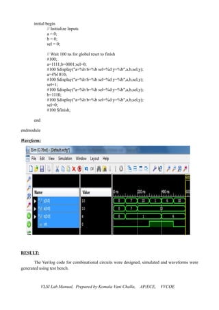
initial begin
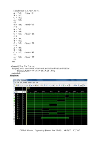
VLSI Lab Manual, Prepared by Komala Vani Challa, AP/ECE, VVCOE](https://image.slidesharecdn.com/vlsi-1f-141115005459-conversion-gate01/85/Vlsi-lab-manual-exp-1-2-320.jpg)
![Date: b) 4 BIT MULTIPLIER:
Verilog Code:
module mul4bit(a,b,out);
input [3:0] a;
input [3:0] b;
output [7:0] out;
reg [7:0] out;
always @ (a or b)
begin
out <= a*b;
end
endmodule
Testbench:
module multb;
// Inputs
reg [3:0] a;
reg [3:0] b;
// Outputs
wire [7:0] out;
// Instantiate the Unit Under Test (UUT)
mul4bit uut (
.a(a),
.b(b),
.out(out)
);
initial begin
a = 0;
b = 0;
// Wait 100 ns for global reset to finish
#100 $display("out=%b",out);
a=4'b0000;b=4'b1100;
#100 $display("out=%b",out);
a=4'b1000;
#100 $display("out=%b",out);
a=4'b1010;b=4'b0101;
#100 $display("out=%b",out);
#100 $finish;
end
endmodule
Waveform:
VLSI Lab Manual, Prepared by Komala Vani Challa, AP/ECE, VVCOE](https://image.slidesharecdn.com/vlsi-1f-141115005459-conversion-gate01/85/Vlsi-lab-manual-exp-1-4-320.jpg)
![Date: d) MULTIPLEXER
2 to 1 Multiplexer Logic Diagram:
Fig. 2 to 1 Mux
Verilog Code:
module mux(y,a,b,sel);
input [3:0] a,b;
input sel;
output [3:0] y;
reg [3:0] y;
always @(a or b or sel)
if (sel == 1'b0)
y=a;
else
y=b;
endmodule
Testbench:
module muxtb;
// Inputs
reg [3:0] a;
reg [3:0] b;
reg sel;
// Outputs
wire [3:0] y;
// Instantiate the Unit Under Test (UUT)
mux uut (
.y(y),
.a(a),
.b(b),
.sel(sel)
);
VLSI Lab Manual, Prepared by Komala Vani Challa, AP/ECE, VVCOE](https://image.slidesharecdn.com/vlsi-1f-141115005459-conversion-gate01/85/Vlsi-lab-manual-exp-1-7-320.jpg)