Zvi Kohavi and Niraj K. Jha
1
Logical Design
2
Design with Basic Logic Gates
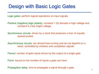
Logic gates: perform logical operations on input signals
Positive (negative) logic polarity: constant 1 (0) denotes a high voltage and
constant 0 a low (high) voltage
Synchronous circuits: driven by a clock that produces a train of equally
spaced pulses
Asynchronous circuits: are almost free-running and do not depend on a
clock; controlled by initiation and completion signals
Fanout: number of gate inputs driven by the output of a single gate
Fanin: bound on the number of inputs a gate can have
Propagation delay: time to propagate a signal through a gate
3
Analysis of Combinational Circuits
Circuit analysis: determine the Boolean function that describes the circuit
• Done by tracing the output of each gate, starting from circuit inputs and
continuing towards each circuit output
Example: a multi-level realization of a full binary adder
(A + B + C)[AB + C(A + B)]
AB
B
AB + (A + B)C
A
ABC
(A + B)C
C
A + B + C
A + B
C0
S
C0 = AB + (A + B)C
= AB + AC + BC
S = (A + B + C)[AB + (A + B)C]’ + ABC
= (A + B + C)(A’ + B’)(A’ + C’)(B’ + C’)
+ ABC
= AB’C’ + A’BC’ + A’B’C + ABC
= A B C
+ +
4
Simple Design Problems
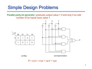
Parallel parity-bit generator: produces output value 1 if and only if an odd
number of its inputs have value 1
P = x’y’z + x’yz’ + xy’z’ + xyz
0
0 1
1 0
1
xy
z
0
1
00 01 11 10
1
0
z x
y
P
(a) Map. (b) Implementation.
5
Simple Design Problems (Contd.)
Serial-to-parallel converter: distributes a sequence of binary digits on a
serial input to a set of different outputs, as specified by external
control signals
C1
C2
L1
L4
L3
L2
x
6
Logic Design with Integrated Circuits
Small scale integration (SSI): integrated circuit packages containing a few
gates; e.g., AND, OR, NOT, NAND, NOR, XOR
Medium scale integration (MSI): packages containing up to about 100
gates; e.g., code converters, adders
Large scale integration (LSI): packages containing thousands of gates;
arithmetic unit
Very large scale integration (VLSI): packages with millions of gates
7
Comparators
n-bit comparator: compares the magnitude of two numbers X and Y, and
has three outputs f1, f2, and f3
• f1 = 1 iff X > Y
• f2 = 1 iff X = Y
• f3 = 1 iff X < Y
x1
f1
y2
x2
y1
x1
y1
00 01 11 10
(b) Map for f1, f2, and f3.
00
01
11
10
3
x1x2
y1y2
2
3
3
1
2
3
3
1
1
2
1
1
1
3
2
x1
f3
f2
f1
y2
y1
x2
(a) Block diagram.
(c) Circuit for f1.
2-bit comparator
f1 = x1x2y2’ + x2y1’y2’ + x1y1’
= (x1 + y1’)x2y2’ + x1y1’
f2 = x1’x2’y1’y2’ + x1’x2y1’y2 +
x1x2’y1y2’ + x1x2y1y2
= x1’y1’(x2’y2’ + x2y2) +
x1y1(x2’y2’ + x2y2)
= (x1’y1’ + x1y1)(x2’y2’ + x2y2)
f3 = x2’y1y2 + x1’x2’y2 + x1’y1
= x2’y2(y1 + x1’) + x1’y1
8
4-bit/12-bit Comparators
Four-bit comparator: 11 inputs (four for X, four for Y, and three connected
to outputs f1, f2 and f3 of the preceding stage)
12-bit comparator:
x1
f3
f2
f1
y4
y1
x4
(a) A 4-bit comparator.
Inputs from
preceding
stage
x1
f3
f2
f1
y4
y1
x4 y8
y5 y12
y9
x12
x9
x8
x5
>
=
<
>
=
<
>
=
<
>
=
<
>
=
<
>
=
<
>
=
<
>
=
<
(b) A 12-bit comparator.
0
0
1
9
Data Selectors
Multiplexer: electronic switch that connects one of n inputs to the output
Data selector: application of multiplexer
• n data input lines, D0, D1, …, Dn-1
• m select digit inputs s0, s1, …, sm-1
• 1 output
Enable
(a) Block diagram.
Select
number
Data inputs
D7 D0
D1
D2
D3
D4
D5
D6
s2
s0
s1
z
z
z
(b) Logic diagram.
s0
s1
s2 D0
D1
D2
D3
D4
D5
D6
D7 Enable
Select number Data inputs
10
Implementing Switching Functions with
Data Selectors
Data selectors: can implement arbitrary switching functions
Example: implementing two-variable functions
z
s
D1 D0
Enable
z = sD1 + s D0
If s = A, B = D0, and
B = D1, then z = A B.
If s = A, D0 = 1, and
D1 = B , then z = A + B.
+
11
Implementing Switching Functions with
Data Selectors (Contd.)
To implement an n-variable function: a data selector with n-1 select inputs
and 2n-1 data inputs
Implementing three-variable functions:
z = s2’s1’D0 + s2’s1D1 + s2s1’D2 + s2s1D3
Example: s1 = A, s2 = B, D0 = C, D1 = 1, D2 = 0, D3 = C’
z = A’B’C + AB’ + ABC’
= AC’ + B’C
General case: Assign n-1 variables to the select inputs and last variable
and constants 0 and 1 to the data inputs such that desired
function results
12
Priority Encoders
Priority encoder: n input lines and log2n output lines
• Input lines represent units that may request service
• When inputs pi and pj, such that i > j, request service simultaneously, line
pi has priority over line pj
• Encoder produces a binary output code indicating which of the input lines
requesting service has the highest priority
Example: Eight-input, three-output priority encoder
z4 = p4p5’p6’p7’ + p5p6’p7’ + p6p7’ + p7 = p4 + p5 + p6 + p7
z2 = p2p3’p4’p5’p6’p7’ + p3p4’p5’p6’p7’ + p6p7’ + p7 = p2p4’p5’ + p3p4’p5’ + p6 + p7
z1 = p1p2’p3’p4’p5’p6’p7’ + p3p4’p5’p6’p7’ + p5p6’p7’ + p7 = p1p2’p4’p6’ + p3p4’p6’ + p5p6’ + p7
Enable
z1
p0
z4
z0
(a) Block diagram.
Priority
encoder
z2
p7
p6
p5
p4
p3
p1
p2
z4
p7
(b) Truth table.
z2
p6
0 0 0 0
0
0 0
1
0
1
1 0 1 0
1
1
1
1
0
1 1
0
0
0
1
0 0
0
0 1
0
1 0
1
0
Input lines Outputs
p5
p4 z1
0 0
0
0
0
0
0
0
0
0
0
0
0
0
0
0
0
0
0
1
1
1
1
1
1
p3
p2
p1
p0
13
Priority Encoders (Contd.)
(c) Logic diagram.
z1
Enable
z4
z2
p7
p6
p5
p4
p3
p2
p1
p0
z0
Request
indicator
14
Decoders
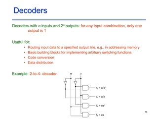
Decoders with n inputs and 2n outputs: for any input combination, only one
output is 1
Useful for:
• Routing input data to a specified output line, e.g., in addressing memory
• Basic building blocks for implementing arbitrary switching functions
• Code conversion
• Data distribution
Example: 2-to-4- decoder x
w
f0 = w x
f3 = wx
f2 = wx
f1 = w x
15
Decoders (Contd.)
Example: 4-to-16 decoder made of two 2-to-4 decoders and a gate-
switching matrix
x
w
y
f0
z
f0
f12
f8
f4
f1
f13
f9
f5
f2
f14
f10
f6
f3
f15
f11
f7
2-to-4
2-to-4
f3
f2
f1
f0
f3
f2
f1
16
Decimal Decoder
BCD-to-decimal: 4-to-16 decoder made of two 2-to-4 decoders and a gate-
switching matrix
Enable
f1
w f0
f4
f3
z
y
x
(a) Block diagram. (b) Map.
f9
00 01 11 10
00
01
11
10
wx
yz
Decimal
decoder
f9
f2
f8
f7
f6
f5
f0
f1
f2
f3
f4
f5
f6
f7
f8
x y
f0
f3
f2
f1
(c) Logic diagram.
f4
f7
f6
f5
f9
f8
w z
Enable
17
Decimal Decoder (Contd.)
Implementation using a partial-gate matrix:
w
w
x
x
w
x
y
f3
f7
z y
f0
f4
z
y
f2
f6
z y
f1
f5
z
f9 f8
18
Implementing Arbitrary Switching
Functions
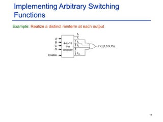
Example: Realize a distinct minterm at each output
f15
f1
A
f0
f9
f5
D
C
B 4-to-16
line
decoder
Enable
f = (1,5,9,15)
19
Demultiplexers
Demultiplexers: decoder with1 data input and n address inputs
• Directs input to any one of the 2n outputs
Example: A 4-output demultiplexer
Enable
2n
outputs
n-bit address
Data input
C1
C2
L1
L4
L3
L2
x
20
Seven-segment Display
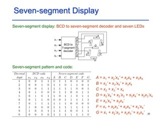
Seven-segment display: BCD to seven-segment decoder and seven LEDs
Seven-segment pattern and code:
D
E
x1
C
A
B
x4
x3
x2 BCD to
7-segment
decoder
G
F
A
B
C
D
E
F
G
A = x1 + x2’x4’ + x2x4 + x3x4
B = x2’ + x3’x4’ + x3x4
C = x2 + x3’ + x4
D = x2’x4’ + x2’x3 + x3x4’ + x2x3’x4
E = x2’x4’ + x3x4’
F = x1 + x2x3’ + x2x4’ + x3’x4’
G = x1 + x2’x3 + x2x3’ + x3x4’
21
Sine Generators
Combinational sine generators: for fast and repeated evaluation of sine
• Input: angle in radians converted to binary
• Output: sine in binary
z1 = x1’x2 + x1x2’ + x2x3’ + x1’x3x4
z2 = x1x2’ + x3x4’ + x1’x2x4
z3 = x3x4’ + x2x3 + x2x4’ +
x2’x3’x4 + x1x4’
z4 = x2’x3’x4 + x2x3’x4’ + x1x2’x3’ +
x1x3x4 + x1’x2x4
z1
x4
(a) Truth table.
z2
x3
0 0 0 0
0
0 0 1 0 1
1
1
0 1 0
1
1
1 1
1
1 0
1 1 0
1
0
0
0
1
0 1
0
0
1
0 1
1
1
0
Angle x sin( x)
x2
x1 z4
z3
0
0
0
0
0
0
0
0
0
0
0
0
0
0
0
0
0
0
0
0
0
0
1
1
1
1
1
1
1
1
1
1
0
0
0
0
1
1
1
1
1
1
1
1
1
1
1
1
1
1
1
1
1
1
1
1
1
1
1
1
1
1
1
1
1
1
1
1
1
1
1
1
1
1
1
1
1
1
0
0
0
0
0
0
0
0
0
0
Sine
generator
x3
z1
x2
x1
(b) Block diagram.
x4 z4
z3
z2
sin( x)
22
NAND/NOR Circuits
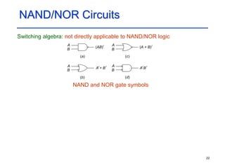
Switching algebra: not directly applicable to NAND/NOR logic
NAND and NOR gate symbols
A
A
A
(AB)
B
B
(A + B)
(a)
A
B
A + B A B
B
(d)
(b)
(c)
23
Analysis of NAND/NOR Networks
Example: circles (inversions) at both ends of a line cancel each other
B + C
A
(EF )
D + EF
[(B + C )(D + EF )]
(a) NAND-logic circuit.
F
E
D
T = A + (B + C )(D + EF )
B
C
5
4
2
B + C
A
EF
D + EF
(B + C )(D + EF )
(b) Logically equivalent AND-OR circuit.
F
E
D
T = A + (B + C )(D + EF )
B
C
1
3
24
Synthesis of NAND/NOR Networks
Example: Realize T = w(y+z) + xy’z’
y
y
z
[w(y + z)]
y + z
(a) First realization.
(xy z )
w
x
z
T = w(y + z) + xy z
1 2
3
4
y
y
z
[w(y + z)]
y + z
(b) Realization with two-input gates.
y z
w
x
z
T = w(y + z) + xy z
1 2
3
4
(y z )
3
(xy z )
25
Design of High-speed Adders
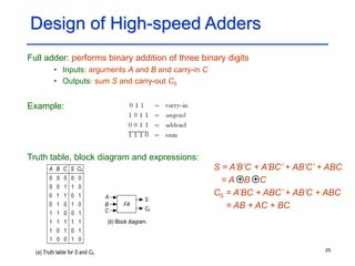
Full adder: performs binary addition of three binary digits
• Inputs: arguments A and B and carry-in C
• Outputs: sum S and carry-out C0
Example:
Truth table, block diagram and expressions:
S
C
(a) Truth table for S and C0.
C0
A B
FA
C
S
C0
0 0 0 0
0
B
A
0 0 1 0
1
1 1 0 1
0
1 1 1 1
1
1 0 1 1
0
1 0 0 0
1
0 1 0 0
1
0 1 1 1
0
(b) Block diagram.
S = A’B’C + A’BC’ + AB’C’ + ABC
= A B C
C0 = A’BC + ABC’ + AB’C + ABC
= AB + AC + BC
+ +
26
Ripple-carry Adder
Ripple-carry adder: Stages of full adders
• Cf: forced carry
• C0(n-1): overflow carry
Si = Ai Bi Ci
C0i = AiBi + AiCi + BiCi
C1
S1
C01
B1
A1
C0(n-1)
FA0
Cf
S0
B0
A0
Cn-1
Bn-1
An-1
Sn-1
FA1
FAn-1
+ +
Time required:
• Time per full adder: 2 units
• Time for ripple-carry adder: 2n units
27
Carry-lookahead Adder
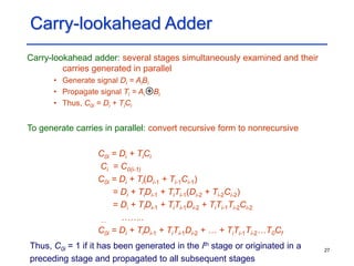
Carry-lookahead adder: several stages simultaneously examined and their
carries generated in parallel
• Generate signal Di = AiBi
• Propagate signal Ti = Ai Bi
• Thus, C0i = Di + TiCi
To generate carries in parallel: convert recursive form to nonrecursive
C0i = Di + TiCi
Ci = C0(i-1)
C0i = Di + Ti(Di-1 + Ti-1Ci-1)
= Di + TiDi-1 + TiTi-1(Di-2 + Ti-2Ci-2)
= Di + TiDi-1 + TiTi-1Di-2 + TiTi-1Ti-2Ci-2
... ……..
C0i = Di + TiDi-1 + TiTi-1Di-2 + … + TiTi-1Ti-2…T0Cf
+
Thus, C0i = 1 if it has been generated in the ith stage or originated in a
preceding stage and propagated to all subsequent stages
28
Carry-lookahead Adder (Contd.)
Implementation of lookahead for the complete adder impractical:
• Divide the n stages into groups
• Full carry lookahead within group
• Ripple carry between groups
Example: Three-digit adder group with full carry lookahead
B
A2
Cg1 = C02
S2
B2
SN2
C2
CN2
(a) Block diagram of initial three-stage group
Cf
A B
A1
C01
S1
B1
SN1
CN1
A B0
A0
C00
S0
B0
SN0
CN0
A0
C1
C00
Cf
T0
D0
(CN0)
C01
(CN1)
T0
T1
Cf
D0
T1
D1
Cf
(CN2)
T1
T2
D0
D1
T2
D2
Cg1 = C02
T1
T2
T0
(b) The carry networks
Di = AiBi
Ti = Ai Bi
+
Time taken:
• 4 time units for Cg1
• Only 2 time units for Cg2 and other
group carries
29
30-bit Adder
Example: divide n stages into groups of three stages
• Time taken: 4 + 2n/3 time units
• 50% additional hardware for a threefold speedup
Bi Ai
Cg10
S29 S27
SN29 SN27
CN29 CN27
Cg9
Bi Ai Cf
S2 S0
SN2 SN0
CN2 CN0
Bi Ai
Cg2
S5 S3
SN5 SN3
CN5 CN3
Cg1
30
Metal-oxide Semiconductor (MOS)
Transistors and Gates
Complementary metal-oxide semiconductor (CMOS): currently the
dominant technology
• Two types of transistors: nMOS and pMOS
x
x
(a) nMOS transistor
x
x
(d) pMOS transistor
(g) Complementary
switch
x = 0
x = 1
(b) nMOS operation
x = 1
x = 0
(e) pMOS operation
x = 0
x = 1
(h) Complementary
switch operation
a b
a
a
a
a
a
a
a
a
b
b
b
b
b
b
b
b
x
a b
(c) nMOS model
x b
(f) pMOS model
a
x
(i) Complementary
switch model
a b
31
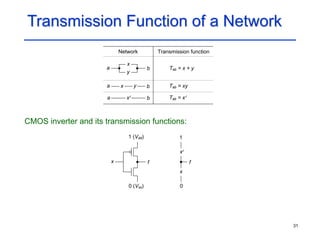
Transmission Function of a Network
CMOS inverter and its transmission functions:
Tab = x + y
a
x
Network
y
a
b
Transmission function
x y b
x
a b Tab = x
Tab = xy
x
1 (Vdd)
x f
x
0 (Vss)
f
1
0
32
CMOS NAND/NOR Gates
x y
1 (Vdd)
x f
0 (Vss)
y
1
x
f
0
y
(a) CMOS NAND gate and its transmission functions.
x
y
1 (Vdd)
x
f
0 (Vss)
y
1
x
f
0
y
(b) CMOS NOR gate and its transmission functions.
33
Analysis of Series-parallel Networks
Algebra of MOS networks: isomorphic to switching algebra
Example: Find the transmission function of the network and its
complementary switch based and complex gate CMOS implementations
(a) Tab = x [(y z + z y)w + w + y + x z ].
b
y
b
z
z
y
z
x
a
w
w
z x
y
w
y
x
a
(b) Tab = x (w + y + z ).
x
w y z
d
c
(c) Tcd = Tab = x + w yz.
Tab
x
x
y
y
z
z
w
w
1
x
1 (Vdd)
x
Tab
w
0 (Vss)
y
w
z
z
y
pMOS network
nMOS network
Complementary
switch based
Complex
gate
34
Analysis of Non-series-parallel Networks
Obtaining the transmission function:
• Tie sets: minimal paths between two terminals
• Cut sets: minimal sets of branches, when open, ensure no transmission
between the two terminals
w
i j
(a) Tie sets. Tij = wx + wvz + yvx + yz.
z
y
v
x
w
i j
(b) Cut sets. Tij = (w + y)(w + v + z)(x + v + y)(x + z).
z
y
v
x
35
Synthesis of MOS Networks
Sneak paths in non-series-parallel networks: undesired paths that may
change the transmission function
• Occur because of bilateral nature of MOS transistors
Example: Design a minimal network with BCD inputs that produces a 1
whenever the input is 3 or a multiple of 3
Sneak path: z’xx’w – OK since it has no effect on the transmission function
y
z
z
w
x
x y
(b) Series-parallel realization of T.
z
z
w
x
x y
(c) Minimal realization of T.
(a) Map for T = wz + xyz + x yz.
1
1
00 01 11 10
00
01
11
10
wx
1
yz
36
Synthesis of MOS Networks (Contd.)
Example: Design a minimal network to realize T(w,x,y,z) = (0,3,13,14,15)

(b) Series-parallel realization of T.
(a) Map for T = wxy + wxz
+ w x y z + w x yz.
1
1
00 01 11 10
00
01
11
10
wx
1
yz
1
1
y
w
w
y
x
x
z
z
z
y
(c) An alternative series-parallel realization of T.
y
w
w
y
x
x
z
y
z
z
(d) A minimum realization of T.
y
w
w y
x
x
y
z
z

3306565.ppt

  • 1.
    Zvi Kohavi andNiraj K. Jha 1 Logical Design
  • 2.
    2 Design with BasicLogic Gates Logic gates: perform logical operations on input signals Positive (negative) logic polarity: constant 1 (0) denotes a high voltage and constant 0 a low (high) voltage Synchronous circuits: driven by a clock that produces a train of equally spaced pulses Asynchronous circuits: are almost free-running and do not depend on a clock; controlled by initiation and completion signals Fanout: number of gate inputs driven by the output of a single gate Fanin: bound on the number of inputs a gate can have Propagation delay: time to propagate a signal through a gate
  • 3.
    3 Analysis of CombinationalCircuits Circuit analysis: determine the Boolean function that describes the circuit • Done by tracing the output of each gate, starting from circuit inputs and continuing towards each circuit output Example: a multi-level realization of a full binary adder (A + B + C)[AB + C(A + B)] AB B AB + (A + B)C A ABC (A + B)C C A + B + C A + B C0 S C0 = AB + (A + B)C = AB + AC + BC S = (A + B + C)[AB + (A + B)C]’ + ABC = (A + B + C)(A’ + B’)(A’ + C’)(B’ + C’) + ABC = AB’C’ + A’BC’ + A’B’C + ABC = A B C + +
  • 4.
    4 Simple Design Problems Parallelparity-bit generator: produces output value 1 if and only if an odd number of its inputs have value 1 P = x’y’z + x’yz’ + xy’z’ + xyz 0 0 1 1 0 1 xy z 0 1 00 01 11 10 1 0 z x y P (a) Map. (b) Implementation.
  • 5.
    5 Simple Design Problems(Contd.) Serial-to-parallel converter: distributes a sequence of binary digits on a serial input to a set of different outputs, as specified by external control signals C1 C2 L1 L4 L3 L2 x
  • 6.
    6 Logic Design withIntegrated Circuits Small scale integration (SSI): integrated circuit packages containing a few gates; e.g., AND, OR, NOT, NAND, NOR, XOR Medium scale integration (MSI): packages containing up to about 100 gates; e.g., code converters, adders Large scale integration (LSI): packages containing thousands of gates; arithmetic unit Very large scale integration (VLSI): packages with millions of gates
  • 7.
    7 Comparators n-bit comparator: comparesthe magnitude of two numbers X and Y, and has three outputs f1, f2, and f3 • f1 = 1 iff X > Y • f2 = 1 iff X = Y • f3 = 1 iff X < Y x1 f1 y2 x2 y1 x1 y1 00 01 11 10 (b) Map for f1, f2, and f3. 00 01 11 10 3 x1x2 y1y2 2 3 3 1 2 3 3 1 1 2 1 1 1 3 2 x1 f3 f2 f1 y2 y1 x2 (a) Block diagram. (c) Circuit for f1. 2-bit comparator f1 = x1x2y2’ + x2y1’y2’ + x1y1’ = (x1 + y1’)x2y2’ + x1y1’ f2 = x1’x2’y1’y2’ + x1’x2y1’y2 + x1x2’y1y2’ + x1x2y1y2 = x1’y1’(x2’y2’ + x2y2) + x1y1(x2’y2’ + x2y2) = (x1’y1’ + x1y1)(x2’y2’ + x2y2) f3 = x2’y1y2 + x1’x2’y2 + x1’y1 = x2’y2(y1 + x1’) + x1’y1
  • 8.
    8 4-bit/12-bit Comparators Four-bit comparator:11 inputs (four for X, four for Y, and three connected to outputs f1, f2 and f3 of the preceding stage) 12-bit comparator: x1 f3 f2 f1 y4 y1 x4 (a) A 4-bit comparator. Inputs from preceding stage x1 f3 f2 f1 y4 y1 x4 y8 y5 y12 y9 x12 x9 x8 x5 > = < > = < > = < > = < > = < > = < > = < > = < (b) A 12-bit comparator. 0 0 1
  • 9.
    9 Data Selectors Multiplexer: electronicswitch that connects one of n inputs to the output Data selector: application of multiplexer • n data input lines, D0, D1, …, Dn-1 • m select digit inputs s0, s1, …, sm-1 • 1 output Enable (a) Block diagram. Select number Data inputs D7 D0 D1 D2 D3 D4 D5 D6 s2 s0 s1 z z z (b) Logic diagram. s0 s1 s2 D0 D1 D2 D3 D4 D5 D6 D7 Enable Select number Data inputs
  • 10.
    10 Implementing Switching Functionswith Data Selectors Data selectors: can implement arbitrary switching functions Example: implementing two-variable functions z s D1 D0 Enable z = sD1 + s D0 If s = A, B = D0, and B = D1, then z = A B. If s = A, D0 = 1, and D1 = B , then z = A + B. +
  • 11.
    11 Implementing Switching Functionswith Data Selectors (Contd.) To implement an n-variable function: a data selector with n-1 select inputs and 2n-1 data inputs Implementing three-variable functions: z = s2’s1’D0 + s2’s1D1 + s2s1’D2 + s2s1D3 Example: s1 = A, s2 = B, D0 = C, D1 = 1, D2 = 0, D3 = C’ z = A’B’C + AB’ + ABC’ = AC’ + B’C General case: Assign n-1 variables to the select inputs and last variable and constants 0 and 1 to the data inputs such that desired function results
  • 12.
    12 Priority Encoders Priority encoder:n input lines and log2n output lines • Input lines represent units that may request service • When inputs pi and pj, such that i > j, request service simultaneously, line pi has priority over line pj • Encoder produces a binary output code indicating which of the input lines requesting service has the highest priority Example: Eight-input, three-output priority encoder z4 = p4p5’p6’p7’ + p5p6’p7’ + p6p7’ + p7 = p4 + p5 + p6 + p7 z2 = p2p3’p4’p5’p6’p7’ + p3p4’p5’p6’p7’ + p6p7’ + p7 = p2p4’p5’ + p3p4’p5’ + p6 + p7 z1 = p1p2’p3’p4’p5’p6’p7’ + p3p4’p5’p6’p7’ + p5p6’p7’ + p7 = p1p2’p4’p6’ + p3p4’p6’ + p5p6’ + p7 Enable z1 p0 z4 z0 (a) Block diagram. Priority encoder z2 p7 p6 p5 p4 p3 p1 p2 z4 p7 (b) Truth table. z2 p6 0 0 0 0 0 0 0 1 0 1 1 0 1 0 1 1 1 1 0 1 1 0 0 0 1 0 0 0 0 1 0 1 0 1 0 Input lines Outputs p5 p4 z1 0 0 0 0 0 0 0 0 0 0 0 0 0 0 0 0 0 0 0 1 1 1 1 1 1 p3 p2 p1 p0
  • 13.
    13 Priority Encoders (Contd.) (c)Logic diagram. z1 Enable z4 z2 p7 p6 p5 p4 p3 p2 p1 p0 z0 Request indicator
  • 14.
    14 Decoders Decoders with ninputs and 2n outputs: for any input combination, only one output is 1 Useful for: • Routing input data to a specified output line, e.g., in addressing memory • Basic building blocks for implementing arbitrary switching functions • Code conversion • Data distribution Example: 2-to-4- decoder x w f0 = w x f3 = wx f2 = wx f1 = w x
  • 15.
    15 Decoders (Contd.) Example: 4-to-16decoder made of two 2-to-4 decoders and a gate- switching matrix x w y f0 z f0 f12 f8 f4 f1 f13 f9 f5 f2 f14 f10 f6 f3 f15 f11 f7 2-to-4 2-to-4 f3 f2 f1 f0 f3 f2 f1
  • 16.
    16 Decimal Decoder BCD-to-decimal: 4-to-16decoder made of two 2-to-4 decoders and a gate- switching matrix Enable f1 w f0 f4 f3 z y x (a) Block diagram. (b) Map. f9 00 01 11 10 00 01 11 10 wx yz Decimal decoder f9 f2 f8 f7 f6 f5 f0 f1 f2 f3 f4 f5 f6 f7 f8 x y f0 f3 f2 f1 (c) Logic diagram. f4 f7 f6 f5 f9 f8 w z Enable
  • 17.
    17 Decimal Decoder (Contd.) Implementationusing a partial-gate matrix: w w x x w x y f3 f7 z y f0 f4 z y f2 f6 z y f1 f5 z f9 f8
  • 18.
    18 Implementing Arbitrary Switching Functions Example:Realize a distinct minterm at each output f15 f1 A f0 f9 f5 D C B 4-to-16 line decoder Enable f = (1,5,9,15)
  • 19.
    19 Demultiplexers Demultiplexers: decoder with1data input and n address inputs • Directs input to any one of the 2n outputs Example: A 4-output demultiplexer Enable 2n outputs n-bit address Data input C1 C2 L1 L4 L3 L2 x
  • 20.
    20 Seven-segment Display Seven-segment display:BCD to seven-segment decoder and seven LEDs Seven-segment pattern and code: D E x1 C A B x4 x3 x2 BCD to 7-segment decoder G F A B C D E F G A = x1 + x2’x4’ + x2x4 + x3x4 B = x2’ + x3’x4’ + x3x4 C = x2 + x3’ + x4 D = x2’x4’ + x2’x3 + x3x4’ + x2x3’x4 E = x2’x4’ + x3x4’ F = x1 + x2x3’ + x2x4’ + x3’x4’ G = x1 + x2’x3 + x2x3’ + x3x4’
  • 21.
    21 Sine Generators Combinational sinegenerators: for fast and repeated evaluation of sine • Input: angle in radians converted to binary • Output: sine in binary z1 = x1’x2 + x1x2’ + x2x3’ + x1’x3x4 z2 = x1x2’ + x3x4’ + x1’x2x4 z3 = x3x4’ + x2x3 + x2x4’ + x2’x3’x4 + x1x4’ z4 = x2’x3’x4 + x2x3’x4’ + x1x2’x3’ + x1x3x4 + x1’x2x4 z1 x4 (a) Truth table. z2 x3 0 0 0 0 0 0 0 1 0 1 1 1 0 1 0 1 1 1 1 1 1 0 1 1 0 1 0 0 0 1 0 1 0 0 1 0 1 1 1 0 Angle x sin( x) x2 x1 z4 z3 0 0 0 0 0 0 0 0 0 0 0 0 0 0 0 0 0 0 0 0 0 0 1 1 1 1 1 1 1 1 1 1 0 0 0 0 1 1 1 1 1 1 1 1 1 1 1 1 1 1 1 1 1 1 1 1 1 1 1 1 1 1 1 1 1 1 1 1 1 1 1 1 1 1 1 1 1 1 0 0 0 0 0 0 0 0 0 0 Sine generator x3 z1 x2 x1 (b) Block diagram. x4 z4 z3 z2 sin( x)
  • 22.
    22 NAND/NOR Circuits Switching algebra:not directly applicable to NAND/NOR logic NAND and NOR gate symbols A A A (AB) B B (A + B) (a) A B A + B A B B (d) (b) (c)
  • 23.
    23 Analysis of NAND/NORNetworks Example: circles (inversions) at both ends of a line cancel each other B + C A (EF ) D + EF [(B + C )(D + EF )] (a) NAND-logic circuit. F E D T = A + (B + C )(D + EF ) B C 5 4 2 B + C A EF D + EF (B + C )(D + EF ) (b) Logically equivalent AND-OR circuit. F E D T = A + (B + C )(D + EF ) B C 1 3
  • 24.
    24 Synthesis of NAND/NORNetworks Example: Realize T = w(y+z) + xy’z’ y y z [w(y + z)] y + z (a) First realization. (xy z ) w x z T = w(y + z) + xy z 1 2 3 4 y y z [w(y + z)] y + z (b) Realization with two-input gates. y z w x z T = w(y + z) + xy z 1 2 3 4 (y z ) 3 (xy z )
  • 25.
    25 Design of High-speedAdders Full adder: performs binary addition of three binary digits • Inputs: arguments A and B and carry-in C • Outputs: sum S and carry-out C0 Example: Truth table, block diagram and expressions: S C (a) Truth table for S and C0. C0 A B FA C S C0 0 0 0 0 0 B A 0 0 1 0 1 1 1 0 1 0 1 1 1 1 1 1 0 1 1 0 1 0 0 0 1 0 1 0 0 1 0 1 1 1 0 (b) Block diagram. S = A’B’C + A’BC’ + AB’C’ + ABC = A B C C0 = A’BC + ABC’ + AB’C + ABC = AB + AC + BC + +
  • 26.
    26 Ripple-carry Adder Ripple-carry adder:Stages of full adders • Cf: forced carry • C0(n-1): overflow carry Si = Ai Bi Ci C0i = AiBi + AiCi + BiCi C1 S1 C01 B1 A1 C0(n-1) FA0 Cf S0 B0 A0 Cn-1 Bn-1 An-1 Sn-1 FA1 FAn-1 + + Time required: • Time per full adder: 2 units • Time for ripple-carry adder: 2n units
  • 27.
    27 Carry-lookahead Adder Carry-lookahead adder:several stages simultaneously examined and their carries generated in parallel • Generate signal Di = AiBi • Propagate signal Ti = Ai Bi • Thus, C0i = Di + TiCi To generate carries in parallel: convert recursive form to nonrecursive C0i = Di + TiCi Ci = C0(i-1) C0i = Di + Ti(Di-1 + Ti-1Ci-1) = Di + TiDi-1 + TiTi-1(Di-2 + Ti-2Ci-2) = Di + TiDi-1 + TiTi-1Di-2 + TiTi-1Ti-2Ci-2 ... …….. C0i = Di + TiDi-1 + TiTi-1Di-2 + … + TiTi-1Ti-2…T0Cf + Thus, C0i = 1 if it has been generated in the ith stage or originated in a preceding stage and propagated to all subsequent stages
  • 28.
    28 Carry-lookahead Adder (Contd.) Implementationof lookahead for the complete adder impractical: • Divide the n stages into groups • Full carry lookahead within group • Ripple carry between groups Example: Three-digit adder group with full carry lookahead B A2 Cg1 = C02 S2 B2 SN2 C2 CN2 (a) Block diagram of initial three-stage group Cf A B A1 C01 S1 B1 SN1 CN1 A B0 A0 C00 S0 B0 SN0 CN0 A0 C1 C00 Cf T0 D0 (CN0) C01 (CN1) T0 T1 Cf D0 T1 D1 Cf (CN2) T1 T2 D0 D1 T2 D2 Cg1 = C02 T1 T2 T0 (b) The carry networks Di = AiBi Ti = Ai Bi + Time taken: • 4 time units for Cg1 • Only 2 time units for Cg2 and other group carries
  • 29.
    29 30-bit Adder Example: dividen stages into groups of three stages • Time taken: 4 + 2n/3 time units • 50% additional hardware for a threefold speedup Bi Ai Cg10 S29 S27 SN29 SN27 CN29 CN27 Cg9 Bi Ai Cf S2 S0 SN2 SN0 CN2 CN0 Bi Ai Cg2 S5 S3 SN5 SN3 CN5 CN3 Cg1
  • 30.
    30 Metal-oxide Semiconductor (MOS) Transistorsand Gates Complementary metal-oxide semiconductor (CMOS): currently the dominant technology • Two types of transistors: nMOS and pMOS x x (a) nMOS transistor x x (d) pMOS transistor (g) Complementary switch x = 0 x = 1 (b) nMOS operation x = 1 x = 0 (e) pMOS operation x = 0 x = 1 (h) Complementary switch operation a b a a a a a a a a b b b b b b b b x a b (c) nMOS model x b (f) pMOS model a x (i) Complementary switch model a b
  • 31.
    31 Transmission Function ofa Network CMOS inverter and its transmission functions: Tab = x + y a x Network y a b Transmission function x y b x a b Tab = x Tab = xy x 1 (Vdd) x f x 0 (Vss) f 1 0
  • 32.
    32 CMOS NAND/NOR Gates xy 1 (Vdd) x f 0 (Vss) y 1 x f 0 y (a) CMOS NAND gate and its transmission functions. x y 1 (Vdd) x f 0 (Vss) y 1 x f 0 y (b) CMOS NOR gate and its transmission functions.
  • 33.
    33 Analysis of Series-parallelNetworks Algebra of MOS networks: isomorphic to switching algebra Example: Find the transmission function of the network and its complementary switch based and complex gate CMOS implementations (a) Tab = x [(y z + z y)w + w + y + x z ]. b y b z z y z x a w w z x y w y x a (b) Tab = x (w + y + z ). x w y z d c (c) Tcd = Tab = x + w yz. Tab x x y y z z w w 1 x 1 (Vdd) x Tab w 0 (Vss) y w z z y pMOS network nMOS network Complementary switch based Complex gate
  • 34.
    34 Analysis of Non-series-parallelNetworks Obtaining the transmission function: • Tie sets: minimal paths between two terminals • Cut sets: minimal sets of branches, when open, ensure no transmission between the two terminals w i j (a) Tie sets. Tij = wx + wvz + yvx + yz. z y v x w i j (b) Cut sets. Tij = (w + y)(w + v + z)(x + v + y)(x + z). z y v x
  • 35.
    35 Synthesis of MOSNetworks Sneak paths in non-series-parallel networks: undesired paths that may change the transmission function • Occur because of bilateral nature of MOS transistors Example: Design a minimal network with BCD inputs that produces a 1 whenever the input is 3 or a multiple of 3 Sneak path: z’xx’w – OK since it has no effect on the transmission function y z z w x x y (b) Series-parallel realization of T. z z w x x y (c) Minimal realization of T. (a) Map for T = wz + xyz + x yz. 1 1 00 01 11 10 00 01 11 10 wx 1 yz
  • 36.
    36 Synthesis of MOSNetworks (Contd.) Example: Design a minimal network to realize T(w,x,y,z) = (0,3,13,14,15)  (b) Series-parallel realization of T. (a) Map for T = wxy + wxz + w x y z + w x yz. 1 1 00 01 11 10 00 01 11 10 wx 1 yz 1 1 y w w y x x z z z y (c) An alternative series-parallel realization of T. y w w y x x z y z z (d) A minimum realization of T. y w w y x x y z z