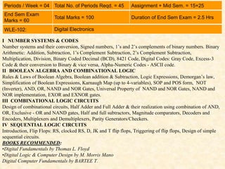
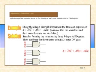
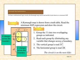
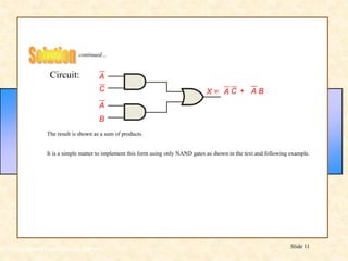
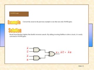
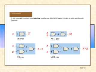
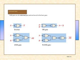
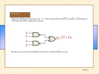
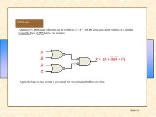
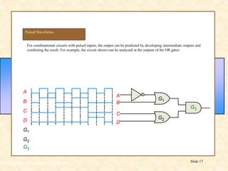
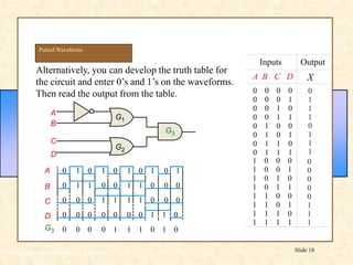
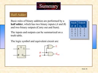
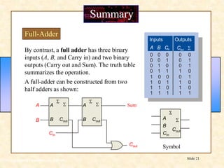
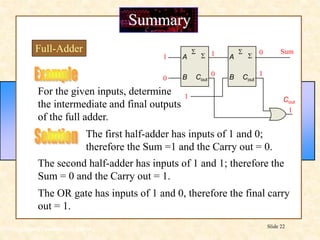
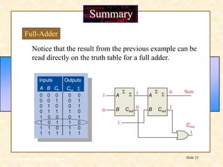
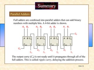
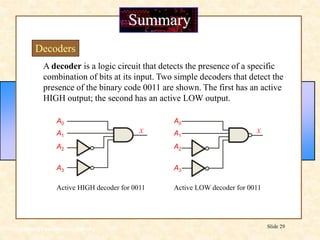
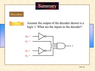
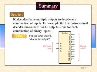
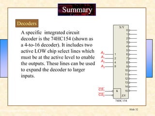
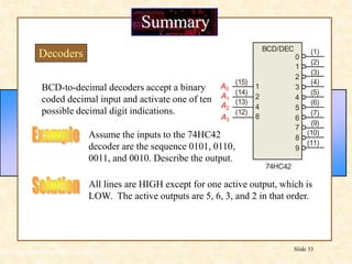
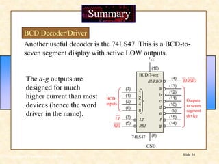
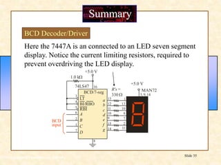
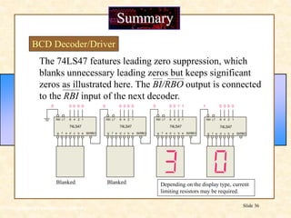
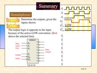
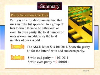
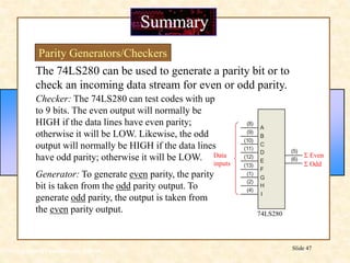
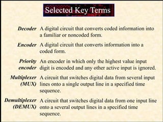
SlideShare a Scribd company logo
1 of 49
DIGITAL ELECTRONICS (WLE-102)
UNIT-III: COMBINATIONAL LOGIC
CIRCUITS
Presented by:
Shahnawaz Uddin
Periods / Week = 04 Total No. of Periods Reqd. = 45 Assignment + Mid Sem. = 15+25
End Sem Exam
Marks = 60
Total Marks = 100 Duration of End Sem Exam = 2.5 Hrs
WLE-102: Digital Electronics
I NUMBER SYSTEMS & CODES
Number systems and their conversion, Signed numbers, 1’s and 2’s complements of binary numbers. Binary
Arithmetic: Addition, Subtraction, 1’s Complement Subtraction, 2’s Complement Subtraction,
Multiplication, Division, Binary Coded Decimal (BCD), 8421 Code, Digital Codes: Gray Code, Excess-3
Code & their conversion to Binary & vice versa, Alpha-Numeric Codes - ASCII code.
II BOOLEAN ALGEBRA AND COMBINATIONAL LOGIC
Rules & Laws of Boolean Algebra, Boolean addition & Subtraction, Logic Expressions, Demorgan’s law,
Simplification of Boolean Expressions, Karnaugh Map (up to 4-variables), SOP and POS form, NOT
(Inverter), AND, OR, NAND and NOR Gates, Universal Property of NAND and NOR Gates, NAND and
NOR implementation, EXOR and EXNOR gates.
III COMBINATIONAL LOGIC CIRCUITS
Design of combinational circuits, Half Adder and Full Adder & their realization using combination of AND,
OR, Exclusive - OR and NAND gates, Half and full subtractors, Magnitude comparators, Decoders and
Encoders, Multiplexers and Demultiplexers, Parity Generators/Checkers.
IV SEQUENTIAL LOGIC CIRCUITS
Introduction, Flip Flops: RS, clocked RS, D, JK and T flip flops, Triggering of flip flops, Design of simple
sequential circuits.
BOOKS RECOMMENDED:
•Digital Fundamentals by Thomas L. Floyd
•Digital Logic & Computer Design by M. Morris Mano
Digital Computer Fundamentals by BARTEE T.
Floyd, Digital Fundamentals, 10th ed
Slide 3
In Sum-of-Products (SOP) form, basic combinational circuits can be directly implemented with AND-OR combinations if
the necessary complement terms are available.
Combinational Logic Circuits
JK
J
K
A
B
AB
Product terms
Sum-of-products
Product term
C
D
CD
AB + CD + + JK
. . .
Floyd, Digital Fundamentals, 10th ed
Slide 4
An example of an SOP implementation is shown. The SOP expression is an AND-OR combination of the input variables
and the appropriate complements.
Combinational Logic Circuits
SOP
DE
ABC
A
B
C
E
D
X = ABC + DE
Floyd, Digital Fundamentals, 10th ed
Slide 5
When the output of a SOP form is inverted, the circuit is called an AND-OR-Invert circuit. The AOI configuration lends
itself to product-of-sums (POS) implementation.
An example of an AOI implementation is shown. The output expression can be changed to a POS expression by applying
DeMorgan’s theorem twice.
Combinational Logic Circuits
POS
DE
ABC
A
B
C
E
D
X = ABC + DE X = ABC + DE
X = (A + B + C)(D + E)
X = (ABC)(DE)
AOI
DeMorgan
Floyd, Digital Fundamentals, 10th ed
Slide 6
The truth table for an exclusive-OR gate is
Exclusive-OR Logic
A
B
Output
Inputs
A B X
0
0
1
1
0
1
0
1
0
1
1
0
Notice that the output is HIGH whenever A and B disagree.
The Boolean expression is
The circuit can be drawn as
X = 1
Symbols:
Distinctive shape Rectangular outline
X = AB + AB
Floyd, Digital Fundamentals, 10th ed
Slide 7
The truth table for an exclusive-NOR gate is
Exclusive-NOR Logic
A
B
Notice that the output is HIGH whenever A and B agree.
The Boolean expression is
The circuit can be drawn as
X
Symbols:
Distinctive shape Rectangular outline
Output
Inputs
A B X
0
0
1
1
0
1
0
1
1
0
0
1
= 1
X = AB + AB
Floyd, Digital Fundamentals, 10th ed
Slide 8
For each circuit, determine if the LED should be on or off.
+5.0 V
+5.0 V
330 W
LED
B
A
+5.0 V
+5.0 V
330 W
LED
B
A
+5.0 V
+5.0 V
330 W
LED
B
A
(a) (b) (c)
Circuit (a): XOR, inputs agree, output is LOW, LED is ON.
Circuit (b): XNOR, inputs disagree, output is LOW, LED is ON.
Circuit (c): XOR, inputs disagree, output is HIGH, LED is OFF.
Floyd, Digital Fundamentals, 10th ed
Slide 9
Implementing a SOP expression is done by first forming the AND terms; then the terms are ORed together.
Implementing Combinational Logic
Show the circuit that will implement the Boolean expression
X = ABC + ABD + BDE. (Assume that the variables and
their complements are available.)
C
A
B
E
D
B
A
B
D
Start by forming the terms using three 3-input AND gates.
Then combine the three terms using a 3-input OR gate.
X = ABC + ABD + BDE
Floyd, Digital Fundamentals, 10th ed
Slide 10
For basic combinational logic circuits, the Karnaugh map can be read and the circuit drawn as a minimum SOP.
Karnaugh Map Implementation
A Karnaugh map is drawn from a truth table. Read the
minimum SOP expression and draw the circuit.
1. Group the 1’s into two overlapping
groups as indicated.
2. Read each group by eliminating any
variable that changes across a boundary.
C C
AB
AB
AB
AB
1
1 1
C C
AB
AB
AB
AB
1
1 1
B changes
across this
boundary
C changes
across this
boundary
3. The vertical group is read AC.
4. The horizontal group is read AB.
The circuit is on the next slide:
Floyd, Digital Fundamentals, 10th ed
Slide 11
Circuit:
C
A
A
C
A + A B
continued…
X =
The result is shown as a sum of products.
It is a simple matter to implement this form using only NAND gates as shown in the text and following example.
B
Floyd, Digital Fundamentals, 10th ed
Slide 12
NAND Logic
Convert the circuit in the previous example to one that uses only NAND gates.
Recall from Boolean algebra that double inversion cancels. By adding inverting bubbles to above circuit, it is easily
converted to NAND gates:
C
A
B
A
C
A + A B
X =
Floyd, Digital Fundamentals, 10th ed
Slide 13
NAND gates are sometimes called universal gates because they can be used to produce the other basic Boolean
functions.
Universal Gates
Inverter
A
A
AND gate
A
B
AB
A
B
A + B
OR gate
A
B
A + B
NOR gate
Floyd, Digital Fundamentals, 10th ed
Slide 14
NOR gates are also universal gates and can form all of the basic gates.
Universal Gates
Inverter
A
A
OR gate
A
B
A + B
A
B
AB
AND gate
A
B
AB
NAND gate
Floyd, Digital Fundamentals, 10th ed
Slide 15
Recall from DeMorgan’s theorem that AB = A + B. By using equivalent symbols, it is simpler to read the logic of
SOP forms. The earlier example shows the idea:
NAND Logic
C
A
B
A
C
A + A B
X =
The logic is easy to read if you (mentally) cancel the two connected bubbles on a line.
Floyd, Digital Fundamentals, 10th ed
Slide 16
NOR Logic
B
A
C
A
X =
Again, the logic is easy to read if you cancel the two connected bubbles on a line.
Alternatively, DeMorgan’s theorem can be written as A + B = A B. By using equivalent symbols, it is simpler
to read the logic of POS forms. For example,
(A + B)(A + C)
Floyd, Digital Fundamentals, 10th ed
Slide 17
Pulsed Waveforms
For combinational circuits with pulsed inputs, the output can be predicted by developing intermediate outputs and
combining the result. For example, the circuit shown can be analyzed at the outputs of the OR gates:
A
B
C
D
A
B
C
D
G1
G2
G3
G1
G2
G3
Floyd, Digital Fundamentals, 10th ed
Slide 18
Pulsed Waveforms
Alternatively, you can develop the truth table for
the circuit and enter 0’s and 1’s on the waveforms.
Then read the output from the table.
A
B
C
D
A
B
C
D
G1
G2
G3
G3
Inputs
A B C D
Output
0 0 0 0
0 0 0 1
0 0 1 0
0 0 1 1
0 1 0 0
0 1 0 1
0 1 1 0
0 1 1 1
1 0 0 0
1 0 0 1
1 0 1 0
1 0 1 1
1 1 0 0
1 1 0 1
1 1 1 0
1 1 1 1
0 1 0 1 0 1 0 1 0 1
0 1 1 0 0 1 1 0 0 0
0 0 0 1 1 1 1 0 0 0
0 0 0 0 0 0 0 1 1 0
0 0 0 0 1 1 1 0 1 0
X
0
1
1
1
0
1
1
1
0
0
0
0
0
1
1
1
Universal gate
Negative-OR
Negative-AND
Either a NAND or a NOR gate. The term universal refers to a property of a gate that permits any logic
function to be implemented by that gate or by a combination of gates of that kind.
The dual operation of a NAND gate when the inputs are active-LOW.
The dual operation of a NOR gate when the inputs are active-LOW.
Floyd, Digital Fundamentals, 10th ed
Slide 20
Basic rules of binary addition are performed by a
half adder, which has two binary inputs (A and B)
and two binary outputs (Carry out and Sum).
Summary
Half-Adder
The inputs and outputs can be summarized on a
truth table.
Outputs
Inputs
A B Cout S
0
0
1
1
0
1
0
1
0 0
0 1
0 1
1 0
A
B
S
Cout
The logic symbol and equivalent circuit are:
A
B
S
Cout
S
Floyd, Digital Fundamentals, 10th ed
Slide 21
Summary
Full-Adder
By contrast, a full adder has three binary
inputs (A, B, and Carry in) and two binary
outputs (Carry out and Sum). The truth table
summarizes the operation.
Outputs
Inputs
A B Cout S
Cin
0
1
0
1
0
1
0
1
0
0
0
0
0
0
1
1
1
1
0
0
1
1
1
1
0
0
0
1
0
1
1
0
0
1
1
0
1
1
0
1
A full-adder can be constructed from two
half adders as shown:
A
B
S
Cout
S A
B
S
Cout
S
A
B
Sum
Cout
Cin
A
B
S
Cout
S
Cin
Symbol
Floyd, Digital Fundamentals, 10th ed
Slide 22
Summary
Full-Adder
A
B
S
Cout
S A
B
S
Cout
S
For the given inputs, determine
the intermediate and final outputs
of the full adder.
1
1
0
1
0
The first half-adder has inputs of 1 and 0;
therefore the Sum =1 and the Carry out = 0.
The second half-adder has inputs of 1 and 1; therefore the
Sum = 0 and the Carry out = 1.
The OR gate has inputs of 1 and 0, therefore the final carry
out = 1.
1
0
1
Sum
Cout
Floyd, Digital Fundamentals, 10th ed
Slide 23
Summary
Full-Adder
Outputs
Inputs
A B Cout S
Cin
0
1
0
1
0
1
0
1
0
0
0
0
0
0
1
1
1
1
0
0
1
1
1
1
0
0
0
1
0
1
1
0
0
1
1
0
1
1
0
1
A
B
S
Cout
S A
B
S
Cout
S
1
1
0
1
0 1
0
1
Sum
Cout
Notice that the result from the previous example can be
read directly on the truth table for a full adder.
Floyd, Digital Fundamentals, 10th ed
Slide 24
Summary
Parallel Adders
Full adders are combined into parallel adders that can add binary
numbers with multiple bits. A 4-bit adder is shown.
A B
S
Cout
Cin A B
S
Cout
Cin A B
S
Cout
Cin A B
S
Cout
Cin
A1 B1
S1
C0
S2
S3
S4
C1
C2
C3
C4
A2 B2
A3 B3
A4 B4
The output carry (C4) is not ready until it propagates through all of the
full adders. This is called ripple carry, delaying the addition process.
Floyd, Digital Fundamentals, 10th ed
Slide 25
Summary
Parallel Adders
The logic symbol for a 4-bit parallel adder is shown. This 4-bit adder
includes a carry in (labeled (C0) and a Carry out (labeled C4).
The 74LS283 is an example. It features look-ahead carry, which adds
logic to minimize the output carry delay. For the 74LS283, the
maximum delay to the output carry is 17 ns.
Binary
number A
Binary
number B
Input
carry
4-bit
sum
Output
carry
1
2
3
4
1
2
3
4
1
2
3
4
C0 C4
S
Floyd, Digital Fundamentals, 10th ed
Slide 26
Summary
Comparators
The function of a comparator is to compare the magnitudes of two
binary numbers to determine the relationship between them. In the
simplest form, a comparator can test for equality using XNOR gates.
How could you test two 4-bit numbers for equality?
AND the outputs of four XNOR gates.
A1
B1
A2
B2
A3
B3
A4
B4
Output
Floyd, Digital Fundamentals, 10th ed
Slide 27
Summary
Comparators
IC comparators provide outputs to indicate which of the numbers is
larger or if they are equal. The bits are numbered starting at 0, rather
than 1 as in the case of adders. Cascading inputs are provided to
expand the comparator to larger numbers.
Outputs
A1
A0
A2
A3
B1
B0
B2
B3
Cascading
inputs
COMP
A = B
A < B
A > B
A = B
A < B
A > B
0
0
3
3
A
A
The IC shown is the
4-bit 74LS85.
Floyd, Digital Fundamentals, 10th ed
Slide 28
Summary
Comparators
IC comparators can be expanded using the cascading inputs as shown.
The lowest order comparator has a HIGH on the A = B input.
Outputs
A1
A0
A2
A3
B1
B0
B2
B3
COMP
A = B
A < B
A > B
A = B
A < B
A > B
0
0
3
3
A
A
A5
A4
A6
A7
B5
B4
B6
B7
+5.0 V
COMP
A = B
A < B
A > B
A = B
A < B
A > B
0
0
3
3
A
A
LSBs MSBs
Floyd, Digital Fundamentals, 10th ed
Slide 29
Summary
Decoders
A decoder is a logic circuit that detects the presence of a specific
combination of bits at its input. Two simple decoders that detect the
presence of the binary code 0011 are shown. The first has an active
HIGH output; the second has an active LOW output.
A1
A0
A2
A3
X
Active HIGH decoder for 0011
A1
A0
A2
A3
X
Active LOW decoder for 0011
Floyd, Digital Fundamentals, 10th ed
Slide 30
Summary
Decoders
A0 = 0
A1 = 1
A2 = 0
A3 = 1
1
Assume the output of the decoder shown is a
logic 1. What are the inputs to the decoder?
Floyd, Digital Fundamentals, 10th ed
Slide 31
Summary
Decoders
IC decoders have multiple outputs to decode any
combination of inputs. For example the binary-to-decimal
decoder shown here has 16 outputs – one for each
combination of binary inputs.
Bin/Dec
A0
0
1
2
3
4
5
6
7
8
9
10
11
12
13
14
15
4-bit binary
input
Decimal
outputs
A1
A2
A3
1
1
0
1
1
1
1
1
1
1
1
1
1
1
0
1
1
1
1
1
For the input shown,
what is the output?
Floyd, Digital Fundamentals, 10th ed
Slide 32
Summary
Decoders
A specific integrated circuit
decoder is the 74HC154 (shown as
a 4-to-16 decoder). It includes two
active LOW chip select lines which
must be at the active level to enable
the outputs. These lines can be used
to expand the decoder to larger
inputs.
CS2
A1
A0
A2
A3
15
12
13
14
1
2
3
4
9
10
11
5
6
7
8
0
&
4
8
1
2
CS1
X/Y
EN
74HC154
Floyd, Digital Fundamentals, 10th ed
Slide 33
Summary
Decoders
BCD-to-decimal decoders accept a binary
coded decimal input and activate one of ten
possible decimal digit indications.
BCD/DEC
0
1
2
3
4
5
6
7
8
9
1
2
4
8
74HC42
(11)
(10)
(9)
(7)
(6)
(5)
(4)
(3)
(2)
(1)
(15)
(14)
(13)
(12)
A1
A0
A2
A3
Assume the inputs to the 74HC42
decoder are the sequence 0101, 0110,
0011, and 0010. Describe the output.
All lines are HIGH except for one active output, which is
LOW. The active outputs are 5, 6, 3, and 2 in that order.
Floyd, Digital Fundamentals, 10th ed
Slide 34
Summary
BCD Decoder/Driver
Another useful decoder is the 74LS47. This is a BCD-to-
seven segment display with active LOW outputs.
The a-g outputs are
designed for much
higher current than most
devices (hence the word
driver in the name).
a
b
c
d
e
f
g
1
2
4
8
(16)
(4)
(13)
(12)
(11)
(10)
(9)
(15)
(14)
(1)
(2)
(6)
(7)
(3)
(5)
(8)
BCD
inputs
Outputs
to seven
segment
device
GND
VCC
BCD/7-seg
BI/RBO BI/RBO
LT
RBI
LT
RBI
74LS47
Floyd, Digital Fundamentals, 10th ed
Slide 35
Summary
BCD Decoder/Driver
Here the 7447A is an connected to an LED seven segment
display. Notice the current limiting resistors, required to
prevent overdriving the LED display.
VCC
GND
+5.0 V
+5.0 V
R's =
330 W
a
b
c
d
e
f
g
a
b
c
d
e
f
g
MAN72
74LS47
LT
BI/RBO
RBI
1.0 kW
1
1 2
2
3,9,14
3
4
5
6
7
7
8
8
9
10
10
11
11
12 13
13
14
15
16
BCD/7-seg
BCD
input
D
C
B
A
Floyd, Digital Fundamentals, 10th ed
Slide 36
Summary
BCD Decoder/Driver
a
b
c
d
e
f
g BI/RBO
0 0 0 0
8 4 2 1
RBI LT
0
74LS47
a
b
c
d
e
f
g BI/RBO
0 0 0 0
8 4 2 1
RBI LT
0
74LS47
a
b
c
d
e
f
g BI/RBO
0 0 1 1
8 4 2 1
RBI LT
0
74LS47
a
b
c
d
e
f
g BI/RBO
0 0 0 0
8 4 2 1
RBI LT
1
74LS47
Blanked Blanked
The 74LS47 features leading zero suppression, which
blanks unnecessary leading zeros but keeps significant
zeros as illustrated here. The BI/RBO output is connected
to the RBI input of the next decoder.
Depending on the display type, current
limiting resistors may be required.
Floyd, Digital Fundamentals, 10th ed
Slide 37
Summary
BCD Decoder/Driver
Blanked Blanked
a
b
c
d
e
f
g BI/RBO
0 1 0 1
8 4 2 1
RBI LT
74LS47
1
a
b
c
d
e
f
g BI/RBO
0 1 1 1
8 4 2 1
RBI LT
74LS47
a
b
c
d
e
f
g BI/RBO
0 0 0 0
8 4 2 1
RBI LT
74LS47
0
a
b
c
d
e
f
g BI/RBO
0 0 0 0
8 4 2 1
RBI LT
74LS47
0
Decimal
point
Trailing zero suppression blanks unnecessary trailing
zeros to the right of the decimal point as illustrated here.
The RBI input is connected to the BI/RBO output of the
following decoder.
Floyd, Digital Fundamentals, 10th ed
Slide 38
Summary
Encoders
An encoder accepts an active logic level on one of its
inputs and converts it to a coded output, such as BCD or
binary.
The decimal to BCD is an encoder
with an input for each of the ten
decimal digits and four outputs that
represent the BCD code for the active
digit. The basic logic diagram is
shown. There is no zero input
because the outputs are all LOW
when the input is zero.
A1
A0
A2
A3
1
2
3
4
5
6
7
8
9
Floyd, Digital Fundamentals, 10th ed
Slide 39
Summary
Encoders
A1
A0
A2
A3
Show how the decimal-to-BCD encoder converts the
decimal number 3 into a BCD 0011.
The top two OR gates have ones as indicated with
the red lines. Thus the output is 0111.
1
2
3
4
5
6
7
8
9
0
0
0
0
0
0
0
0
1
0
0
1
1
Floyd, Digital Fundamentals, 10th ed
Slide 40
Summary
Encoders
The 74HC147 is an example of an IC encoder. It is has ten
active-LOW inputs and converts the active input to an
active-LOW BCD output.
This device is offers additional
flexibility in that it is a priority
encoder. This means that if more
than one input is active, the one
with the highest order decimal
digit will be active.
Decimal
input
BCD
output
1
2
4
8
(16)
(11)
(12)
(13)
(1)
(2)
(4)
(3)
(5)
(9)
(7)
(6)
(14)
(8)
1
2
3
4
5
6
7
8
(10) 9
GND
VCC
HPRI/BCD
74HC147
The next slide shows an application …
Floyd, Digital Fundamentals, 10th ed
Slide 41
Summary
Encoders
VCC
BCD complement of
key press
1
2
3
4
5
6
7
8
9
1
2
4
8
9
8
7
6
5
3
2
1
0
4
R7 R8 R9
R4 R5 R6
R1 R2 R3
R0
Keyboard
encoder HPRI/BCD
74HC147
The zero line is not needed by the
encoder, but may be used by other
circuits to detect a key press.
Floyd, Digital Fundamentals, 10th ed
Slide 42
Summary
Code converters
There are various code converters that change one code to
another. Two examples are the four bit binary-to-Gray
converter and the Gray-to-binary converter.
Show the conversion of binary 0111 to Gray and back.
0
0
0
1
1
1
Binary-to-Gray Gray-to-Binary
MSB
LSB
MSB
LSB
1
0
0
0
1
0
0
1
1
1
Floyd, Digital Fundamentals, 10th ed
Slide 43
MUX
1
2
0
3
1
0
A multiplexer (MUX) selects one data line from two or
more input lines and routes data from the selected line to
the output. The particular data line that is selected is
determined by the select inputs.
Summary
Multiplexers
Two select lines are shown
here to choose any of the
four data inputs.
Data
select
Data
inputs
Data
output
D1
D0
D2
D3
S1
S0
Which data line is selected if
S1S0 = 10? D2
1
0
Floyd, Digital Fundamentals, 10th ed
Slide 44
A demultiplexer (DEMUX) performs the opposite function
from a MUX. It switches data from one input line to two or
more data lines depending on the select inputs.
The 74LS138 was introduced
previously as a decoder but can also
serve as a DEMUX. When
connected as a DEMUX, data is
applied to one of the enable inputs,
and routed to the selected output
line depending on the select
variables. Note that the outputs are
active-LOW as illustrated in the
following example…
Summary
Demultiplexers
74LS138
Y1
Y2
Y3
Y4
Y5
Y6
Y7
Y0
DEMUX
A
A
A
0
1
2
G
G
G
1
2A
2B
Data
select
lines
Enable
inputs
Data
outputs
Floyd, Digital Fundamentals, 10th ed
Slide 45
Determine the outputs, given the
inputs shown.
Summary
Demultiplexers
74LS138
Y1
Y2
Y3
Y4
Y5
Y6
Y7
Y0
DEMUX
A
A
A
0
1
2
G
G
G
1
2A
2B
Data
select
lines
Enable
inputs
Data
outputs
A0
Y0
Y1
Y2
Y3
Y4
Y5
Y6
Y7
A1
A2
G1
G2A
G2B
LOW
LOW
The output logic is opposite to the input
because of the active-LOW convention. (Red
shows the selected line).
Floyd, Digital Fundamentals, 10th ed
Slide 46
Summary
Parity Generators/Checkers
Parity is an error detection method that
uses an extra bit appended to a group of
bits to force them to be either odd or
even. In even parity, the total number of
ones is even; in odd parity the total
number of ones is odd.
11010011
S with odd parity =
S with even parity = 01010011
The ASCII letter S is 1010011. Show the parity
bit for the letter S with odd and even parity.
Floyd, Digital Fundamentals, 10th ed
Slide 47
Summary
Parity Generators/Checkers
The 74LS280 can be used to generate a parity bit or to
check an incoming data stream for even or odd parity.
Checker: The 74LS280 can test codes with up
to 9 bits. The even output will normally be
HIGH if the data lines have even parity;
otherwise it will be LOW. Likewise, the odd
output will normally be HIGH if the data lines
have odd parity; otherwise it will be LOW.
Generator: To generate even parity, the parity
bit is taken from the odd parity output. To
generate odd parity, the output is taken from
the even parity output.
(5)
(6)
(13)
(1)
(11)
(12)
(2)
(10)
(9)
(8)
F
G
D
E
H
C
B
A
(4)
I
74LS280
Data
inputs
S Even
S Odd
Selected Key Terms
Full-adder
Cascading
Ripple carry
Look-ahead
carry
A digital circuit that adds two bits and an input
carry bit to produce a sum and an output carry.
Connecting two or more similar devices in a
manner that expands the capability of one device.
A method of binary addition in which the output
carry from each adder becomes the input carry of
the next higher order adder.
A method of binary addition whereby carries from
the preceding adder stages are anticipated, thus
eliminating carry propagation delays.
Selected Key Terms
Decoder
Encoder
Priority
encoder
Multiplexer
(MUX)
Demultiplexer
(DEMUX)
A digital circuit that converts coded information into
a familiar or noncoded form.
A digital circuit that converts information into a
coded form.
An encoder in which only the highest value input
digit is encoded and any other active input is ignored.
A circuit that switches digital data from several input
lines onto a single output line in a specified time
sequence.
A circuit that switches digital data from one input line
onto a several output lines in a specified time
sequence.

More Related Content

Similar to Digital Electronics Combinational Logic Circuits

Digital Logic Design
Digital Logic Design Digital Logic Design
Digital Logic Design Alihyderkolachi
 
Basic gates and boolean algebra
Basic gates and boolean algebraBasic gates and boolean algebra
Basic gates and boolean algebraSudheesh S Madhav
 
B sc ii sem unit 2(b) ba
B sc ii sem unit 2(b) baB sc ii sem unit 2(b) ba
B sc ii sem unit 2(b) baMahiboobAliMulla
 
Digital Logic Design
Digital Logic Design  Digital Logic Design
Digital Logic Design Alihyderkolachi
 
Chapter 2
Chapter 2Chapter 2
Chapter 2EasyStudy3
 
B sc3 unit 3 boolean algebra
B sc3 unit 3 boolean algebraB sc3 unit 3 boolean algebra
B sc3 unit 3 boolean algebraMahiboobAliMulla
 
Modern+digital+electronics rp+jain
Modern+digital+electronics rp+jainModern+digital+electronics rp+jain
Modern+digital+electronics rp+jainVenugopala Rao P
 
Chapter-04.pdf
Chapter-04.pdfChapter-04.pdf
Chapter-04.pdfssuserf7cd2b
 
Ec2203 digital electronics questions anna university by www.annaunivedu.org
Ec2203 digital electronics questions anna university by www.annaunivedu.orgEc2203 digital electronics questions anna university by www.annaunivedu.org
Ec2203 digital electronics questions anna university by www.annaunivedu.organnaunivedu
 
combinational-circuit (1).ppt
combinational-circuit (1).pptcombinational-circuit (1).ppt
combinational-circuit (1).pptThanmayiKumar
 
PDT DC015 Chapter 2 Computer System 2017/2018 (f)
PDT DC015 Chapter 2 Computer System 2017/2018 (f)PDT DC015 Chapter 2 Computer System 2017/2018 (f)
PDT DC015 Chapter 2 Computer System 2017/2018 (f)Fizaril Amzari Omar
 
9. logic gates._rr
9. logic gates._rr9. logic gates._rr
9. logic gates._rrArriz San Juan
 
Computer Organization And Architecture lab manual
Computer Organization And Architecture lab manualComputer Organization And Architecture lab manual
Computer Organization And Architecture lab manualNitesh Dubey
 
Chapter 4: Combinational Logic
Chapter 4: Combinational LogicChapter 4: Combinational Logic
Chapter 4: Combinational LogicEr. Nawaraj Bhandari
 
Lecturer mid.ppt
Lecturer mid.pptLecturer mid.ppt
Lecturer mid.pptSafiUllah130
 

Similar to Digital Electronics Combinational Logic Circuits (20)

Digital Logic Design
Digital Logic Design Digital Logic Design
Digital Logic Design
 
Mcsl 17 ALP lab manual
Mcsl 17 ALP lab manualMcsl 17 ALP lab manual
Mcsl 17 ALP lab manual
 
Basic gates and boolean algebra
Basic gates and boolean algebraBasic gates and boolean algebra
Basic gates and boolean algebra
 
B sc ii sem unit 2(b) ba
B sc ii sem unit 2(b) baB sc ii sem unit 2(b) ba
B sc ii sem unit 2(b) ba
 
Digital Logic Design
Digital Logic Design  Digital Logic Design
Digital Logic Design
 
Chapter 2
Chapter 2Chapter 2
Chapter 2
 
B sc3 unit 3 boolean algebra
B sc3 unit 3 boolean algebraB sc3 unit 3 boolean algebra
B sc3 unit 3 boolean algebra
 
Modern+digital+electronics rp+jain
Modern+digital+electronics rp+jainModern+digital+electronics rp+jain
Modern+digital+electronics rp+jain
 
VLSI & E-CAD Lab Manual
VLSI & E-CAD Lab ManualVLSI & E-CAD Lab Manual
VLSI & E-CAD Lab Manual
 
Deld lab manual
Deld lab manualDeld lab manual
Deld lab manual
 
Chapter-04.pdf
Chapter-04.pdfChapter-04.pdf
Chapter-04.pdf
 
Ec2203 digital electronics questions anna university by www.annaunivedu.org
Ec2203 digital electronics questions anna university by www.annaunivedu.orgEc2203 digital electronics questions anna university by www.annaunivedu.org
Ec2203 digital electronics questions anna university by www.annaunivedu.org
 
12.Digital Logic.pdf
12.Digital Logic.pdf12.Digital Logic.pdf
12.Digital Logic.pdf
 
combinational-circuit (1).ppt
combinational-circuit (1).pptcombinational-circuit (1).ppt
combinational-circuit (1).ppt
 
PDT DC015 Chapter 2 Computer System 2017/2018 (f)
PDT DC015 Chapter 2 Computer System 2017/2018 (f)PDT DC015 Chapter 2 Computer System 2017/2018 (f)
PDT DC015 Chapter 2 Computer System 2017/2018 (f)
 
9. logic gates._rr
9. logic gates._rr9. logic gates._rr
9. logic gates._rr
 
Computer Organization And Architecture lab manual
Computer Organization And Architecture lab manualComputer Organization And Architecture lab manual
Computer Organization And Architecture lab manual
 
Chapter 4: Combinational Logic
Chapter 4: Combinational LogicChapter 4: Combinational Logic
Chapter 4: Combinational Logic
 
ECAD lab manual
ECAD lab manualECAD lab manual
ECAD lab manual
 
Lecturer mid.ppt
Lecturer mid.pptLecturer mid.ppt
Lecturer mid.ppt
 

Recently uploaded

🔝9953056974🔝!!-YOUNG call girls in Rajendra Nagar Escort rvice Shot 2000 nigh...
🔝9953056974🔝!!-YOUNG call girls in Rajendra Nagar Escort rvice Shot 2000 nigh...🔝9953056974🔝!!-YOUNG call girls in Rajendra Nagar Escort rvice Shot 2000 nigh...
🔝9953056974🔝!!-YOUNG call girls in Rajendra Nagar Escort rvice Shot 2000 nigh...9953056974 Low Rate Call Girls In Saket, Delhi NCR
 
Artificial-Intelligence-in-Electronics (K).pptx
Artificial-Intelligence-in-Electronics (K).pptxArtificial-Intelligence-in-Electronics (K).pptx
Artificial-Intelligence-in-Electronics (K).pptxbritheesh05
 
Architect Hassan Khalil Portfolio for 2024
Architect Hassan Khalil Portfolio for 2024Architect Hassan Khalil Portfolio for 2024
Architect Hassan Khalil Portfolio for 2024hassan khalil
 
CCS355 Neural Networks & Deep Learning Unit 1 PDF notes with Question bank .pdf
CCS355 Neural Networks & Deep Learning Unit 1 PDF notes with Question bank .pdfCCS355 Neural Networks & Deep Learning Unit 1 PDF notes with Question bank .pdf
CCS355 Neural Networks & Deep Learning Unit 1 PDF notes with Question bank .pdfAsst.prof M.Gokilavani
 
An experimental study in using natural admixture as an alternative for chemic...
An experimental study in using natural admixture as an alternative for chemic...An experimental study in using natural admixture as an alternative for chemic...
An experimental study in using natural admixture as an alternative for chemic...Chandu841456
 
Gfe Mayur Vihar Call Girls Service WhatsApp -> 9999965857 Available 24x7 ^ De...
Gfe Mayur Vihar Call Girls Service WhatsApp -> 9999965857 Available 24x7 ^ De...Gfe Mayur Vihar Call Girls Service WhatsApp -> 9999965857 Available 24x7 ^ De...
Gfe Mayur Vihar Call Girls Service WhatsApp -> 9999965857 Available 24x7 ^ De...srsj9000
 
Internship report on mechanical engineering
Internship report on mechanical engineeringInternship report on mechanical engineering
Internship report on mechanical engineeringmalavadedarshan25
 
Application of Residue Theorem to evaluate real integrations.pptx
Application of Residue Theorem to evaluate real integrations.pptxApplication of Residue Theorem to evaluate real integrations.pptx
Application of Residue Theorem to evaluate real integrations.pptx959SahilShah
 
GDSC ASEB Gen AI study jams presentation
GDSC ASEB Gen AI study jams presentationGDSC ASEB Gen AI study jams presentation
GDSC ASEB Gen AI study jams presentationGDSCAESB
 
VICTOR MAESTRE RAMIREZ - Planetary Defender on NASA's Double Asteroid Redirec...
VICTOR MAESTRE RAMIREZ - Planetary Defender on NASA's Double Asteroid Redirec...VICTOR MAESTRE RAMIREZ - Planetary Defender on NASA's Double Asteroid Redirec...
VICTOR MAESTRE RAMIREZ - Planetary Defender on NASA's Double Asteroid Redirec...VICTOR MAESTRE RAMIREZ
 
Gurgaon ✡️9711147426✨Call In girls Gurgaon Sector 51 escort service
Gurgaon ✡️9711147426✨Call In girls Gurgaon Sector 51 escort serviceGurgaon ✡️9711147426✨Call In girls Gurgaon Sector 51 escort service
Gurgaon ✡️9711147426✨Call In girls Gurgaon Sector 51 escort servicejennyeacort
 
UNIT III ANALOG ELECTRONICS (BASIC ELECTRONICS)
UNIT III ANALOG ELECTRONICS (BASIC ELECTRONICS)UNIT III ANALOG ELECTRONICS (BASIC ELECTRONICS)
UNIT III ANALOG ELECTRONICS (BASIC ELECTRONICS)Dr SOUNDIRARAJ N
 
Past, Present and Future of Generative AI
Past, Present and Future of Generative AIPast, Present and Future of Generative AI
Past, Present and Future of Generative AIabhishek36461
 
IVE Industry Focused Event - Defence Sector 2024
IVE Industry Focused Event - Defence Sector 2024IVE Industry Focused Event - Defence Sector 2024
IVE Industry Focused Event - Defence Sector 2024Mark Billinghurst
 
EduAI - E learning Platform integrated with AI
EduAI - E learning Platform integrated with AIEduAI - E learning Platform integrated with AI
EduAI - E learning Platform integrated with AIkoyaldeepu123
 
Risk Assessment For Installation of Drainage Pipes.pdf
Risk Assessment For Installation of Drainage Pipes.pdfRisk Assessment For Installation of Drainage Pipes.pdf
Risk Assessment For Installation of Drainage Pipes.pdfROCENODodongVILLACER
 
Sachpazis Costas: Geotechnical Engineering: A student's Perspective Introduction
Sachpazis Costas: Geotechnical Engineering: A student's Perspective IntroductionSachpazis Costas: Geotechnical Engineering: A student's Perspective Introduction
Sachpazis Costas: Geotechnical Engineering: A student's Perspective IntroductionDr.Costas Sachpazis
 

Recently uploaded (20)

9953056974 Call Girls In South Ex, Escorts (Delhi) NCR.pdf
9953056974 Call Girls In South Ex, Escorts (Delhi) NCR.pdf9953056974 Call Girls In South Ex, Escorts (Delhi) NCR.pdf
9953056974 Call Girls In South Ex, Escorts (Delhi) NCR.pdf
 
🔝9953056974🔝!!-YOUNG call girls in Rajendra Nagar Escort rvice Shot 2000 nigh...
🔝9953056974🔝!!-YOUNG call girls in Rajendra Nagar Escort rvice Shot 2000 nigh...🔝9953056974🔝!!-YOUNG call girls in Rajendra Nagar Escort rvice Shot 2000 nigh...
🔝9953056974🔝!!-YOUNG call girls in Rajendra Nagar Escort rvice Shot 2000 nigh...
 
Artificial-Intelligence-in-Electronics (K).pptx
Artificial-Intelligence-in-Electronics (K).pptxArtificial-Intelligence-in-Electronics (K).pptx
Artificial-Intelligence-in-Electronics (K).pptx
 
Architect Hassan Khalil Portfolio for 2024
Architect Hassan Khalil Portfolio for 2024Architect Hassan Khalil Portfolio for 2024
Architect Hassan Khalil Portfolio for 2024
 
CCS355 Neural Networks & Deep Learning Unit 1 PDF notes with Question bank .pdf
CCS355 Neural Networks & Deep Learning Unit 1 PDF notes with Question bank .pdfCCS355 Neural Networks & Deep Learning Unit 1 PDF notes with Question bank .pdf
CCS355 Neural Networks & Deep Learning Unit 1 PDF notes with Question bank .pdf
 
An experimental study in using natural admixture as an alternative for chemic...
An experimental study in using natural admixture as an alternative for chemic...An experimental study in using natural admixture as an alternative for chemic...
An experimental study in using natural admixture as an alternative for chemic...
 
Gfe Mayur Vihar Call Girls Service WhatsApp -> 9999965857 Available 24x7 ^ De...
Gfe Mayur Vihar Call Girls Service WhatsApp -> 9999965857 Available 24x7 ^ De...Gfe Mayur Vihar Call Girls Service WhatsApp -> 9999965857 Available 24x7 ^ De...
Gfe Mayur Vihar Call Girls Service WhatsApp -> 9999965857 Available 24x7 ^ De...
 
Internship report on mechanical engineering
Internship report on mechanical engineeringInternship report on mechanical engineering
Internship report on mechanical engineering
 
Application of Residue Theorem to evaluate real integrations.pptx
Application of Residue Theorem to evaluate real integrations.pptxApplication of Residue Theorem to evaluate real integrations.pptx
Application of Residue Theorem to evaluate real integrations.pptx
 
GDSC ASEB Gen AI study jams presentation
GDSC ASEB Gen AI study jams presentationGDSC ASEB Gen AI study jams presentation
GDSC ASEB Gen AI study jams presentation
 
VICTOR MAESTRE RAMIREZ - Planetary Defender on NASA's Double Asteroid Redirec...
VICTOR MAESTRE RAMIREZ - Planetary Defender on NASA's Double Asteroid Redirec...VICTOR MAESTRE RAMIREZ - Planetary Defender on NASA's Double Asteroid Redirec...
VICTOR MAESTRE RAMIREZ - Planetary Defender on NASA's Double Asteroid Redirec...
 
young call girls in Green Park🔝 9953056974 🔝 escort Service
young call girls in Green Park🔝 9953056974 🔝 escort Serviceyoung call girls in Green Park🔝 9953056974 🔝 escort Service
young call girls in Green Park🔝 9953056974 🔝 escort Service
 
Gurgaon ✡️9711147426✨Call In girls Gurgaon Sector 51 escort service
Gurgaon ✡️9711147426✨Call In girls Gurgaon Sector 51 escort serviceGurgaon ✡️9711147426✨Call In girls Gurgaon Sector 51 escort service
Gurgaon ✡️9711147426✨Call In girls Gurgaon Sector 51 escort service
 
UNIT III ANALOG ELECTRONICS (BASIC ELECTRONICS)
UNIT III ANALOG ELECTRONICS (BASIC ELECTRONICS)UNIT III ANALOG ELECTRONICS (BASIC ELECTRONICS)
UNIT III ANALOG ELECTRONICS (BASIC ELECTRONICS)
 
Past, Present and Future of Generative AI
Past, Present and Future of Generative AIPast, Present and Future of Generative AI
Past, Present and Future of Generative AI
 
IVE Industry Focused Event - Defence Sector 2024
IVE Industry Focused Event - Defence Sector 2024IVE Industry Focused Event - Defence Sector 2024
IVE Industry Focused Event - Defence Sector 2024
 
EduAI - E learning Platform integrated with AI
EduAI - E learning Platform integrated with AIEduAI - E learning Platform integrated with AI
EduAI - E learning Platform integrated with AI
 
Risk Assessment For Installation of Drainage Pipes.pdf
Risk Assessment For Installation of Drainage Pipes.pdfRisk Assessment For Installation of Drainage Pipes.pdf
Risk Assessment For Installation of Drainage Pipes.pdf
 
POWER SYSTEMS-1 Complete notes examples
POWER SYSTEMS-1 Complete notes  examplesPOWER SYSTEMS-1 Complete notes  examples
POWER SYSTEMS-1 Complete notes examples
 
Sachpazis Costas: Geotechnical Engineering: A student's Perspective Introduction
Sachpazis Costas: Geotechnical Engineering: A student's Perspective IntroductionSachpazis Costas: Geotechnical Engineering: A student's Perspective Introduction
Sachpazis Costas: Geotechnical Engineering: A student's Perspective Introduction
 

Digital Electronics Combinational Logic Circuits

  • 1. DIGITAL ELECTRONICS (WLE-102) UNIT-III: COMBINATIONAL LOGIC CIRCUITS Presented by: Shahnawaz Uddin
  • 2. Periods / Week = 04 Total No. of Periods Reqd. = 45 Assignment + Mid Sem. = 15+25 End Sem Exam Marks = 60 Total Marks = 100 Duration of End Sem Exam = 2.5 Hrs WLE-102: Digital Electronics I NUMBER SYSTEMS & CODES Number systems and their conversion, Signed numbers, 1’s and 2’s complements of binary numbers. Binary Arithmetic: Addition, Subtraction, 1’s Complement Subtraction, 2’s Complement Subtraction, Multiplication, Division, Binary Coded Decimal (BCD), 8421 Code, Digital Codes: Gray Code, Excess-3 Code & their conversion to Binary & vice versa, Alpha-Numeric Codes - ASCII code. II BOOLEAN ALGEBRA AND COMBINATIONAL LOGIC Rules & Laws of Boolean Algebra, Boolean addition & Subtraction, Logic Expressions, Demorgan’s law, Simplification of Boolean Expressions, Karnaugh Map (up to 4-variables), SOP and POS form, NOT (Inverter), AND, OR, NAND and NOR Gates, Universal Property of NAND and NOR Gates, NAND and NOR implementation, EXOR and EXNOR gates. III COMBINATIONAL LOGIC CIRCUITS Design of combinational circuits, Half Adder and Full Adder & their realization using combination of AND, OR, Exclusive - OR and NAND gates, Half and full subtractors, Magnitude comparators, Decoders and Encoders, Multiplexers and Demultiplexers, Parity Generators/Checkers. IV SEQUENTIAL LOGIC CIRCUITS Introduction, Flip Flops: RS, clocked RS, D, JK and T flip flops, Triggering of flip flops, Design of simple sequential circuits. BOOKS RECOMMENDED: •Digital Fundamentals by Thomas L. Floyd •Digital Logic & Computer Design by M. Morris Mano Digital Computer Fundamentals by BARTEE T.
  • 3. Floyd, Digital Fundamentals, 10th ed Slide 3 In Sum-of-Products (SOP) form, basic combinational circuits can be directly implemented with AND-OR combinations if the necessary complement terms are available. Combinational Logic Circuits JK J K A B AB Product terms Sum-of-products Product term C D CD AB + CD + + JK . . .
  • 4. Floyd, Digital Fundamentals, 10th ed Slide 4 An example of an SOP implementation is shown. The SOP expression is an AND-OR combination of the input variables and the appropriate complements. Combinational Logic Circuits SOP DE ABC A B C E D X = ABC + DE
  • 5. Floyd, Digital Fundamentals, 10th ed Slide 5 When the output of a SOP form is inverted, the circuit is called an AND-OR-Invert circuit. The AOI configuration lends itself to product-of-sums (POS) implementation. An example of an AOI implementation is shown. The output expression can be changed to a POS expression by applying DeMorgan’s theorem twice. Combinational Logic Circuits POS DE ABC A B C E D X = ABC + DE X = ABC + DE X = (A + B + C)(D + E) X = (ABC)(DE) AOI DeMorgan
  • 6. Floyd, Digital Fundamentals, 10th ed Slide 6 The truth table for an exclusive-OR gate is Exclusive-OR Logic A B Output Inputs A B X 0 0 1 1 0 1 0 1 0 1 1 0 Notice that the output is HIGH whenever A and B disagree. The Boolean expression is The circuit can be drawn as X = 1 Symbols: Distinctive shape Rectangular outline X = AB + AB
  • 7. Floyd, Digital Fundamentals, 10th ed Slide 7 The truth table for an exclusive-NOR gate is Exclusive-NOR Logic A B Notice that the output is HIGH whenever A and B agree. The Boolean expression is The circuit can be drawn as X Symbols: Distinctive shape Rectangular outline Output Inputs A B X 0 0 1 1 0 1 0 1 1 0 0 1 = 1 X = AB + AB
  • 8. Floyd, Digital Fundamentals, 10th ed Slide 8 For each circuit, determine if the LED should be on or off. +5.0 V +5.0 V 330 W LED B A +5.0 V +5.0 V 330 W LED B A +5.0 V +5.0 V 330 W LED B A (a) (b) (c) Circuit (a): XOR, inputs agree, output is LOW, LED is ON. Circuit (b): XNOR, inputs disagree, output is LOW, LED is ON. Circuit (c): XOR, inputs disagree, output is HIGH, LED is OFF.
  • 9. Floyd, Digital Fundamentals, 10th ed Slide 9 Implementing a SOP expression is done by first forming the AND terms; then the terms are ORed together. Implementing Combinational Logic Show the circuit that will implement the Boolean expression X = ABC + ABD + BDE. (Assume that the variables and their complements are available.) C A B E D B A B D Start by forming the terms using three 3-input AND gates. Then combine the three terms using a 3-input OR gate. X = ABC + ABD + BDE
  • 10. Floyd, Digital Fundamentals, 10th ed Slide 10 For basic combinational logic circuits, the Karnaugh map can be read and the circuit drawn as a minimum SOP. Karnaugh Map Implementation A Karnaugh map is drawn from a truth table. Read the minimum SOP expression and draw the circuit. 1. Group the 1’s into two overlapping groups as indicated. 2. Read each group by eliminating any variable that changes across a boundary. C C AB AB AB AB 1 1 1 C C AB AB AB AB 1 1 1 B changes across this boundary C changes across this boundary 3. The vertical group is read AC. 4. The horizontal group is read AB. The circuit is on the next slide:
  • 11. Floyd, Digital Fundamentals, 10th ed Slide 11 Circuit: C A A C A + A B continued… X = The result is shown as a sum of products. It is a simple matter to implement this form using only NAND gates as shown in the text and following example. B
  • 12. Floyd, Digital Fundamentals, 10th ed Slide 12 NAND Logic Convert the circuit in the previous example to one that uses only NAND gates. Recall from Boolean algebra that double inversion cancels. By adding inverting bubbles to above circuit, it is easily converted to NAND gates: C A B A C A + A B X =
  • 13. Floyd, Digital Fundamentals, 10th ed Slide 13 NAND gates are sometimes called universal gates because they can be used to produce the other basic Boolean functions. Universal Gates Inverter A A AND gate A B AB A B A + B OR gate A B A + B NOR gate
  • 14. Floyd, Digital Fundamentals, 10th ed Slide 14 NOR gates are also universal gates and can form all of the basic gates. Universal Gates Inverter A A OR gate A B A + B A B AB AND gate A B AB NAND gate
  • 15. Floyd, Digital Fundamentals, 10th ed Slide 15 Recall from DeMorgan’s theorem that AB = A + B. By using equivalent symbols, it is simpler to read the logic of SOP forms. The earlier example shows the idea: NAND Logic C A B A C A + A B X = The logic is easy to read if you (mentally) cancel the two connected bubbles on a line.
  • 16. Floyd, Digital Fundamentals, 10th ed Slide 16 NOR Logic B A C A X = Again, the logic is easy to read if you cancel the two connected bubbles on a line. Alternatively, DeMorgan’s theorem can be written as A + B = A B. By using equivalent symbols, it is simpler to read the logic of POS forms. For example, (A + B)(A + C)
  • 17. Floyd, Digital Fundamentals, 10th ed Slide 17 Pulsed Waveforms For combinational circuits with pulsed inputs, the output can be predicted by developing intermediate outputs and combining the result. For example, the circuit shown can be analyzed at the outputs of the OR gates: A B C D A B C D G1 G2 G3 G1 G2 G3
  • 18. Floyd, Digital Fundamentals, 10th ed Slide 18 Pulsed Waveforms Alternatively, you can develop the truth table for the circuit and enter 0’s and 1’s on the waveforms. Then read the output from the table. A B C D A B C D G1 G2 G3 G3 Inputs A B C D Output 0 0 0 0 0 0 0 1 0 0 1 0 0 0 1 1 0 1 0 0 0 1 0 1 0 1 1 0 0 1 1 1 1 0 0 0 1 0 0 1 1 0 1 0 1 0 1 1 1 1 0 0 1 1 0 1 1 1 1 0 1 1 1 1 0 1 0 1 0 1 0 1 0 1 0 1 1 0 0 1 1 0 0 0 0 0 0 1 1 1 1 0 0 0 0 0 0 0 0 0 0 1 1 0 0 0 0 0 1 1 1 0 1 0 X 0 1 1 1 0 1 1 1 0 0 0 0 0 1 1 1
  • 19. Universal gate Negative-OR Negative-AND Either a NAND or a NOR gate. The term universal refers to a property of a gate that permits any logic function to be implemented by that gate or by a combination of gates of that kind. The dual operation of a NAND gate when the inputs are active-LOW. The dual operation of a NOR gate when the inputs are active-LOW.
  • 20. Floyd, Digital Fundamentals, 10th ed Slide 20 Basic rules of binary addition are performed by a half adder, which has two binary inputs (A and B) and two binary outputs (Carry out and Sum). Summary Half-Adder The inputs and outputs can be summarized on a truth table. Outputs Inputs A B Cout S 0 0 1 1 0 1 0 1 0 0 0 1 0 1 1 0 A B S Cout The logic symbol and equivalent circuit are: A B S Cout S
  • 21. Floyd, Digital Fundamentals, 10th ed Slide 21 Summary Full-Adder By contrast, a full adder has three binary inputs (A, B, and Carry in) and two binary outputs (Carry out and Sum). The truth table summarizes the operation. Outputs Inputs A B Cout S Cin 0 1 0 1 0 1 0 1 0 0 0 0 0 0 1 1 1 1 0 0 1 1 1 1 0 0 0 1 0 1 1 0 0 1 1 0 1 1 0 1 A full-adder can be constructed from two half adders as shown: A B S Cout S A B S Cout S A B Sum Cout Cin A B S Cout S Cin Symbol
  • 22. Floyd, Digital Fundamentals, 10th ed Slide 22 Summary Full-Adder A B S Cout S A B S Cout S For the given inputs, determine the intermediate and final outputs of the full adder. 1 1 0 1 0 The first half-adder has inputs of 1 and 0; therefore the Sum =1 and the Carry out = 0. The second half-adder has inputs of 1 and 1; therefore the Sum = 0 and the Carry out = 1. The OR gate has inputs of 1 and 0, therefore the final carry out = 1. 1 0 1 Sum Cout
  • 23. Floyd, Digital Fundamentals, 10th ed Slide 23 Summary Full-Adder Outputs Inputs A B Cout S Cin 0 1 0 1 0 1 0 1 0 0 0 0 0 0 1 1 1 1 0 0 1 1 1 1 0 0 0 1 0 1 1 0 0 1 1 0 1 1 0 1 A B S Cout S A B S Cout S 1 1 0 1 0 1 0 1 Sum Cout Notice that the result from the previous example can be read directly on the truth table for a full adder.
  • 24. Floyd, Digital Fundamentals, 10th ed Slide 24 Summary Parallel Adders Full adders are combined into parallel adders that can add binary numbers with multiple bits. A 4-bit adder is shown. A B S Cout Cin A B S Cout Cin A B S Cout Cin A B S Cout Cin A1 B1 S1 C0 S2 S3 S4 C1 C2 C3 C4 A2 B2 A3 B3 A4 B4 The output carry (C4) is not ready until it propagates through all of the full adders. This is called ripple carry, delaying the addition process.
  • 25. Floyd, Digital Fundamentals, 10th ed Slide 25 Summary Parallel Adders The logic symbol for a 4-bit parallel adder is shown. This 4-bit adder includes a carry in (labeled (C0) and a Carry out (labeled C4). The 74LS283 is an example. It features look-ahead carry, which adds logic to minimize the output carry delay. For the 74LS283, the maximum delay to the output carry is 17 ns. Binary number A Binary number B Input carry 4-bit sum Output carry 1 2 3 4 1 2 3 4 1 2 3 4 C0 C4 S
  • 26. Floyd, Digital Fundamentals, 10th ed Slide 26 Summary Comparators The function of a comparator is to compare the magnitudes of two binary numbers to determine the relationship between them. In the simplest form, a comparator can test for equality using XNOR gates. How could you test two 4-bit numbers for equality? AND the outputs of four XNOR gates. A1 B1 A2 B2 A3 B3 A4 B4 Output
  • 27. Floyd, Digital Fundamentals, 10th ed Slide 27 Summary Comparators IC comparators provide outputs to indicate which of the numbers is larger or if they are equal. The bits are numbered starting at 0, rather than 1 as in the case of adders. Cascading inputs are provided to expand the comparator to larger numbers. Outputs A1 A0 A2 A3 B1 B0 B2 B3 Cascading inputs COMP A = B A < B A > B A = B A < B A > B 0 0 3 3 A A The IC shown is the 4-bit 74LS85.
  • 28. Floyd, Digital Fundamentals, 10th ed Slide 28 Summary Comparators IC comparators can be expanded using the cascading inputs as shown. The lowest order comparator has a HIGH on the A = B input. Outputs A1 A0 A2 A3 B1 B0 B2 B3 COMP A = B A < B A > B A = B A < B A > B 0 0 3 3 A A A5 A4 A6 A7 B5 B4 B6 B7 +5.0 V COMP A = B A < B A > B A = B A < B A > B 0 0 3 3 A A LSBs MSBs
  • 29. Floyd, Digital Fundamentals, 10th ed Slide 29 Summary Decoders A decoder is a logic circuit that detects the presence of a specific combination of bits at its input. Two simple decoders that detect the presence of the binary code 0011 are shown. The first has an active HIGH output; the second has an active LOW output. A1 A0 A2 A3 X Active HIGH decoder for 0011 A1 A0 A2 A3 X Active LOW decoder for 0011
  • 30. Floyd, Digital Fundamentals, 10th ed Slide 30 Summary Decoders A0 = 0 A1 = 1 A2 = 0 A3 = 1 1 Assume the output of the decoder shown is a logic 1. What are the inputs to the decoder?
  • 31. Floyd, Digital Fundamentals, 10th ed Slide 31 Summary Decoders IC decoders have multiple outputs to decode any combination of inputs. For example the binary-to-decimal decoder shown here has 16 outputs – one for each combination of binary inputs. Bin/Dec A0 0 1 2 3 4 5 6 7 8 9 10 11 12 13 14 15 4-bit binary input Decimal outputs A1 A2 A3 1 1 0 1 1 1 1 1 1 1 1 1 1 1 0 1 1 1 1 1 For the input shown, what is the output?
  • 32. Floyd, Digital Fundamentals, 10th ed Slide 32 Summary Decoders A specific integrated circuit decoder is the 74HC154 (shown as a 4-to-16 decoder). It includes two active LOW chip select lines which must be at the active level to enable the outputs. These lines can be used to expand the decoder to larger inputs. CS2 A1 A0 A2 A3 15 12 13 14 1 2 3 4 9 10 11 5 6 7 8 0 & 4 8 1 2 CS1 X/Y EN 74HC154
  • 33. Floyd, Digital Fundamentals, 10th ed Slide 33 Summary Decoders BCD-to-decimal decoders accept a binary coded decimal input and activate one of ten possible decimal digit indications. BCD/DEC 0 1 2 3 4 5 6 7 8 9 1 2 4 8 74HC42 (11) (10) (9) (7) (6) (5) (4) (3) (2) (1) (15) (14) (13) (12) A1 A0 A2 A3 Assume the inputs to the 74HC42 decoder are the sequence 0101, 0110, 0011, and 0010. Describe the output. All lines are HIGH except for one active output, which is LOW. The active outputs are 5, 6, 3, and 2 in that order.
  • 34. Floyd, Digital Fundamentals, 10th ed Slide 34 Summary BCD Decoder/Driver Another useful decoder is the 74LS47. This is a BCD-to- seven segment display with active LOW outputs. The a-g outputs are designed for much higher current than most devices (hence the word driver in the name). a b c d e f g 1 2 4 8 (16) (4) (13) (12) (11) (10) (9) (15) (14) (1) (2) (6) (7) (3) (5) (8) BCD inputs Outputs to seven segment device GND VCC BCD/7-seg BI/RBO BI/RBO LT RBI LT RBI 74LS47
  • 35. Floyd, Digital Fundamentals, 10th ed Slide 35 Summary BCD Decoder/Driver Here the 7447A is an connected to an LED seven segment display. Notice the current limiting resistors, required to prevent overdriving the LED display. VCC GND +5.0 V +5.0 V R's = 330 W a b c d e f g a b c d e f g MAN72 74LS47 LT BI/RBO RBI 1.0 kW 1 1 2 2 3,9,14 3 4 5 6 7 7 8 8 9 10 10 11 11 12 13 13 14 15 16 BCD/7-seg BCD input D C B A
  • 36. Floyd, Digital Fundamentals, 10th ed Slide 36 Summary BCD Decoder/Driver a b c d e f g BI/RBO 0 0 0 0 8 4 2 1 RBI LT 0 74LS47 a b c d e f g BI/RBO 0 0 0 0 8 4 2 1 RBI LT 0 74LS47 a b c d e f g BI/RBO 0 0 1 1 8 4 2 1 RBI LT 0 74LS47 a b c d e f g BI/RBO 0 0 0 0 8 4 2 1 RBI LT 1 74LS47 Blanked Blanked The 74LS47 features leading zero suppression, which blanks unnecessary leading zeros but keeps significant zeros as illustrated here. The BI/RBO output is connected to the RBI input of the next decoder. Depending on the display type, current limiting resistors may be required.
  • 37. Floyd, Digital Fundamentals, 10th ed Slide 37 Summary BCD Decoder/Driver Blanked Blanked a b c d e f g BI/RBO 0 1 0 1 8 4 2 1 RBI LT 74LS47 1 a b c d e f g BI/RBO 0 1 1 1 8 4 2 1 RBI LT 74LS47 a b c d e f g BI/RBO 0 0 0 0 8 4 2 1 RBI LT 74LS47 0 a b c d e f g BI/RBO 0 0 0 0 8 4 2 1 RBI LT 74LS47 0 Decimal point Trailing zero suppression blanks unnecessary trailing zeros to the right of the decimal point as illustrated here. The RBI input is connected to the BI/RBO output of the following decoder.
  • 38. Floyd, Digital Fundamentals, 10th ed Slide 38 Summary Encoders An encoder accepts an active logic level on one of its inputs and converts it to a coded output, such as BCD or binary. The decimal to BCD is an encoder with an input for each of the ten decimal digits and four outputs that represent the BCD code for the active digit. The basic logic diagram is shown. There is no zero input because the outputs are all LOW when the input is zero. A1 A0 A2 A3 1 2 3 4 5 6 7 8 9
  • 39. Floyd, Digital Fundamentals, 10th ed Slide 39 Summary Encoders A1 A0 A2 A3 Show how the decimal-to-BCD encoder converts the decimal number 3 into a BCD 0011. The top two OR gates have ones as indicated with the red lines. Thus the output is 0111. 1 2 3 4 5 6 7 8 9 0 0 0 0 0 0 0 0 1 0 0 1 1
  • 40. Floyd, Digital Fundamentals, 10th ed Slide 40 Summary Encoders The 74HC147 is an example of an IC encoder. It is has ten active-LOW inputs and converts the active input to an active-LOW BCD output. This device is offers additional flexibility in that it is a priority encoder. This means that if more than one input is active, the one with the highest order decimal digit will be active. Decimal input BCD output 1 2 4 8 (16) (11) (12) (13) (1) (2) (4) (3) (5) (9) (7) (6) (14) (8) 1 2 3 4 5 6 7 8 (10) 9 GND VCC HPRI/BCD 74HC147 The next slide shows an application …
  • 41. Floyd, Digital Fundamentals, 10th ed Slide 41 Summary Encoders VCC BCD complement of key press 1 2 3 4 5 6 7 8 9 1 2 4 8 9 8 7 6 5 3 2 1 0 4 R7 R8 R9 R4 R5 R6 R1 R2 R3 R0 Keyboard encoder HPRI/BCD 74HC147 The zero line is not needed by the encoder, but may be used by other circuits to detect a key press.
  • 42. Floyd, Digital Fundamentals, 10th ed Slide 42 Summary Code converters There are various code converters that change one code to another. Two examples are the four bit binary-to-Gray converter and the Gray-to-binary converter. Show the conversion of binary 0111 to Gray and back. 0 0 0 1 1 1 Binary-to-Gray Gray-to-Binary MSB LSB MSB LSB 1 0 0 0 1 0 0 1 1 1
  • 43. Floyd, Digital Fundamentals, 10th ed Slide 43 MUX 1 2 0 3 1 0 A multiplexer (MUX) selects one data line from two or more input lines and routes data from the selected line to the output. The particular data line that is selected is determined by the select inputs. Summary Multiplexers Two select lines are shown here to choose any of the four data inputs. Data select Data inputs Data output D1 D0 D2 D3 S1 S0 Which data line is selected if S1S0 = 10? D2 1 0
  • 44. Floyd, Digital Fundamentals, 10th ed Slide 44 A demultiplexer (DEMUX) performs the opposite function from a MUX. It switches data from one input line to two or more data lines depending on the select inputs. The 74LS138 was introduced previously as a decoder but can also serve as a DEMUX. When connected as a DEMUX, data is applied to one of the enable inputs, and routed to the selected output line depending on the select variables. Note that the outputs are active-LOW as illustrated in the following example… Summary Demultiplexers 74LS138 Y1 Y2 Y3 Y4 Y5 Y6 Y7 Y0 DEMUX A A A 0 1 2 G G G 1 2A 2B Data select lines Enable inputs Data outputs
  • 45. Floyd, Digital Fundamentals, 10th ed Slide 45 Determine the outputs, given the inputs shown. Summary Demultiplexers 74LS138 Y1 Y2 Y3 Y4 Y5 Y6 Y7 Y0 DEMUX A A A 0 1 2 G G G 1 2A 2B Data select lines Enable inputs Data outputs A0 Y0 Y1 Y2 Y3 Y4 Y5 Y6 Y7 A1 A2 G1 G2A G2B LOW LOW The output logic is opposite to the input because of the active-LOW convention. (Red shows the selected line).
  • 46. Floyd, Digital Fundamentals, 10th ed Slide 46 Summary Parity Generators/Checkers Parity is an error detection method that uses an extra bit appended to a group of bits to force them to be either odd or even. In even parity, the total number of ones is even; in odd parity the total number of ones is odd. 11010011 S with odd parity = S with even parity = 01010011 The ASCII letter S is 1010011. Show the parity bit for the letter S with odd and even parity.
  • 47. Floyd, Digital Fundamentals, 10th ed Slide 47 Summary Parity Generators/Checkers The 74LS280 can be used to generate a parity bit or to check an incoming data stream for even or odd parity. Checker: The 74LS280 can test codes with up to 9 bits. The even output will normally be HIGH if the data lines have even parity; otherwise it will be LOW. Likewise, the odd output will normally be HIGH if the data lines have odd parity; otherwise it will be LOW. Generator: To generate even parity, the parity bit is taken from the odd parity output. To generate odd parity, the output is taken from the even parity output. (5) (6) (13) (1) (11) (12) (2) (10) (9) (8) F G D E H C B A (4) I 74LS280 Data inputs S Even S Odd
  • 48. Selected Key Terms Full-adder Cascading Ripple carry Look-ahead carry A digital circuit that adds two bits and an input carry bit to produce a sum and an output carry. Connecting two or more similar devices in a manner that expands the capability of one device. A method of binary addition in which the output carry from each adder becomes the input carry of the next higher order adder. A method of binary addition whereby carries from the preceding adder stages are anticipated, thus eliminating carry propagation delays.
  • 49. Selected Key Terms Decoder Encoder Priority encoder Multiplexer (MUX) Demultiplexer (DEMUX) A digital circuit that converts coded information into a familiar or noncoded form. A digital circuit that converts information into a coded form. An encoder in which only the highest value input digit is encoded and any other active input is ignored. A circuit that switches digital data from several input lines onto a single output line in a specified time sequence. A circuit that switches digital data from one input line onto a several output lines in a specified time sequence.