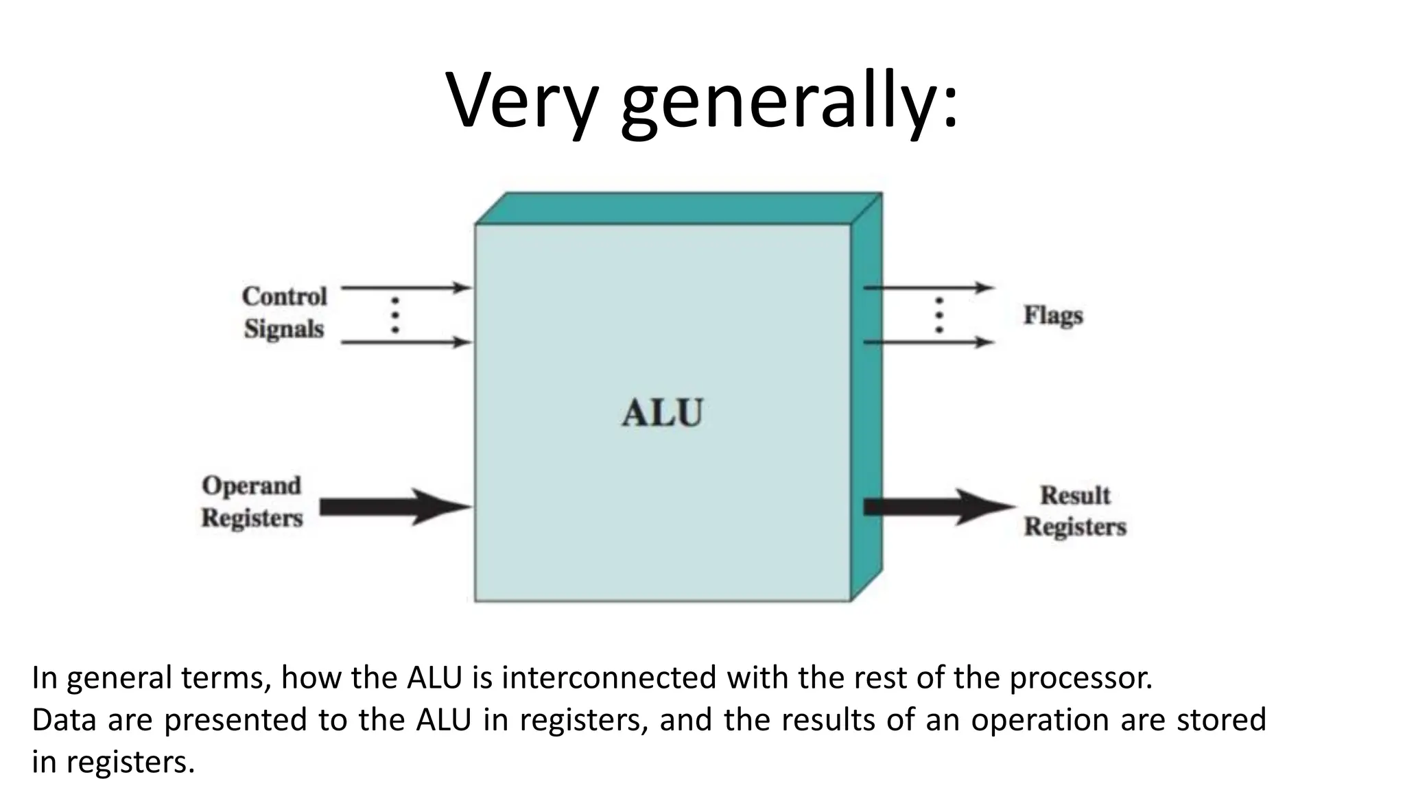
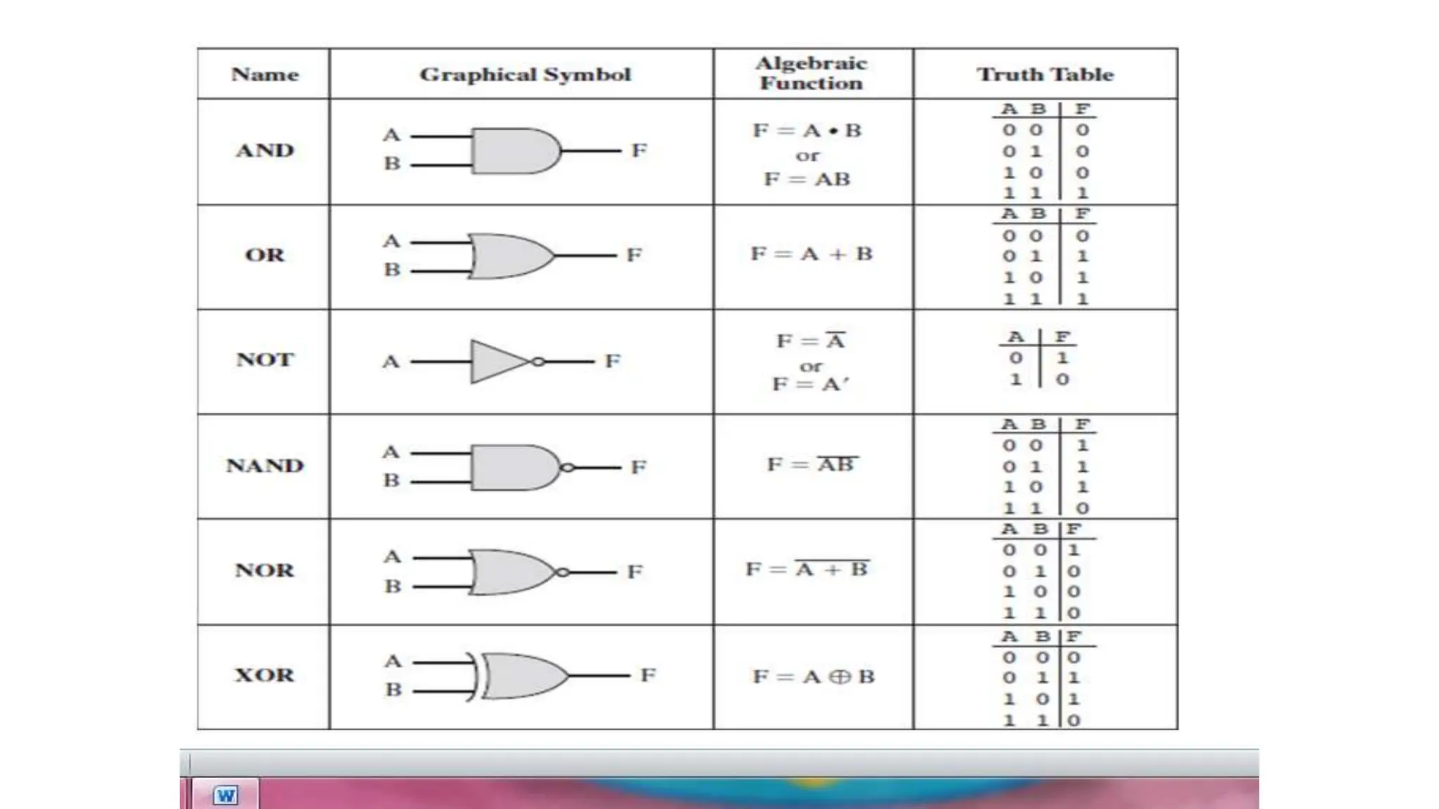
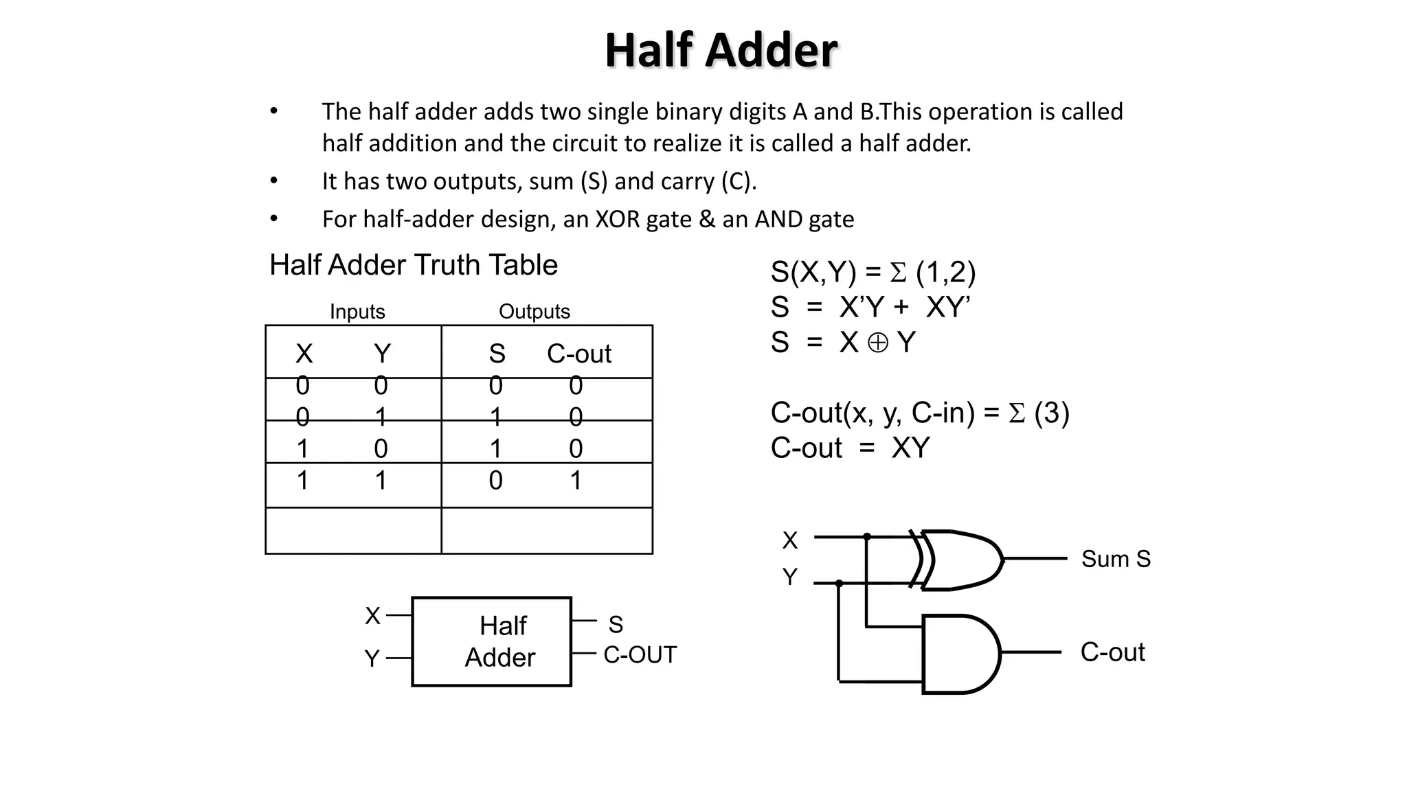
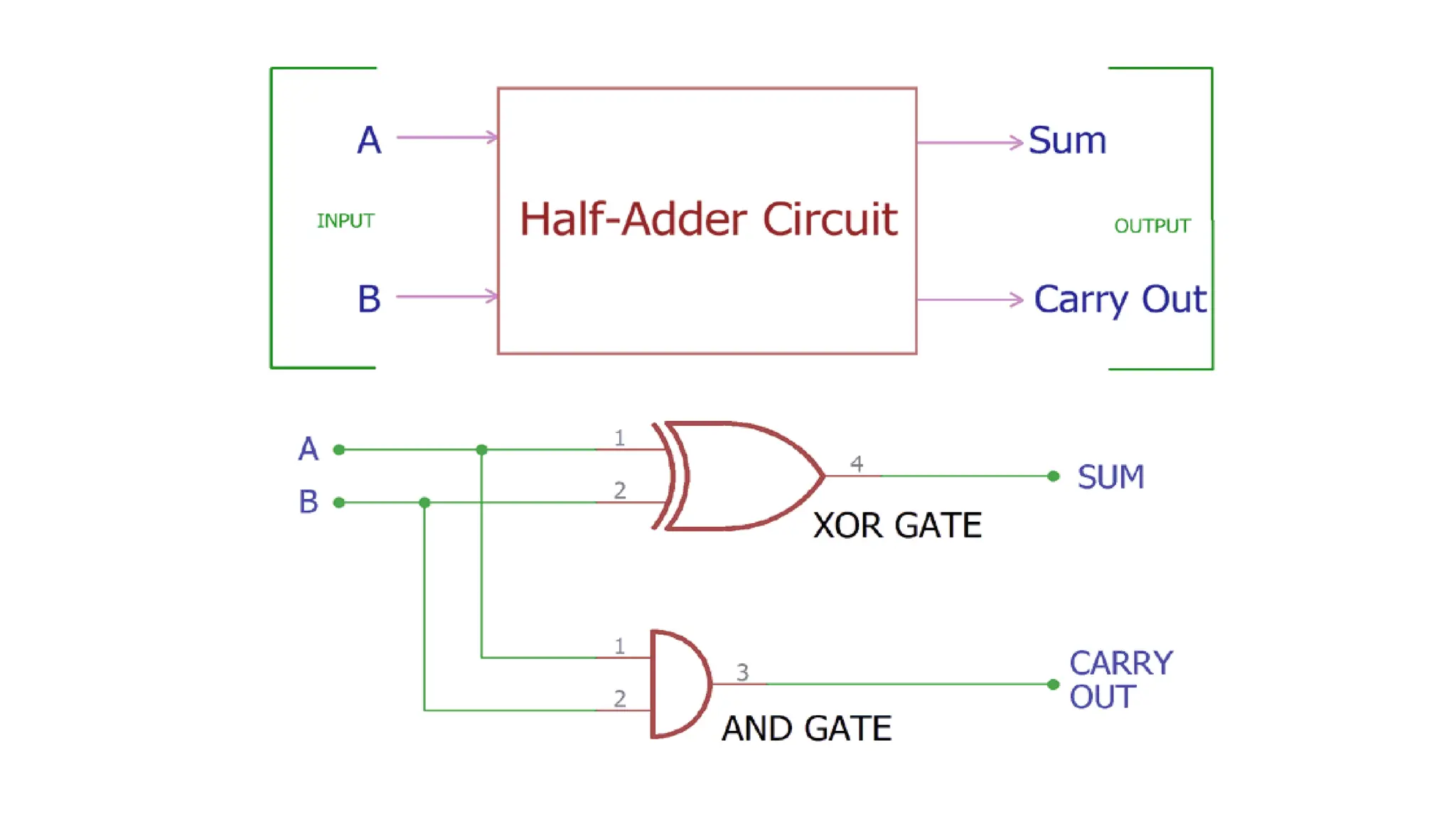
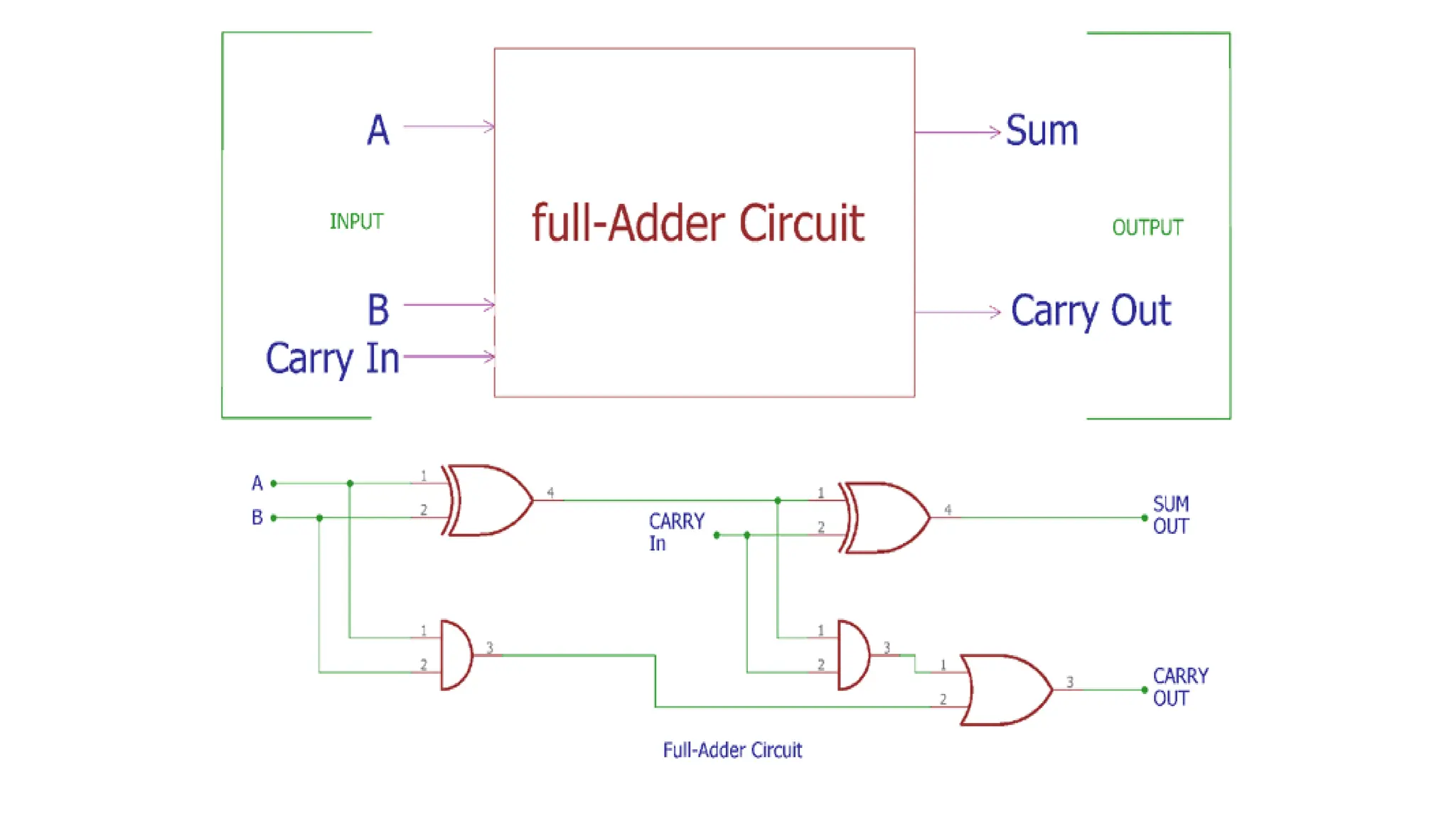
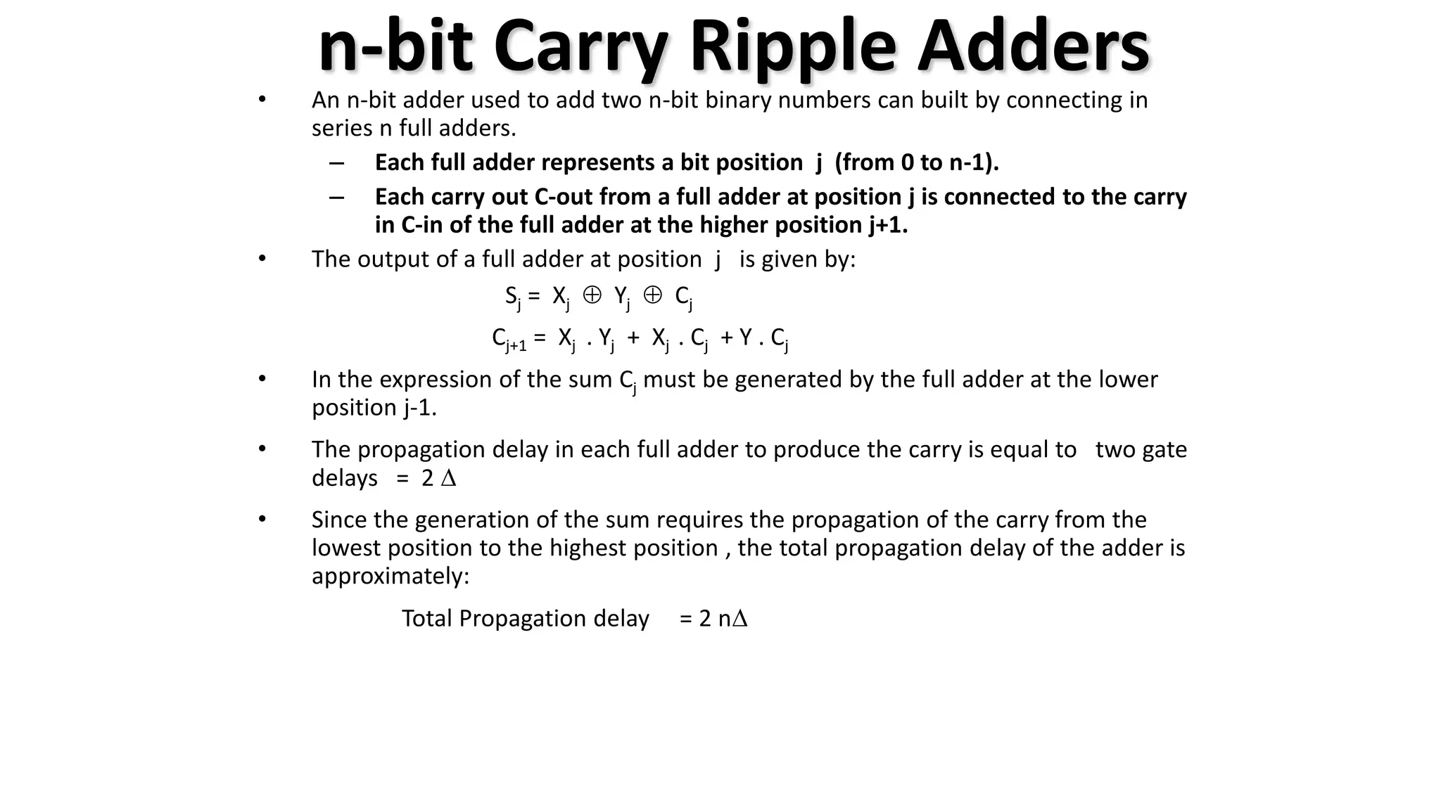
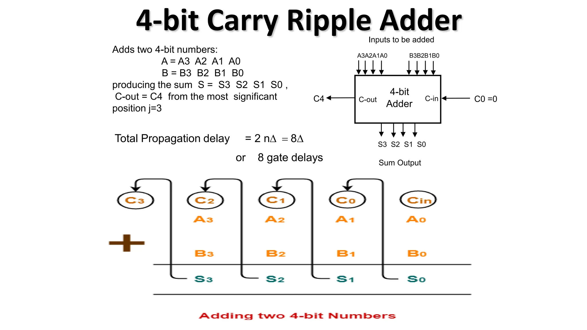
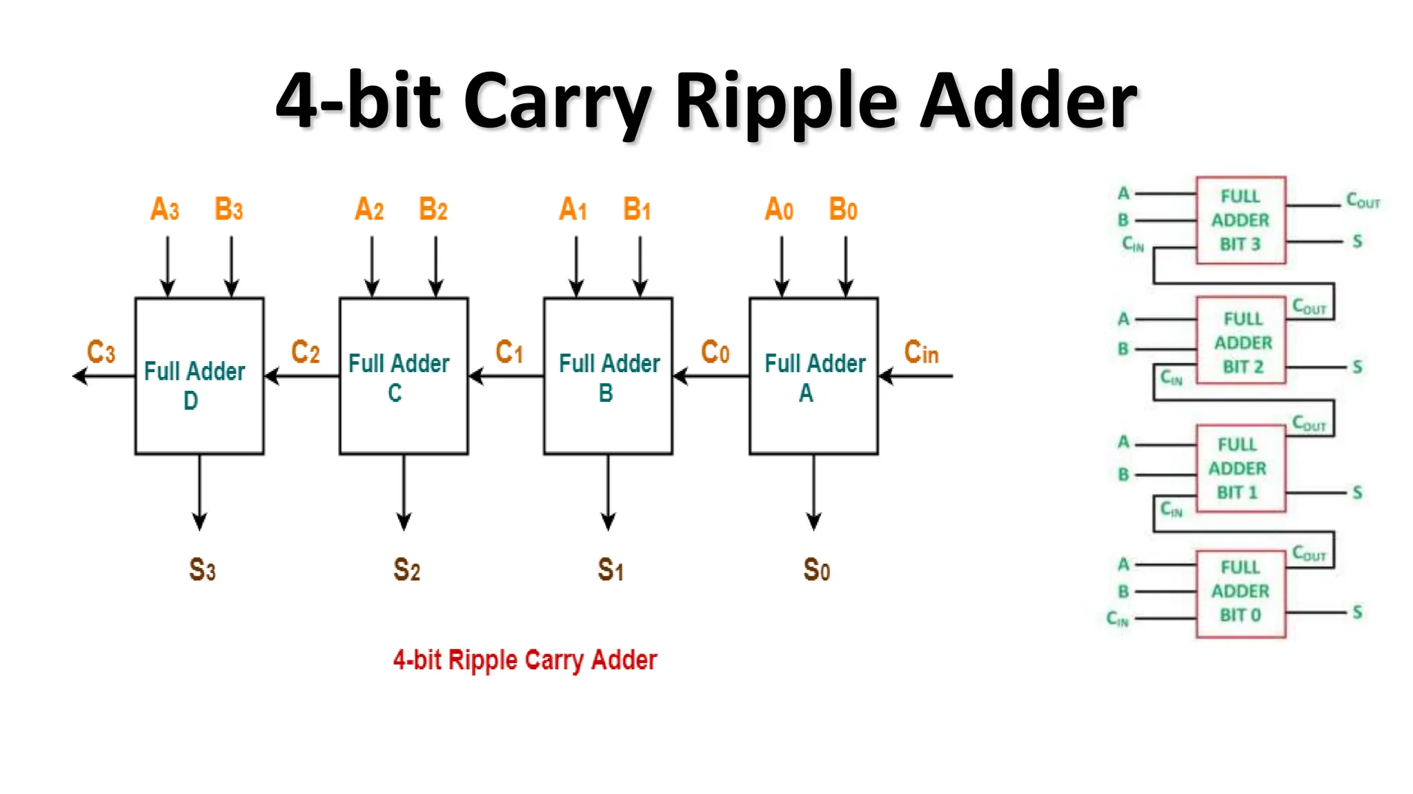
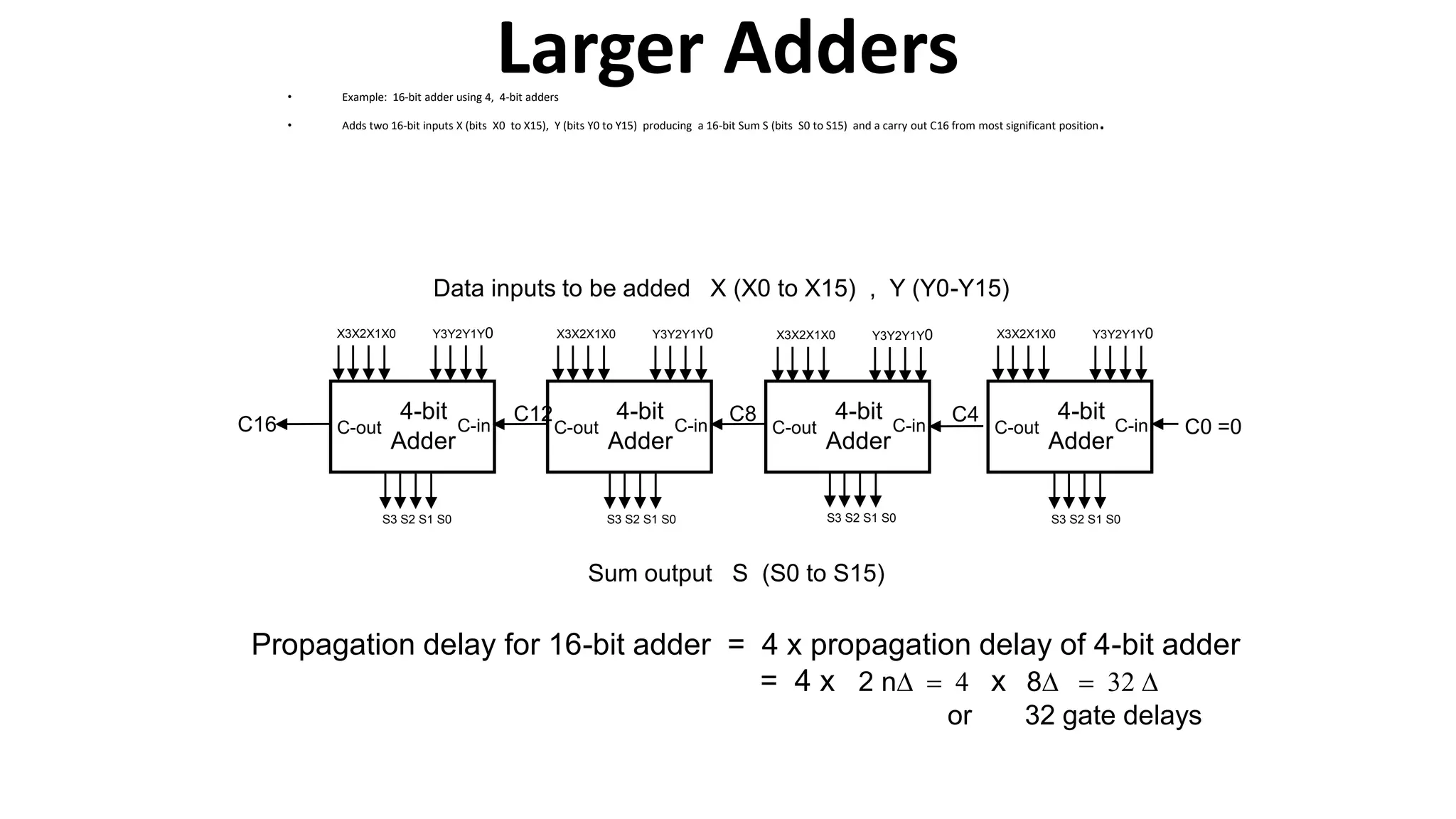
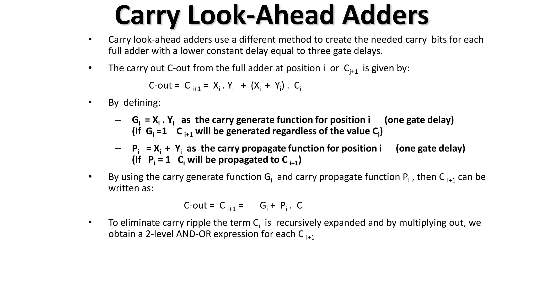
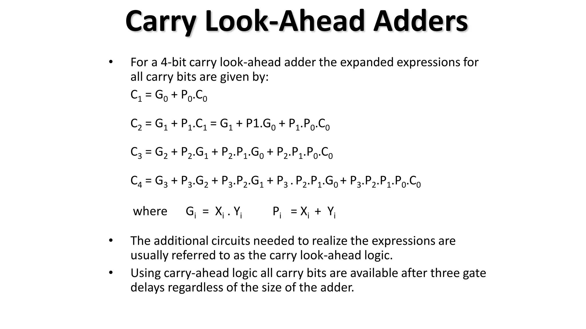
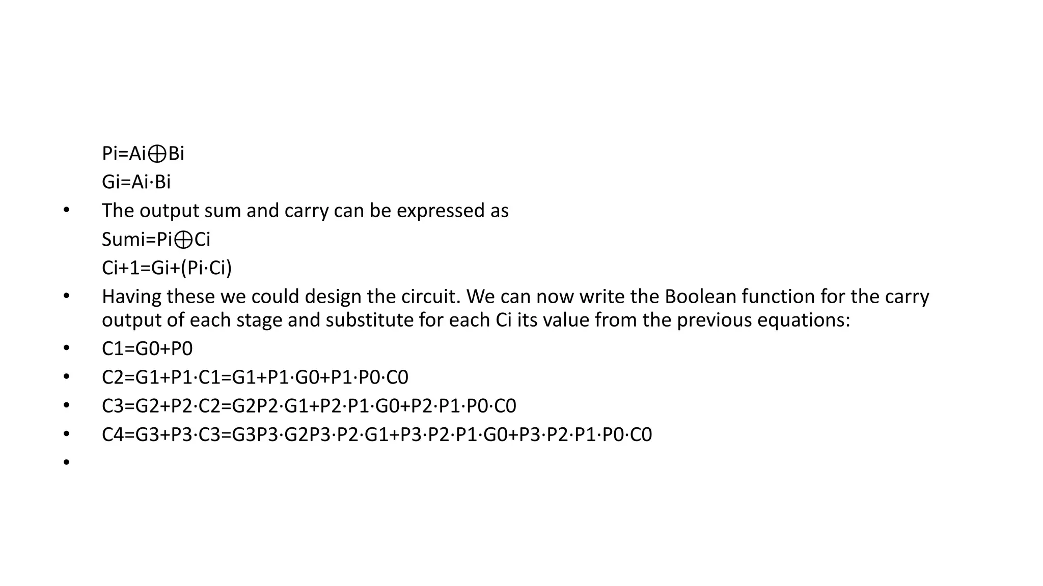
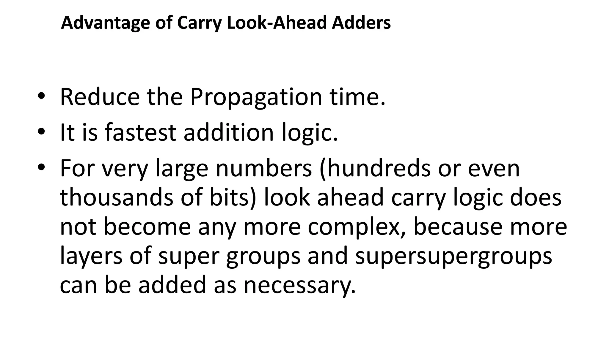
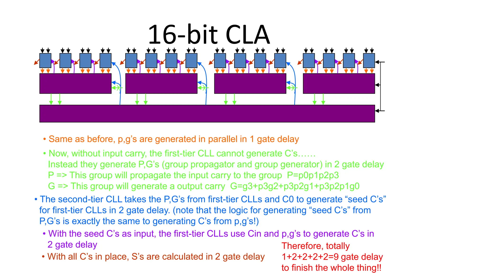
Computer Organization & Architecture
Unit-2 : Arithmetic and logic unit
By
Dr. B. K. Sharma
Professor & Head
Department of MCA
Ajay Kumar Garg Engineering College, Ghaziabad
Arithmetic logic unit(ALU)
• The ALU is that part of the computer that actually
performs arithmetic and logical operations on
data.
• All of the other elements of the computer
system—control unit, registers, memory, I/O—are
there mainly to bring data into the ALU for it to
process and then to take the results back out.
Very generally:
In general terms, how the ALU is interconnected with the rest of the processor.
Data are presented to the ALU in registers, and the results of an operation are stored
in registers.
Arithmetic logic unit
• An arithmetic logic unit is a combinational
digital electronic circuit that performs
arithmetic and bitwise operations on integer
binary numbers.
• This is in contrast to a floating-point unit,
which operates on floating point numbers
Logic gates
• Logic gates are the basic building blocks of any
digital system.
• It is an electronic circuit having one or more than
one input and only one output.
• The relationship between the input and the
output is based on a certain logic.
• Based on this, logic gates are named as
AND gate, OR gate, NOT gate etc.
Logic gates
• Logic circuits are represented by Boolean algebra
using variables and operators. The function and
variables have only one value, 0 and 1.
• The complement of a variable is shown by
an apostrophe (X’) or a bar over the letter such
as . Table below summarizes logic gates as the
symbol of the functions in Boolean expressions.
ADDER
• In electronics an adder is digital circuit that perform addition of
numbers.
• In modern computer adder reside in the arithmetic logic unit (ALU).
• In processor it is used to calculate addresses, table indices, and similar
operations.
• It can be constructed for many numerical representations, such as
binary-coded decimal or excess-3,the most common adders operate on
binary numbers.
TYPES OF ADDER
• Half Adder
• Full Adder
• Ripple Adder
• Look ahead carry Adder
Half Adder
• The half adder adds two single binary digits A and B.This operation is called
half addition and the circuit to realize it is called a half adder.
• It has two outputs, sum (S) and carry (C).
• For half-adder design, an XOR gate & an AND gate
X
0
0
1
1
Y
0
1
0
1
S
0
1
1
0
C-out
0
0
0
1
Half Adder Truth Table
Inputs Outputs
S(X,Y) = S (1,2)
S = X’Y + XY’
S = X  Y
C-out(x, y, C-in) = S (3)
C-out = XY
X
Y
Sum S
C-out
Half
Adder
X
Y
S
C-OUT
Full Adder
• Adding two single-bit binary values, X, Y with a carry input
bit C-in produces a sum bit S and a carry out C-out bit.
X
0
0
0
0
1
1
1
1
Y
0
0
1
1
0
0
1
1
S
0
1
1
0
1
0
0
1
C-out
0
0
0
1
0
1
1
1
C-in
0
1
0
1
0
1
0
1
Full Adder Truth Table
S(X,Y, C-in) = S (1,2,4,7)
C-out(x, y, C-in) = S (3,5,6,7)
Inputs Outputs
Sum S
C-in
X
0
1
00 01 11
10
Y
C-in
XY
0
1
2
3
6
7
4
5
1
1 1
1
C-in
X
0
1
00 01 11
10
Y
C-in
XY
0
1
2
3
6
7
4
5
1
1
1 1
Carry C-out
S = X’Y’(C-in) + XY’(C-in)’ + XY’(C-in)’ + XY(C-in)
S = X  Y  (C-in)
C-out = XY + X(C-in) + Y(C-in)
n-bit Carry Ripple Adders
• Ripple Carry Adder is a combinational logic
circuit.
• It is used for the purpose of adding two n-bit
binary numbers.
• It requires n full adders in its circuit for adding
two n-bit binary numbers.
• It is also known as n-bit parallel adder.
n-bit Carry Ripple Adders
• An n-bit adder used to add two n-bit binary numbers can built by connecting in
series n full adders.
– Each full adder represents a bit position j (from 0 to n-1).
– Each carry out C-out from a full adder at position j is connected to the carry
in C-in of the full adder at the higher position j+1.
• The output of a full adder at position j is given by:
Sj = Xj  Yj  Cj
Cj+1 = Xj . Yj + Xj . Cj + Y . Cj
• In the expression of the sum Cj must be generated by the full adder at the lower
position j-1.
• The propagation delay in each full adder to produce the carry is equal to two gate
delays = 2 D
• Since the generation of the sum requires the propagation of the carry from the
lowest position to the highest position , the total propagation delay of the adder is
approximately:
Total Propagation delay = 2 nD
4-bit Carry Ripple Adder
Adds two 4-bit numbers:
A = A3 A2 A1 A0
B = B3 B2 B1 B0
producing the sum S = S3 S2 S1 S0 ,
C-out = C4 from the most significant
position j=3
4-bit
Adder
A3A2A1A0
S3 S2 S1 S0
C-in
C-out
C4
B3B2B1B0
C0 =0
Inputs to be added
Sum Output
Total Propagation delay = 2 nD = 8D
or 8 gate delays
4-bit Carry Ripple Adder
Larger Adders
• Example: 16-bit adder using 4, 4-bit adders
• Adds two 16-bit inputs X (bits X0 to X15), Y (bits Y0 to Y15) producing a 16-bit Sum S (bits S0 to S15) and a carry out C16 from most significant position.
4-bit
Adder
C-in
C-out
4-bit
Adder
C-in
C-out C0 =0
4-bit
Adder
C-in
C-out
4-bit
Adder
C-in
C-out
C4
C8
C12
C16
Data inputs to be added X (X0 to X15) , Y (Y0-Y15)
Sum output S (S0 to S15)
Y3Y2Y1Y0
X3X2X1X0
Y3Y2Y1Y0
X3X2X1X0
Y3Y2Y1Y0
X3X2X1X0
Y3Y2Y1Y0
X3X2X1X0
S3 S2 S1 S0
S3 S2 S1 S0
S3 S2 S1 S0
S3 S2 S1 S0
Propagation delay for 16-bit adder = 4 x propagation delay of 4-bit adder
= 4 x 2 nD = 4 x 8D = 32 D
or 32 gate delays
Disadvantage of n-bit Carry Ripple Adder
• Each full adder has to necessarily wait until the
carry bit becomes available from its adjacent full
adder.
• This increases the propagation time.
• Due to this reason, ripple carry adder becomes
extremely slow.
• This is considered to be the biggest disadvantage
of using ripple carry adder.
Carry-Lookahead Adder
• The disadvantage of the ripple carry adder is that the propagation
delay of adder (2 nD ) increases as the size of the adder, n is increased
due to the carry ripple through all the full adders.
• The look ahead carry addition will therefore speed up the addition
process.
• The carry-lookahead adder calculates one or more carry bits before
the sum, which reduces the wait time to calculate the result of the
larger-value bits of the adder
Carry-lookahead adder
1. To reduce the computation time, there are faster ways to add two
binary numbers by using carry look ahead adders.
2. They work by creating two signals P and G known to be Carry
Propagator and Carry Generator.
3. The carry propagator is propagated to the next level whereas the carry
generator is used to generate the output carry, regardless of input
carry. The block diagram of a 4-bit Carry Look ahead Adder is shown
here below -
Carry-lookahead adder
4. The number of gate levels for the carry propagation can be found from the circuit
of full adder.
5. The signal from input carry Cin to output carry Cout requires an AND gate and an
OR gate, which constitutes two gate levels.
6. So if there are four full adders in the parallel adder, the output carry C5 would
have 2 X 4 = 8 gate levels from C1 to C5. For an n-bit parallel adder, there are 2n
gate levels to propagate through.
7. The corresponding Boolean expressions are given here to construct a carry look
ahead adder. In the carry look ahead circuit we need to generate the two signals
carry propagator (P) and carry generator (G),
Carry-lookahead adder
4-bit CLA
(+)
A0 B0
C0
(+)
A1 B1
(+)
A2 B2
(+)
A3 B3
CLL (carry look-ahead logic)
p0 g0
p1 g1
p2 g2
p3 g3
• Given A,B’s, all p,g’s are generated in 1 gate delay in parallel.
C1
C2
C3
• Given all p,g’s, all C’s are generated in 2 gate delay in parallel.
S3 S2 S1 S0
• Given all C’s, all S’s are generated in 2 gate delay in parallel.
• Key virtue of CLA: sequential operation in RCA is broken into parallel operation!!
Carry-lookahead adder
x
0
0
0
0
1
1
1
1
y
0
0
1
1
0
0
1
1
S
0
1
1
0
1
0
0
1
C-out
0
0
0
1
0
1
1
1
C-in
0
1
0
1
0
1
0
1
Full Adder Truth Table
C-out(x, y, C-in) = S (3,5,6,7)
Inputs Outputs
C-in
X
0
1
00 01 11 10
Y
C-in
XY
0
4
1
5
3
7
2
6
1
1
1 1
Carry C-out
C-out = XY + X(C-in) + Y(C-in)
C-out = XY + (X + Y) (C-in)
OR
C-out = XY (C-in) +XY (C-in)’ + XY’(C-in) + X’Y(C-in)
C-out = XY ( (C-in) +(C-in)’ ) + (XY’ + X’Y) (C-in)
C-out = XY + (X ⊕ Y) (C-in)
Carry Look-Ahead Adders
• Carry look-ahead adders use a different method to create the needed carry bits for each
full adder with a lower constant delay equal to three gate delays.
• The carry out C-out from the full adder at position i or Cj+1 is given by:
C-out = C i+1 = Xi . Yi + (Xi + Yi) . Ci
• By defining:
– Gi = Xi . Yi as the carry generate function for position i (one gate delay)
(If Gi =1 C i+1 will be generated regardless of the value Ci)
– Pi = Xi + Yi as the carry propagate function for position i (one gate delay)
(If Pi = 1 Ci will be propagated to C i+1)
• By using the carry generate function Gi and carry propagate function Pi , then C i+1 can be
written as:
C-out = C i+1 = Gi + Pi . Ci
• To eliminate carry ripple the term Ci is recursively expanded and by multiplying out, we
obtain a 2-level AND-OR expression for each C i+1
• For a 4-bit carry look-ahead adder the expanded expressions for
all carry bits are given by:
C1 = G0 + P0.C0
C2 = G1 + P1.C1 = G1 + P1.G0 + P1.P0.C0
C3 = G2 + P2.G1 + P2.P1.G0 + P2.P1.P0.C0
C4 = G3 + P3.G2 + P3.P2.G1 + P3 .P2.P1.G0 + P3.P2.P1.P0.C0
where Gi = Xi . Yi Pi = Xi + Yi
• The additional circuits needed to realize the expressions are
usually referred to as the carry look-ahead logic.
• Using carry-ahead logic all carry bits are available after three gate
delays regardless of the size of the adder.
Carry Look-Ahead Adders
Pi=Ai⊕Bi
Gi=Ai∙Bi
• The output sum and carry can be expressed as
Sumi=Pi⊕Ci
Ci+1=Gi+(Pi∙Ci)
• Having these we could design the circuit. We can now write the Boolean function for the carry
output of each stage and substitute for each Ci its value from the previous equations:
• C1=G0+P0
• C2=G1+P1∙C1=G1+P1∙G0+P1∙P0∙C0
• C3=G2+P2∙C2=G2P2∙G1+P2∙P1∙G0+P2∙P1∙P0∙C0
• C4=G3+P3∙C3=G3P3∙G2P3∙P2∙G1+P3∙P2∙P1∙G0+P3∙P2∙P1∙P0∙C0
•
Advantage of Carry Look-Ahead Adders
• Reduce the Propagation time.
• It is fastest addition logic.
• For very large numbers (hundreds or even
thousands of bits) look ahead carry logic does
not become any more complex, because more
layers of super groups and supersupergroups
can be added as necessary.
16-bit CLA
• Same as before, p,g’s are generated in parallel in 1 gate delay
• The second-tier CLL takes the P,G’s from first-tier CLLs and C0 to generate “seed C’s”
for first-tier CLLs in 2 gate delay. (note that the logic for generating “seed C’s” from
P,G’s is exactly the same to generating C’s from p,g’s!)
• With the seed C’s as input, the first-tier CLLs use Cin and p,g’s to generate C’s in
2 gate delay
• With all C’s in place, S’s are calculated in 2 gate delay
Therefore, totally
1+2+2+2+2=9 gate delay
to finish the whole thing!!
• Now, without input carry, the first-tier CLL cannot generate C’s……
Instead they generate P,G’s (group propagator and group generator) in 2 gate delay
P => This group will propagate the input carry to the group P=p0p1p2p3
G => This group will generate a output carry G=g3+p3g2+p3p2g1+p3p2p1g0
Now, how about 64-bit CLA?
• You can visualize that in mind by yourself now,
I guess.
Thanks!!

Computer Organization and Architecture Presentation

  • 1.
    Computer Organization &Architecture Unit-2 : Arithmetic and logic unit By Dr. B. K. Sharma Professor & Head Department of MCA Ajay Kumar Garg Engineering College, Ghaziabad
  • 2.
    Arithmetic logic unit(ALU) •The ALU is that part of the computer that actually performs arithmetic and logical operations on data. • All of the other elements of the computer system—control unit, registers, memory, I/O—are there mainly to bring data into the ALU for it to process and then to take the results back out.
  • 3.
    Very generally: In generalterms, how the ALU is interconnected with the rest of the processor. Data are presented to the ALU in registers, and the results of an operation are stored in registers.
  • 4.
    Arithmetic logic unit •An arithmetic logic unit is a combinational digital electronic circuit that performs arithmetic and bitwise operations on integer binary numbers. • This is in contrast to a floating-point unit, which operates on floating point numbers
  • 5.
    Logic gates • Logicgates are the basic building blocks of any digital system. • It is an electronic circuit having one or more than one input and only one output. • The relationship between the input and the output is based on a certain logic. • Based on this, logic gates are named as AND gate, OR gate, NOT gate etc.
  • 6.
    Logic gates • Logiccircuits are represented by Boolean algebra using variables and operators. The function and variables have only one value, 0 and 1. • The complement of a variable is shown by an apostrophe (X’) or a bar over the letter such as . Table below summarizes logic gates as the symbol of the functions in Boolean expressions.
  • 8.
    ADDER • In electronicsan adder is digital circuit that perform addition of numbers. • In modern computer adder reside in the arithmetic logic unit (ALU). • In processor it is used to calculate addresses, table indices, and similar operations. • It can be constructed for many numerical representations, such as binary-coded decimal or excess-3,the most common adders operate on binary numbers.
  • 9.
    TYPES OF ADDER •Half Adder • Full Adder • Ripple Adder • Look ahead carry Adder
  • 10.
    Half Adder • Thehalf adder adds two single binary digits A and B.This operation is called half addition and the circuit to realize it is called a half adder. • It has two outputs, sum (S) and carry (C). • For half-adder design, an XOR gate & an AND gate X 0 0 1 1 Y 0 1 0 1 S 0 1 1 0 C-out 0 0 0 1 Half Adder Truth Table Inputs Outputs S(X,Y) = S (1,2) S = X’Y + XY’ S = X  Y C-out(x, y, C-in) = S (3) C-out = XY X Y Sum S C-out Half Adder X Y S C-OUT
  • 12.
    Full Adder • Addingtwo single-bit binary values, X, Y with a carry input bit C-in produces a sum bit S and a carry out C-out bit. X 0 0 0 0 1 1 1 1 Y 0 0 1 1 0 0 1 1 S 0 1 1 0 1 0 0 1 C-out 0 0 0 1 0 1 1 1 C-in 0 1 0 1 0 1 0 1 Full Adder Truth Table S(X,Y, C-in) = S (1,2,4,7) C-out(x, y, C-in) = S (3,5,6,7) Inputs Outputs Sum S C-in X 0 1 00 01 11 10 Y C-in XY 0 1 2 3 6 7 4 5 1 1 1 1 C-in X 0 1 00 01 11 10 Y C-in XY 0 1 2 3 6 7 4 5 1 1 1 1 Carry C-out S = X’Y’(C-in) + XY’(C-in)’ + XY’(C-in)’ + XY(C-in) S = X  Y  (C-in) C-out = XY + X(C-in) + Y(C-in)
  • 14.
    n-bit Carry RippleAdders • Ripple Carry Adder is a combinational logic circuit. • It is used for the purpose of adding two n-bit binary numbers. • It requires n full adders in its circuit for adding two n-bit binary numbers. • It is also known as n-bit parallel adder.
  • 15.
    n-bit Carry RippleAdders • An n-bit adder used to add two n-bit binary numbers can built by connecting in series n full adders. – Each full adder represents a bit position j (from 0 to n-1). – Each carry out C-out from a full adder at position j is connected to the carry in C-in of the full adder at the higher position j+1. • The output of a full adder at position j is given by: Sj = Xj  Yj  Cj Cj+1 = Xj . Yj + Xj . Cj + Y . Cj • In the expression of the sum Cj must be generated by the full adder at the lower position j-1. • The propagation delay in each full adder to produce the carry is equal to two gate delays = 2 D • Since the generation of the sum requires the propagation of the carry from the lowest position to the highest position , the total propagation delay of the adder is approximately: Total Propagation delay = 2 nD
  • 16.
    4-bit Carry RippleAdder Adds two 4-bit numbers: A = A3 A2 A1 A0 B = B3 B2 B1 B0 producing the sum S = S3 S2 S1 S0 , C-out = C4 from the most significant position j=3 4-bit Adder A3A2A1A0 S3 S2 S1 S0 C-in C-out C4 B3B2B1B0 C0 =0 Inputs to be added Sum Output Total Propagation delay = 2 nD = 8D or 8 gate delays
  • 17.
  • 18.
    Larger Adders • Example:16-bit adder using 4, 4-bit adders • Adds two 16-bit inputs X (bits X0 to X15), Y (bits Y0 to Y15) producing a 16-bit Sum S (bits S0 to S15) and a carry out C16 from most significant position. 4-bit Adder C-in C-out 4-bit Adder C-in C-out C0 =0 4-bit Adder C-in C-out 4-bit Adder C-in C-out C4 C8 C12 C16 Data inputs to be added X (X0 to X15) , Y (Y0-Y15) Sum output S (S0 to S15) Y3Y2Y1Y0 X3X2X1X0 Y3Y2Y1Y0 X3X2X1X0 Y3Y2Y1Y0 X3X2X1X0 Y3Y2Y1Y0 X3X2X1X0 S3 S2 S1 S0 S3 S2 S1 S0 S3 S2 S1 S0 S3 S2 S1 S0 Propagation delay for 16-bit adder = 4 x propagation delay of 4-bit adder = 4 x 2 nD = 4 x 8D = 32 D or 32 gate delays
  • 19.
    Disadvantage of n-bitCarry Ripple Adder • Each full adder has to necessarily wait until the carry bit becomes available from its adjacent full adder. • This increases the propagation time. • Due to this reason, ripple carry adder becomes extremely slow. • This is considered to be the biggest disadvantage of using ripple carry adder.
  • 20.
    Carry-Lookahead Adder • Thedisadvantage of the ripple carry adder is that the propagation delay of adder (2 nD ) increases as the size of the adder, n is increased due to the carry ripple through all the full adders. • The look ahead carry addition will therefore speed up the addition process. • The carry-lookahead adder calculates one or more carry bits before the sum, which reduces the wait time to calculate the result of the larger-value bits of the adder
  • 21.
    Carry-lookahead adder 1. Toreduce the computation time, there are faster ways to add two binary numbers by using carry look ahead adders. 2. They work by creating two signals P and G known to be Carry Propagator and Carry Generator. 3. The carry propagator is propagated to the next level whereas the carry generator is used to generate the output carry, regardless of input carry. The block diagram of a 4-bit Carry Look ahead Adder is shown here below -
  • 22.
    Carry-lookahead adder 4. Thenumber of gate levels for the carry propagation can be found from the circuit of full adder. 5. The signal from input carry Cin to output carry Cout requires an AND gate and an OR gate, which constitutes two gate levels. 6. So if there are four full adders in the parallel adder, the output carry C5 would have 2 X 4 = 8 gate levels from C1 to C5. For an n-bit parallel adder, there are 2n gate levels to propagate through. 7. The corresponding Boolean expressions are given here to construct a carry look ahead adder. In the carry look ahead circuit we need to generate the two signals carry propagator (P) and carry generator (G),
  • 23.
  • 24.
    4-bit CLA (+) A0 B0 C0 (+) A1B1 (+) A2 B2 (+) A3 B3 CLL (carry look-ahead logic) p0 g0 p1 g1 p2 g2 p3 g3 • Given A,B’s, all p,g’s are generated in 1 gate delay in parallel. C1 C2 C3 • Given all p,g’s, all C’s are generated in 2 gate delay in parallel. S3 S2 S1 S0 • Given all C’s, all S’s are generated in 2 gate delay in parallel. • Key virtue of CLA: sequential operation in RCA is broken into parallel operation!!
  • 25.
    Carry-lookahead adder x 0 0 0 0 1 1 1 1 y 0 0 1 1 0 0 1 1 S 0 1 1 0 1 0 0 1 C-out 0 0 0 1 0 1 1 1 C-in 0 1 0 1 0 1 0 1 Full AdderTruth Table C-out(x, y, C-in) = S (3,5,6,7) Inputs Outputs C-in X 0 1 00 01 11 10 Y C-in XY 0 4 1 5 3 7 2 6 1 1 1 1 Carry C-out C-out = XY + X(C-in) + Y(C-in) C-out = XY + (X + Y) (C-in) OR C-out = XY (C-in) +XY (C-in)’ + XY’(C-in) + X’Y(C-in) C-out = XY ( (C-in) +(C-in)’ ) + (XY’ + X’Y) (C-in) C-out = XY + (X ⊕ Y) (C-in)
  • 26.
    Carry Look-Ahead Adders •Carry look-ahead adders use a different method to create the needed carry bits for each full adder with a lower constant delay equal to three gate delays. • The carry out C-out from the full adder at position i or Cj+1 is given by: C-out = C i+1 = Xi . Yi + (Xi + Yi) . Ci • By defining: – Gi = Xi . Yi as the carry generate function for position i (one gate delay) (If Gi =1 C i+1 will be generated regardless of the value Ci) – Pi = Xi + Yi as the carry propagate function for position i (one gate delay) (If Pi = 1 Ci will be propagated to C i+1) • By using the carry generate function Gi and carry propagate function Pi , then C i+1 can be written as: C-out = C i+1 = Gi + Pi . Ci • To eliminate carry ripple the term Ci is recursively expanded and by multiplying out, we obtain a 2-level AND-OR expression for each C i+1
  • 27.
    • For a4-bit carry look-ahead adder the expanded expressions for all carry bits are given by: C1 = G0 + P0.C0 C2 = G1 + P1.C1 = G1 + P1.G0 + P1.P0.C0 C3 = G2 + P2.G1 + P2.P1.G0 + P2.P1.P0.C0 C4 = G3 + P3.G2 + P3.P2.G1 + P3 .P2.P1.G0 + P3.P2.P1.P0.C0 where Gi = Xi . Yi Pi = Xi + Yi • The additional circuits needed to realize the expressions are usually referred to as the carry look-ahead logic. • Using carry-ahead logic all carry bits are available after three gate delays regardless of the size of the adder. Carry Look-Ahead Adders
  • 28.
    Pi=Ai⊕Bi Gi=Ai∙Bi • The outputsum and carry can be expressed as Sumi=Pi⊕Ci Ci+1=Gi+(Pi∙Ci) • Having these we could design the circuit. We can now write the Boolean function for the carry output of each stage and substitute for each Ci its value from the previous equations: • C1=G0+P0 • C2=G1+P1∙C1=G1+P1∙G0+P1∙P0∙C0 • C3=G2+P2∙C2=G2P2∙G1+P2∙P1∙G0+P2∙P1∙P0∙C0 • C4=G3+P3∙C3=G3P3∙G2P3∙P2∙G1+P3∙P2∙P1∙G0+P3∙P2∙P1∙P0∙C0 •
  • 29.
    Advantage of CarryLook-Ahead Adders • Reduce the Propagation time. • It is fastest addition logic. • For very large numbers (hundreds or even thousands of bits) look ahead carry logic does not become any more complex, because more layers of super groups and supersupergroups can be added as necessary.
  • 30.
    16-bit CLA • Sameas before, p,g’s are generated in parallel in 1 gate delay • The second-tier CLL takes the P,G’s from first-tier CLLs and C0 to generate “seed C’s” for first-tier CLLs in 2 gate delay. (note that the logic for generating “seed C’s” from P,G’s is exactly the same to generating C’s from p,g’s!) • With the seed C’s as input, the first-tier CLLs use Cin and p,g’s to generate C’s in 2 gate delay • With all C’s in place, S’s are calculated in 2 gate delay Therefore, totally 1+2+2+2+2=9 gate delay to finish the whole thing!! • Now, without input carry, the first-tier CLL cannot generate C’s…… Instead they generate P,G’s (group propagator and group generator) in 2 gate delay P => This group will propagate the input carry to the group P=p0p1p2p3 G => This group will generate a output carry G=g3+p3g2+p3p2g1+p3p2p1g0
  • 31.
    Now, how about64-bit CLA? • You can visualize that in mind by yourself now, I guess.
  • 32.