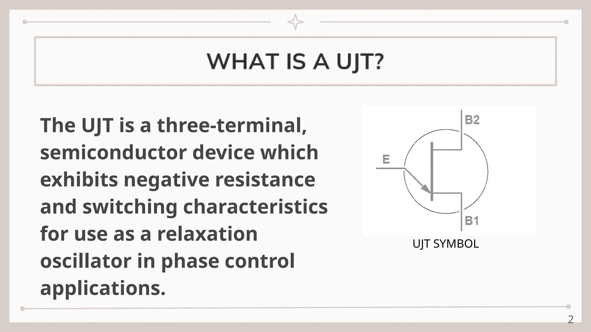
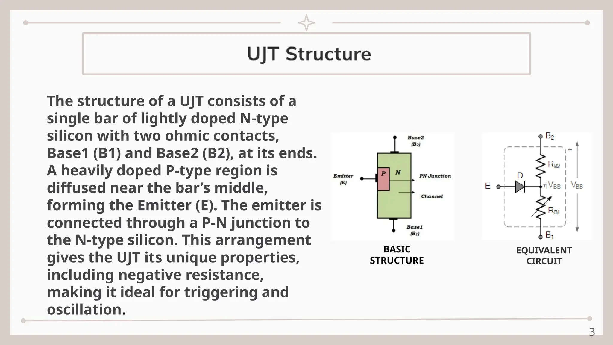
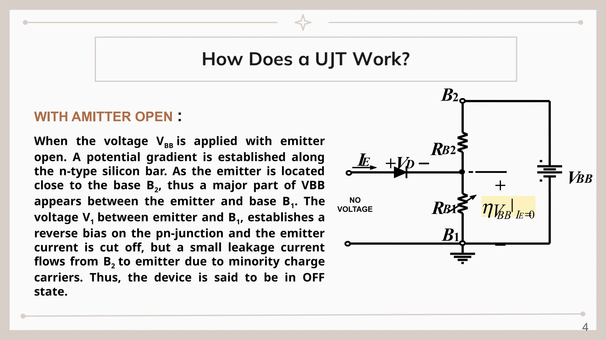
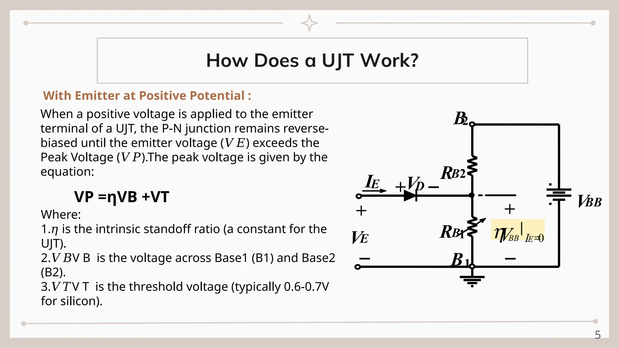
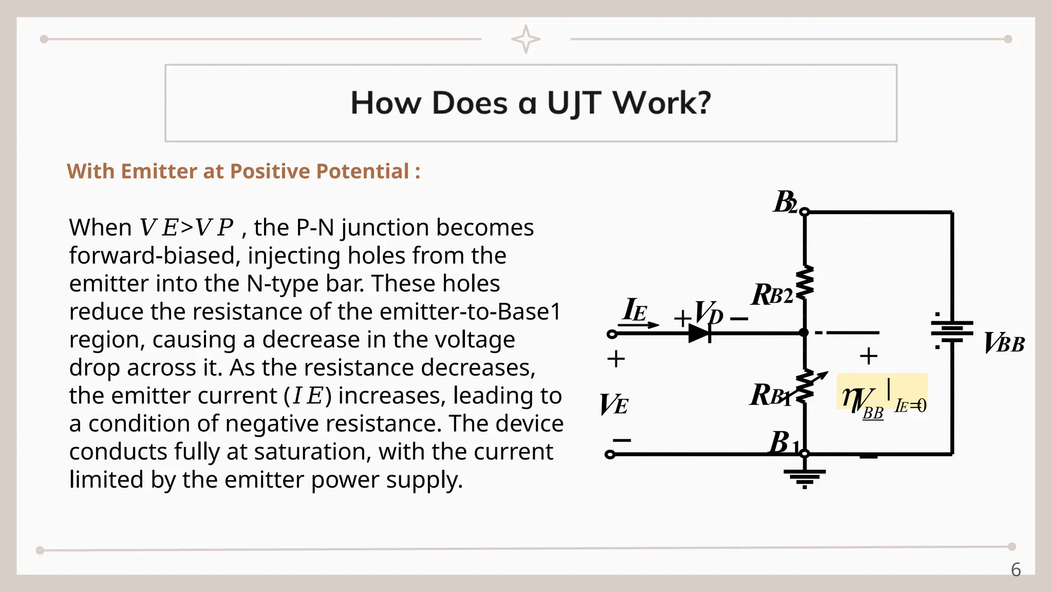
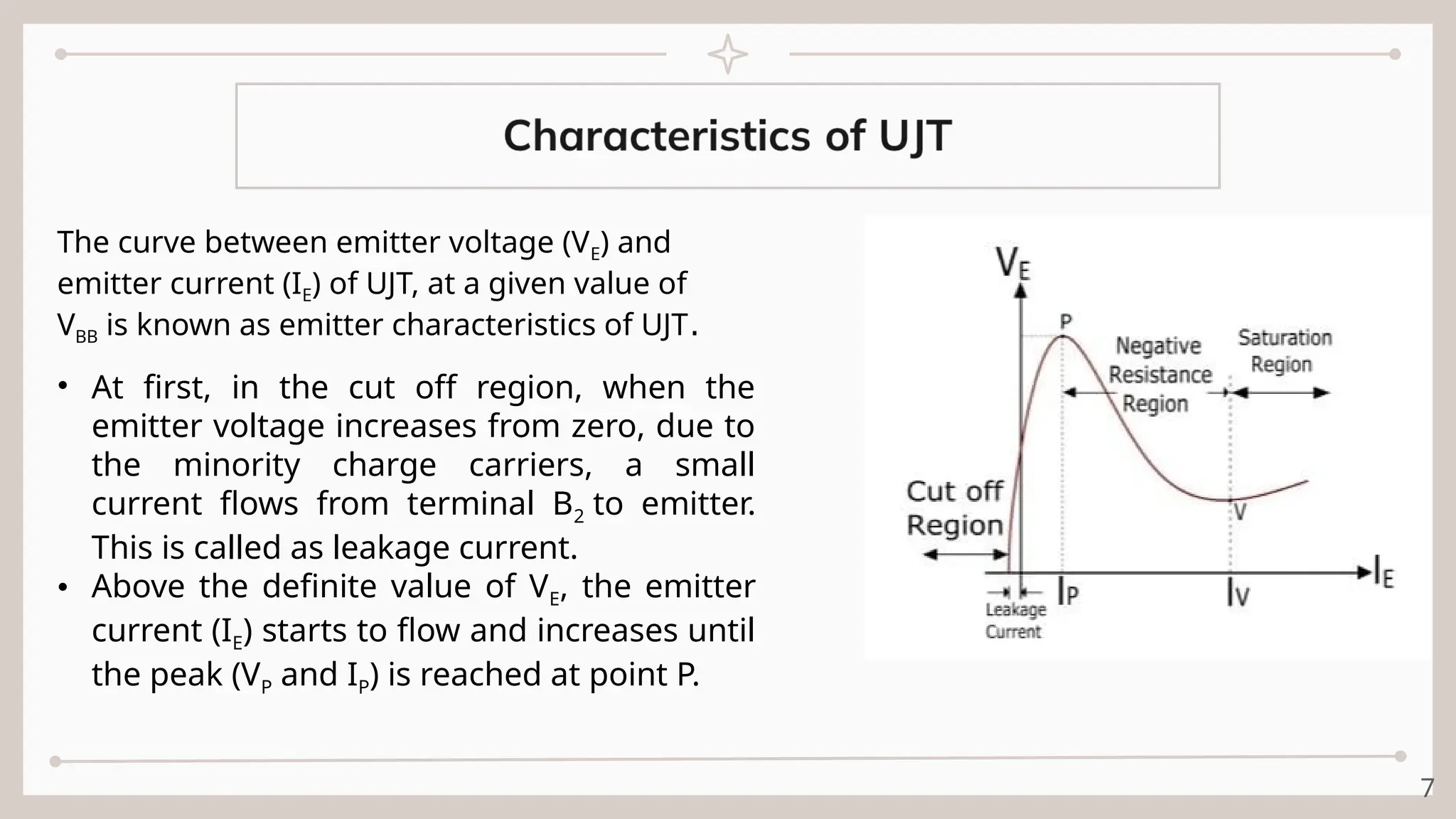
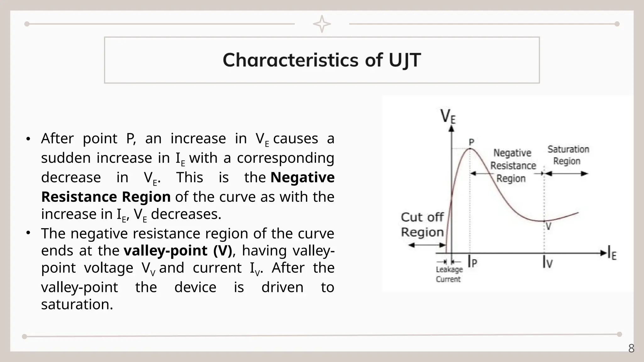
Unijunction
Transistor
SUBMITTED BY
MAHFUZ HOSSAIN ANTOR
24524203158
CSE-BUP
SUBMITTED TO
Md. Sazzadur Rahman, Ph.D
Professor
IIT-JU
2
The UJT is a three-terminal,
semiconductor device which
exhibits negative resistance
and switching characteristics
for use as a relaxation
oscillator in phase control
applications.
UJT SYMBOL
3
The structure of a UJT consists of a
single bar of lightly doped N-type
silicon with two ohmic contacts,
Base1 (B1) and Base2 (B2), at its ends.
A heavily doped P-type region is
diffused near the bar’s middle,
forming the Emitter (E). The emitter is
connected through a P-N junction to
the N-type silicon. This arrangement
gives the UJT its unique properties,
including negative resistance,
making it ideal for triggering and
oscillation.
BASIC
STRUCTURE
EQUIVALENT
CIRCUIT
4
RB2
RB1
VBB
0
=
E
I
BB
V
h
+VD -
IE
-
B2
B1
+
-
When the voltage VBB is applied with emitter
open. A potential gradient is established along
the n-type silicon bar. As the emitter is located
close to the base B2, thus a major part of VBB
appears between the emitter and base B1. The
voltage V1 between emitter and B1, establishes a
reverse bias on the pn-junction and the emitter
current is cut off, but a small leakage current
flows from B2 to emitter due to minority charge
carriers. Thus, the device is said to be in OFF
state.
NO
VOLTAGE
WITH AMITTER OPEN :
5
RB2
RB1
VBB
0
=
E
I
BB
V
h
+VD -
IE
+
VE
-
B
2
B1
+
-
With Emitter at Positive Potential :
When a positive voltage is applied to the emitter
terminal of a UJT, the P-N junction remains reverse-
biased until the emitter voltage ( ) exceeds the
𝑉𝐸
Peak Voltage ( ).The peak voltage is given by the
𝑉𝑃
equation:
VP​=ηVB​+VT​
Where:
1. is the intrinsic standoff ratio (a constant for the
𝜂
UJT).
2. V B​ is the voltage across Base1 (B1) and Base2
𝑉𝐵
(B2).
3. V T​ is the threshold voltage (typically 0.6-0.7V
𝑉𝑇
for silicon).
6
RB2
RB1
VBB
0
=
E
I
BB
V
h
+VD -
IE
+
VE
-
B
2
B1
+
-
With Emitter at Positive Potential :
When > ​, the P-N junction becomes
𝑉𝐸 𝑉𝑃
forward-biased, injecting holes from the
emitter into the N-type bar. These holes
reduce the resistance of the emitter-to-Base1
region, causing a decrease in the voltage
drop across it. As the resistance decreases,
the emitter current ( ) increases, leading to
𝐼𝐸
a condition of negative resistance. The device
conducts fully at saturation, with the current
limited by the emitter power supply.
7
The curve between emitter voltage (VE) and
emitter current (IE) of UJT, at a given value of
VBB is known as emitter characteristics of UJT.
• At first, in the cut off region, when the
emitter voltage increases from zero, due to
the minority charge carriers, a small
current flows from terminal B2 to emitter.
This is called as leakage current.
• Above the definite value of VE, the emitter
current (IE) starts to flow and increases until
the peak (VP and IP) is reached at point P.
8
• After point P, an increase in VE causes a
sudden increase in IE with a corresponding
decrease in VE. This is the Negative
Resistance Region of the curve as with the
increase in IE, VE decreases.
• The negative resistance region of the curve
ends at the valley-point (V), having valley-
point voltage VV and current IV. After the
valley-point the device is driven to
saturation.
9
•Simple Construction
•Low Power Consumption
•Reliable Triggering
•Negative Resistance Property
•Wide Operating Range
•High Efficiency
• Oscillators
• Trigger Circuits
• Saw tooth generator
• Bi-stable networks
• Pulse and voltage sensing circuits
• UJT relaxation oscillators
• Over voltage detectors
10
ANY QUERIES?

A presentation On ujt using transistor circuut

  • 1.
    Unijunction Transistor SUBMITTED BY MAHFUZ HOSSAINANTOR 24524203158 CSE-BUP SUBMITTED TO Md. Sazzadur Rahman, Ph.D Professor IIT-JU
  • 2.
    2 The UJT isa three-terminal, semiconductor device which exhibits negative resistance and switching characteristics for use as a relaxation oscillator in phase control applications. UJT SYMBOL
  • 3.
    3 The structure ofa UJT consists of a single bar of lightly doped N-type silicon with two ohmic contacts, Base1 (B1) and Base2 (B2), at its ends. A heavily doped P-type region is diffused near the bar’s middle, forming the Emitter (E). The emitter is connected through a P-N junction to the N-type silicon. This arrangement gives the UJT its unique properties, including negative resistance, making it ideal for triggering and oscillation. BASIC STRUCTURE EQUIVALENT CIRCUIT
  • 4.
    4 RB2 RB1 VBB 0 = E I BB V h +VD - IE - B2 B1 + - When thevoltage VBB is applied with emitter open. A potential gradient is established along the n-type silicon bar. As the emitter is located close to the base B2, thus a major part of VBB appears between the emitter and base B1. The voltage V1 between emitter and B1, establishes a reverse bias on the pn-junction and the emitter current is cut off, but a small leakage current flows from B2 to emitter due to minority charge carriers. Thus, the device is said to be in OFF state. NO VOLTAGE WITH AMITTER OPEN :
  • 5.
    5 RB2 RB1 VBB 0 = E I BB V h +VD - IE + VE - B 2 B1 + - With Emitterat Positive Potential : When a positive voltage is applied to the emitter terminal of a UJT, the P-N junction remains reverse- biased until the emitter voltage ( ) exceeds the 𝑉𝐸 Peak Voltage ( ).The peak voltage is given by the 𝑉𝑃 equation: VP​=ηVB​+VT​ Where: 1. is the intrinsic standoff ratio (a constant for the 𝜂 UJT). 2. V B​ is the voltage across Base1 (B1) and Base2 𝑉𝐵 (B2). 3. V T​ is the threshold voltage (typically 0.6-0.7V 𝑉𝑇 for silicon).
  • 6.
    6 RB2 RB1 VBB 0 = E I BB V h +VD - IE + VE - B 2 B1 + - With Emitterat Positive Potential : When > ​, the P-N junction becomes 𝑉𝐸 𝑉𝑃 forward-biased, injecting holes from the emitter into the N-type bar. These holes reduce the resistance of the emitter-to-Base1 region, causing a decrease in the voltage drop across it. As the resistance decreases, the emitter current ( ) increases, leading to 𝐼𝐸 a condition of negative resistance. The device conducts fully at saturation, with the current limited by the emitter power supply.
  • 7.
    7 The curve betweenemitter voltage (VE) and emitter current (IE) of UJT, at a given value of VBB is known as emitter characteristics of UJT. • At first, in the cut off region, when the emitter voltage increases from zero, due to the minority charge carriers, a small current flows from terminal B2 to emitter. This is called as leakage current. • Above the definite value of VE, the emitter current (IE) starts to flow and increases until the peak (VP and IP) is reached at point P.
  • 8.
    8 • After pointP, an increase in VE causes a sudden increase in IE with a corresponding decrease in VE. This is the Negative Resistance Region of the curve as with the increase in IE, VE decreases. • The negative resistance region of the curve ends at the valley-point (V), having valley- point voltage VV and current IV. After the valley-point the device is driven to saturation.
  • 9.
    9 •Simple Construction •Low PowerConsumption •Reliable Triggering •Negative Resistance Property •Wide Operating Range •High Efficiency • Oscillators • Trigger Circuits • Saw tooth generator • Bi-stable networks • Pulse and voltage sensing circuits • UJT relaxation oscillators • Over voltage detectors
  • 10.