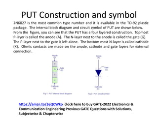
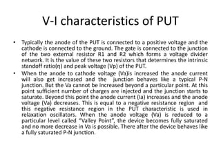
Programmable
UJT (PUT)
Rashmi Patil
https://amzn.to/3eQCWko clock here to buy GATE-2022 Electronics & Communication
Engineering Previous GATE Questions with Solutions, Subjectwise & Chapterwise
• Programmable unijunction transistor or PUT is a close
relative of the thyristor family.
• Its has a four layered construction just like the thyristors
and have three terminals named anode(A), cathode(K) and
gate(G) again like the thyristors. Y
• et some authors call it a programmable UJT just because its
characteristics and parameters have much similarity to that
of the unijunction transistor.
• It is called programmable because the parameters like
intrinsic standoff ratio (η), peak voltage(Vp) etc can be
programmed with the help of two external resistors. In a
UJT, the parameters like Vp, η etc are fixed and we cannot
change it.
Programmable UJT (PUT)
https://amzn.to/3eQCWko clock here to buy GATE-2022 Electronics &
Communication Engineering Previous GATE Questions with Solutions, Subjectwise
& Chapterwise
PUT Construction and symbol
2N6027 is the most common type number and it is available in the TO-92 plastic
package. The internal block diagram and circuit symbol of PUT are shown below.
From the figure, you can see that the PUT has a four layered construction. Topmost
P-layer is called the anode (A). The N-layer next to the anode is called the gate (G).
The P-layer next to the gate is left alone. The bottom most N-layer is called cathode
(K). Ohmic contacts are made on the anode, cathode and gate layers for external
connection.
https://amzn.to/3eQCWko clock here to buy GATE-2022 Electronics &
Communication Engineering Previous GATE Questions with Solutions,
Subjectwise & Chapterwise
https://amzn.to/3eQCWko clock here to buy GATE-2022 Electronics &
Communication Engineering Previous GATE Questions with Solutions, Subjectwise &
Chapterwise
V-I characteristics of PUT
PUT characteristics is essentially a plot between the anode voltage Va and
anode current Ia of the PUT. The typical biasing diagram and
characteristics plot of a PUT is shown below.
V-I characteristics of PUT
• Typically the anode of the PUT is connected to a positive voltage and the
cathode is connected to the ground. The gate is connected to the junction
of the two external resistor R1 and R2 which forms a voltage divider
network. It is the value of these two resistors that determines the intrinsic
standoff ratio(η) and peak voltage (Vp) of the PUT.
• When the anode to cathode voltage (Va)is increased the anode current
will also get increased and the junction behaves like a typical P-N
junction. But the Va cannot be increased beyond a particular point. At this
point sufficient number of charges are injected and the junction starts to
saturate. Beyond this point the anode current (Ia) increases and the anode
voltage (Va) decreases. This is equal to a negative resistance region and
this negative resistance region in the PUT characteristic is used in
relaxation oscillators. When the anode voltage (Va) is reduced to a
particular level called “Valley Point”, the device becomes fully saturated
and no more decrease in Va is possible. There after the device behaves like
a fully saturated P-N junction.
V-I characteristics of PUT
Peak voltage (Vp): It is the anode to cathode voltage after which the PUT jumps into the
negative resistance region. The peak voltage Vp will be usually one diode drop (0.7V)
plus the gate to cathode voltage (Vg). Peak voltage can be expressed using the equation:
Vp = 0.7V + Vg = 0.7V + VR1 = 0.7V + ηVbb . Where η is the intrinsic standoff ratio and
Vbb is the total voltage across the external resistor network.
Intrinsic standoff ratio ( η) : Intrinsic standoff ratio of a PUT is the ratio of the external
resistor R1 to the sum of R1 and R2. It helps us to predict how much voltage will be
dropped across the gate and cathode for a given Vbb. The intrinsic standoff ratio can be
expressed using the equation:
η = R1/(R1+R2).
https://amzn.to/3eQCWko clock here to buy GATE-2022 Electronics & Communication
Engineering Previous GATE Questions with Solutions, Subjectwise & Chapterwise
• The main application of programmable UJT are
relaxation oscillators , thyristor firing, pulse
circuits and timing circuits.
Applications of PUT
https://amzn.to/3eQCWko clock here to buy GATE-2022 Electronics & Communication
Engineering Previous GATE Questions with Solutions, Subjectwise & Chapterwise

Put

  • 1.
    Programmable UJT (PUT) Rashmi Patil https://amzn.to/3eQCWkoclock here to buy GATE-2022 Electronics & Communication Engineering Previous GATE Questions with Solutions, Subjectwise & Chapterwise
  • 2.
    • Programmable unijunctiontransistor or PUT is a close relative of the thyristor family. • Its has a four layered construction just like the thyristors and have three terminals named anode(A), cathode(K) and gate(G) again like the thyristors. Y • et some authors call it a programmable UJT just because its characteristics and parameters have much similarity to that of the unijunction transistor. • It is called programmable because the parameters like intrinsic standoff ratio (η), peak voltage(Vp) etc can be programmed with the help of two external resistors. In a UJT, the parameters like Vp, η etc are fixed and we cannot change it. Programmable UJT (PUT) https://amzn.to/3eQCWko clock here to buy GATE-2022 Electronics & Communication Engineering Previous GATE Questions with Solutions, Subjectwise & Chapterwise
  • 3.
    PUT Construction andsymbol 2N6027 is the most common type number and it is available in the TO-92 plastic package. The internal block diagram and circuit symbol of PUT are shown below. From the figure, you can see that the PUT has a four layered construction. Topmost P-layer is called the anode (A). The N-layer next to the anode is called the gate (G). The P-layer next to the gate is left alone. The bottom most N-layer is called cathode (K). Ohmic contacts are made on the anode, cathode and gate layers for external connection. https://amzn.to/3eQCWko clock here to buy GATE-2022 Electronics & Communication Engineering Previous GATE Questions with Solutions, Subjectwise & Chapterwise
  • 4.
    https://amzn.to/3eQCWko clock hereto buy GATE-2022 Electronics & Communication Engineering Previous GATE Questions with Solutions, Subjectwise & Chapterwise
  • 5.
    V-I characteristics ofPUT PUT characteristics is essentially a plot between the anode voltage Va and anode current Ia of the PUT. The typical biasing diagram and characteristics plot of a PUT is shown below.
  • 6.
    V-I characteristics ofPUT • Typically the anode of the PUT is connected to a positive voltage and the cathode is connected to the ground. The gate is connected to the junction of the two external resistor R1 and R2 which forms a voltage divider network. It is the value of these two resistors that determines the intrinsic standoff ratio(η) and peak voltage (Vp) of the PUT. • When the anode to cathode voltage (Va)is increased the anode current will also get increased and the junction behaves like a typical P-N junction. But the Va cannot be increased beyond a particular point. At this point sufficient number of charges are injected and the junction starts to saturate. Beyond this point the anode current (Ia) increases and the anode voltage (Va) decreases. This is equal to a negative resistance region and this negative resistance region in the PUT characteristic is used in relaxation oscillators. When the anode voltage (Va) is reduced to a particular level called “Valley Point”, the device becomes fully saturated and no more decrease in Va is possible. There after the device behaves like a fully saturated P-N junction.
  • 7.
    V-I characteristics ofPUT Peak voltage (Vp): It is the anode to cathode voltage after which the PUT jumps into the negative resistance region. The peak voltage Vp will be usually one diode drop (0.7V) plus the gate to cathode voltage (Vg). Peak voltage can be expressed using the equation: Vp = 0.7V + Vg = 0.7V + VR1 = 0.7V + ηVbb . Where η is the intrinsic standoff ratio and Vbb is the total voltage across the external resistor network. Intrinsic standoff ratio ( η) : Intrinsic standoff ratio of a PUT is the ratio of the external resistor R1 to the sum of R1 and R2. It helps us to predict how much voltage will be dropped across the gate and cathode for a given Vbb. The intrinsic standoff ratio can be expressed using the equation: η = R1/(R1+R2). https://amzn.to/3eQCWko clock here to buy GATE-2022 Electronics & Communication Engineering Previous GATE Questions with Solutions, Subjectwise & Chapterwise
  • 8.
    • The mainapplication of programmable UJT are relaxation oscillators , thyristor firing, pulse circuits and timing circuits. Applications of PUT https://amzn.to/3eQCWko clock here to buy GATE-2022 Electronics & Communication Engineering Previous GATE Questions with Solutions, Subjectwise & Chapterwise