page 3
BASIC OPERATION
WHENEMITTER IS OPEN
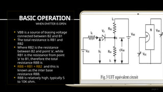
VBB is a source of biasing voltage
connected between B2 and B1
The total resistance is RB1 and
RB2
Where RB2 is the resistance
between B2 and point ‘a', while
RB1 is the resistance from point
‘a' to B1, therefore the total
resistance RBB is
RBB = RB1 + RB2 and this is
known as the inter base
resistance RBB.
RBB is relatively high, typically 5
to 10K ohm.
4.
page 4
BASIC OPERATION
WHENEMITTER IS OPEN
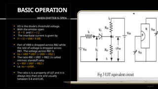
VD is the diode's threshold voltage.
With the emitter open
IE = 0, and I1 = I 2 .
The interbase current is given by
I1 = I2 = VBB / R BB .
Part of VBB is dropped across RB2 while
the rest of voltage is dropped across
RB1. The voltage across RB1 is
Va = VBB * (RB1 ) / (RB1 + RB2 )
The ratio RB1 / (RB1 + RB2 ) is called
intrinsic standoff ratio
ƞ = RB1 / (RB1 + RB2 )
i.e. Va = ƞVBB .
The ratio ƞ is a property of UJT and it is
always less than one and usually
between 0.4 and 0.85.
5.
page 5
BASIC OPERATION
WHENEMITTER IS SHORT
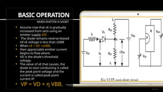
Assume now that vE is gradually
increased from zero using an
emitter supply VEE .
The diode remains reverse biased
till vE voltage is less than ƞVBB
When vE = VD +ƞVBB,
then appreciable emitter current
begins to flow where
VD is the diode's threshold
voltage.
The value of vE that causes, the
diode to start conducting is called
the peak point voltage and the
current is called peak point
current IP.
VP = VD + ƞ VBB.
6.
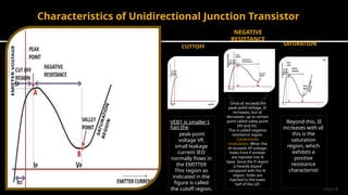
CUTTOFF
VEB1 is smallert
han the
peak-point
voltage VP,
small leakage
current IEO
normally flows in
the EMITTER
This region as
indicated in the
figure is called
the cutoff region.
NEGATIVE
RESISTANCE
Once vE exceeds the
peak point voltage, IE
increases, but vE
decreases. up to certain
point called valley point
(VV and IV).
This is called negative
resistance region.
Conductivity
modulation. When the
vE exceeds VP voltage,
holes from P emitter
are injected into N
base. Since the P region
is heavily doped
compared with the N-
region, holes are
injected to the lower
half of the UJT.
SATURATION
Beyond this, IE
increases with vE
this is the
saturation
region, which
exhibits a
positive
resistance
characteristi
page 6
Characteristics of Unidirectional Junction Transistor
7.
Insert or Drag& Drop your Photo
ADVANTAGES
OF UNIDIRECTIONAL TRANSISTOR
It is a Low cost device
It has excellent characteristics
It is a low-power absorbing device
under normal operating conditions
A stable triggering voltage (VP)— a
fixed fraction of applied inter
basevoltage VBB.
A very low value of triggering
current.
A high pulse current capability.
A negative resistance
characteristic.
8.
Insert or Drag& Drop your Photo
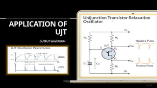
APPLICATIONS
OF UNIDIRECTIONAL TRANSISTOR
They are used in simple oscillators to be built
using just one active device. For example,
they were used for relaxation oscillators
It is used to trigger thyristors (
silicon controlled rectifiers (SCR), TRIAC, etc.).
A DC voltage can be used to control a UJT or
PUT circuit such that the "on-period"
increases with an increase in the DC control
voltage. This application is important for
large AC current control.
UJTs is also used to measure magnetic flux.
UJT applications include sawtoothed
generators, simple oscillators, phase control,
and timing circuits.