The document discusses digital signal processors (DSPs), specifically the TMS320C54xx family of DSPs. It describes the DSPs' architectural features including [1] separate program and data memory buses that allow simultaneous access, [2] a central processing unit with components like a 40-bit ALU and 17x17 multiplier/adder, and [3] on-chip peripherals. It also provides details on the bus structure, central processing unit, and multiplier/adder unit that contribute to the DSPs' high performance for digital signal processing applications.
The document discusses the I2C (Inter-Integrated Circuit) protocol, which is a serial communication standard used to connect low-speed peripherals to embedded systems and other devices. It describes the basic I2C protocol including data transfer methods, components, and modes. It also provides code examples from an iBoot project that implement I2C read and write functionality using registers, state machines, and GPIO interfaces.
#1: The TMS320C54XX DSP uses a modified Harvard architecture with separate program and data buses for high parallelism. It has multiple buses and on-chip memory for efficient data and program flow.
#2: The CPU has a MAC unit, accumulators, ALU, and other components for powerful DSP computing. On-chip peripherals and memory-mapped registers provide efficient I/O.
#3: The architecture utilizes eight buses, on-chip memory blocks, and specialized units like the CSSU to optimize performance of DSP algorithms like Viterbi processing.
- Thumb is a 16-bit instruction set extension to the 32-bit ARM architecture that provides higher code density and smaller memory requirements compared to standard ARM code.
- Thumb instructions are 16-bits wide while ARM instructions are 32-bits wide, allowing Thumb code to be half the size of equivalent ARM code.
- Thumb code executes on ARM processors by decompressing Thumb instructions into their 32-bit ARM equivalents on the processor.
The document provides an overview of the ASIC design and verification process. It discusses the key stages of ASIC design including specification, high-level design, micro design, RTL coding, simulation, synthesis, place and route, and post-silicon validation. It then describes the importance of verification, including why 70% of design time and costs are spent on verification. The verification process uses testbenches, directed and constrained-random testing, and functional coverage to verify the design matches specifications. Verification of more complex designs like FPGAs, SOCs is also discussed.
The 8259 programmable interrupt controller can handle up to 64 interrupts. It supports different operating modes like fully nested, rotating priority, and special mask modes. The 8259's priority structure, vector addresses, masking, and triggering can be programmed. It can generate interrupts in response to either edge or level signals and supports different end of interrupt modes.
BASIC INFORMATION OF ARCHITECTURE OF MICRO-CONTROLLER 8051 AS PER GTU SYLLABUS. Please Comment if u Like.. n Give u r feedback..
For More Information Go to
http://www.noesiseducation.blogspot.com
Advance Microcontroller Bus Architecture(AMBA).
this is a advance bus architecture. it is defined by ARM.
all the content is taken from http://infocenter.arm.com/ website.
The document discusses the 8086 microprocessor. Some key points:
- The 8086 is a 16-bit microprocessor that can access up to 1 MB of memory using a 20-bit address bus. It has 16-bit registers and data bus.
- Internally, it consists of a Bus Interface Unit (BIU) that handles memory access and an Execution Unit (EU) that executes instructions.
- It uses segmentation to divide the 1 MB physical memory into logical segments of 64 KB each for code, data, stack, and extra segments.
- Other features include an instruction queue, multiplexed address/data bus, internal registers, and 40-pin DIP packaging.
8051 micro controllers Instruction set Nitin Ahire
This document discusses the instruction groups of the 8051 microprocessor, including arithmetic, logic, data transfer, boolean, and branching instructions. It provides examples of instructions such as ADD, MOV, ANL, XCH, PUSH, POP, and MOVX. Specific instructions like ADD, SUB, AND, OR, XOR, INC, DEC, SWAP are explained along with examples of their usage. On-chip and off-chip memory access using RD and PSEN signals is also covered.
Functional verification is one of the key bottlenecks in the rapid design of integrated circuits. It is estimated that verification in its entirety accounts for up to 60% of design resources, including duration, computer resources and total personnel. The three primary tools used in logic and functional verification of commercial integrated circuits are simulation (at various levels), emulation at the chip level, and formal verification.
The document discusses the architecture and data addressing modes of the Texas Instruments TMS320C54x digital signal processor (DSP). It describes the DSP's Harvard architecture with separate program and data memory allowing parallel reads and writes. It also outlines the DSP's block diagram including its internal buses, accumulators, barrel shifter, arithmetic logic unit, and multiplier. Finally, it details the various data addressing modes supported by the DSP including immediate, absolute, accumulator, direct, memory-mapped register, stack, and indirect addressing.
This document provides an overview of the 8051 microcontroller architecture. It describes the basic components of the 8051 including 4K bytes of internal ROM, 128 bytes of internal RAM, four 8-bit I/O ports, two timers/counters, one serial interface, and other features. It also discusses the different addressing modes for 8051 assembly language programming including immediate, register, direct, register indirect, and external direct addressing.
The document discusses memory segmentation in the 8086 microprocessor. It explains that the 8086 has a 20-bit address bus that can address 1MB of physical memory. This memory can be divided into 16 segments of 64KB each, addressed from 0000H to F000H. Segments are accessed using a segment register to provide the base address and an offset value. Logical addresses are specified as segment:offset pairs, which are combined and shifted to generate the 20-bit physical address. Segmentation allows code, data, and stacks to be separated and permits relocation of programs in memory.
Microcontroller 8051 and its interfacingAnkur Mahajan
The document discusses microcontrollers and interfacing. It begins with definitions of microprocessors and microcontrollers, comparing their differences. It then focuses on the 8051 microcontroller, describing its features, block diagram, manufacturers, and addressing modes. The document outlines how to write programs for the 8051 and discusses real-world interfacing examples like LCDs, ADCs, relays, motors. It concludes with applications of the 8051 and contact information.
The document introduces dual-port RAM (DPRAM), which is a single static RAM array that can be accessed by two sets of address, data, and control signals simultaneously. This increases bandwidth and offers shorter development times than alternatives. DPRAM uses an 8-transistor cell compared to 6 for regular SRAM, allowing two independent ports to read and write at the same time using different clocks. Applications include cellular base stations, routers, and video conferencing where high-speed concurrent access is needed.
I2c protocol - Inter–Integrated Circuit Communication ProtocolAnkur Soni
This document provides an overview of the I2C communication protocol. It describes how I2C uses only two wires (SDA and SCL) to allow data transmission between an I2C master and multiple I2C slave devices. The document explains the I2C message structure, including the start condition, address frame, read/write bit, data frames, ACK/NACK bits, and stop condition. It also discusses the advantages of I2C, such as supporting multiple masters/slaves and error checking, and disadvantages like slower speeds compared to SPI. Real-life uses of I2C include connections to OLED displays, sensors, and other peripherals.
The document discusses interfacing various peripherals to an 8086 microprocessor using an 8255 PPI chip. It describes the different modes of operation of the 8255 and provides examples of interfacing a keyboard, displays, stepper motor, DAC, and ADC. Circuit diagrams and programming examples are given for displaying numbers on a 7-segment display, generating waveforms using a DAC, and sampling an analog input with an ADC. Interfacing of peripherals like stepper motors, keyboards and displays allows microprocessors to interact with the external world.
The 8086 microprocessor has an architecture that includes a Bus Interface Unit (BIU) and Execution Unit (EU). The BIU fetches instructions and data from memory and computes addresses, while the EU decodes and executes instructions using its 16-bit Arithmetic Logic Unit (ALU). The 8086 has fourteen 16-bit registers for data, addresses, status flags, and pointers that support its operations. It also has an instruction queue that allows the BIU to pre-fetch up to six bytes of upcoming instructions to improve performance.
The memory system of the Intel 80386 microprocessor has the following properties:
- It has a 4GB physical address space that is accessed using virtual addressing via a memory management unit. This allows programs larger than 4GB.
- Memory is divided into four 8-bit wide banks that can each store up to 1GB, allowing the 80386 to transfer 32-bit words in a single cycle.
- There are three types of memory systems used: buffered, pipelined with caches, and interleaved. Buffered systems increase fan-out using buffers. Pipelined systems begin executing instructions before previous ones finish. Interleaved systems improve speed using multiple memory banks.
The instruction set of the 8051 microcontroller is classified into several categories based on the type of operations performed. These include data transfer instructions, byte-level logical instructions, arithmetic instructions, bit-level instructions, rotate and swap instructions, and jump and call instructions. Data transfer instructions move data between registers, memory, and I/O ports using various addressing modes. Byte-level logical instructions perform AND, OR, and XOR operations. Arithmetic instructions support operations like addition, subtraction, multiplication, and division. Bit-level instructions manipulate individual bits in registers and memory. Rotate and swap instructions rotate and rearrange bits and nibbles in the accumulator.
The 8086 microprocessor is Intel's first 16-bit microprocessor released in 1978. It has 20 address lines allowing it to access up to 1 megabyte of memory. It uses segmented memory architecture where the 1 megabyte address space is divided into segments of 64KB each. The 8086 has four 16-bit segment registers - code segment, data segment, stack segment, and extra segment. It operates on minimum and maximum modes determined by the MN/MX pin. In maximum mode, additional pins are used for bus requests and grants.
The document discusses the instruction set of x86 processors. It describes different types of instructions like data transfer, arithmetic, control flow and flag instructions. It provides examples of using MOV, ADD, SUB, CMP and other instructions. It explains concepts like immediate and memory operands, registers, flags, loops and conditional jumps. Key points covered are data transfer using MOV, arithmetic using ADD, SUB, INC, DEC, MUL, DIV, comparison using CMP, and flow control using LOOP, JCXZ and other jump instructions.
The summary provides an overview of the key points about interfacing with the DS1307 real-time clock (RTC) chip using the I2C protocol:
1) The document discusses the I2C protocol signals and components used to interface with the DS1307 RTC, which stores time and date data.
2) It describes initializing the I2C bus, addressing the DS1307 slave device, and transmitting/receiving data to read from and write to the RTC registers.
3) The DS1307 has registers to store seconds, minutes, hours, date, and other time/date fields in BCD format and can output a square wave time signal on its SQW pin at different frequencies.
The document describes the 8086 16-bit microprocessor, including that it has a 20-bit address bus, 16-bit data bus, 29,000 transistors, and supports up to 1MB of memory. It discusses the 8086's architecture, which has a bus interface unit and execution unit, as well as its 14 16-bit registers including general purpose, pointer, index, and segment registers. The document also covers the 8086's instruction queue and concept of segmented memory addressing.
The document summarizes the Intel 80386 microprocessor, which was introduced in 1985. It discusses the key features and architecture of both the 80386DX and 80386SX versions. The 80386 was Intel's first 32-bit microprocessor and supported addressing up to 4GB of physical memory and 64TB of virtual memory using segmentation and paging. It had several operating modes and instruction sets to support multitasking and memory protection in protected mode.
Electronics product design companies in bangaloreAshok Kumar.k
DNCL Technologies Electronic design service and embedded system development ,PCB design, CPLD design & FPGA design and manufacturing service.
DNCL Technologies offers custom electronic design,embedded system design product development and pcb design,FPGA based design & CPLD design,Fireware & device drivers development, RTOS –Vxworks,Kernal programming ,Application Development and android development .
we design all types of electronic circuit or producting according to custom specification at affordable costs while maintaining highest quality product. contact us for your custom electronic product development and manufacturing.
Features of tms_320_2nd_generation_dspSmriti Tikoo
The document describes the features of second generation TMS 320 DSPs, including an 80-ns instruction cycle time, 544 words of on-chip data RAM, a 32-bit ALU/accumulator, a 16x16-bit multiplier, various addressing modes, and support for multiprocessing configurations. Key features are a modified Harvard architecture, single-cycle multiply/accumulate instructions, and flexibility in interfacing with external memory and I/O devices.
The document discusses the features and architecture of the Texas Instruments TMS320C54xx digital signal processor (DSP). It describes the DSP's program sequencer, parallelism and pipelining capabilities, external interfacing features including interrupts and DMA, and its programmable and data memory spaces. The central processing unit contains a 40-bit ALU, two 40-bit accumulators, a barrel shifter, and other components. The DSP has an efficient instruction set and parallel operations that make it well-suited for high-speed signal processing algorithms.
The document discusses the architecture of the TMS320C50 digital signal processor. It describes the TMS320C50's key components including its central processing unit with arithmetic logic unit, parallel logic unit, auxiliary register arithmetic unit, and memory mapped registers. It also outlines the processor's bus structure, on-chip memory including RAM and ROM, and on-chip peripherals such as timers, I/O ports, and serial interfaces. The TMS320C50 uses a Harvard architecture with separate program and data buses for high parallelism and is optimized for digital signal processing applications with features like a single-cycle multiply-accumulate instruction.
Ee6403 --unit v -digital signal processorsJeya Bright
The document discusses the architecture of a digital signal processor (DSP). It describes key components like the central processing unit, memory architecture, instruction set, and on-chip peripherals. The CPU contains an ALU, accumulators, barrel shifter, multiplier, and other functional units. It uses a Harvard architecture with separate program and data memories and multiple buses. Pipelining allows overlapping of instruction execution. On-chip peripherals include timers, serial ports, and a DMA controller.
The document provides an overview of the architecture and features of the TMS320C6713 digital signal processor. It describes the central processing unit, internal memory, general purpose register files, functional units, and peripheral options. The document is a user manual that contains multiple chapters, with each chapter providing examples and explanations of different aspects of the C6713 architecture and software development for the processor.
The document discusses the TMS320C5X digital signal processor. It describes the TMS320 family of DSPs which includes both fixed-point and floating-point processors, with the C5X being a fixed-point processor. The C5X architecture includes a central arithmetic logic unit, parallel logic unit, auxiliary register arithmetic unit, memory-mapped registers and program controller. It has features like on-chip memory and peripherals that enhance performance.
The document provides an introduction to the TMS320F2812 digital signal controller. It begins with definitions of common computing terms like microprocessor, microcontroller, digital signal processor, and digital signal controller. It then compares these terms. The document discusses the architecture of microprocessors, microcontrollers, and digital signal processors. It provides details on the features and architecture of the TMS320F2812, including its CPU, memory, peripherals, math units, and internal bus structure. It describes how the TMS320F2812 combines the processing power of a digital signal processor with memory and peripherals on a single chip.
The document provides an overview of the TMS320C6x architecture. It describes the TMS320C6x as a 32-bit VLIW digital signal processor introduced by Texas Instruments. Key features include its ability to execute up to 8 instructions per cycle and support for floating point operations. The architecture includes 8 functional units, internal memory, external memory interfaces, and peripherals like EDMA controllers and timers. The TMS320C6x is well suited for applications involving real-time signal processing like image and speech processing.
The document provides details about the 80386 processor architecture in real mode. It discusses the 80386 features, architecture, register set, memory addressing, and segmentation in real mode. The architecture of 80386 consists of the central processing unit, memory management unit, and bus interface unit. The central processing unit contains the instruction decoder and execution unit. The execution unit performs operations using the data unit, control unit, and test protection unit.
This presentation is about the design and function of a microprocessor, how to program and how to interface it with other electronics machines and devices
digital signal processing
Computer Architectures for signal processing
Harvard Architecture, Pipelining, Multiplier
Accumulator, Special Instructions for DSP, extended
Parallelism,General Purpose DSP Processors,
Implementation of DSP Algorithms for var
ious operations,Special purpose DSP
Hardware,Hardware Digital filters and FFT processors,
Case study and overview of TMS320
series processor, ADSP 21XX processor
This document describes the creation of an audio mixing environment using Max/MSP. It discusses various mixing console functions like faders, panners, mute/solo buttons, and metering that are implemented in Max/MSP. It explains how fader and panner linking is achieved using a master/slave relationship between controls. Fader automation is also enabled. The document provides details on techniques for panning, metering, equalization and other typical mixing functions.
Microprocessors are computer components made from transistors on a single chip that serve as the central processing unit (CPU) of computers. Microcontrollers are specialized microprocessors designed to control electronic devices. The key differences are that microcontrollers incorporate additional features like RAM, ROM, I/O ports directly on the chip to be self-sufficient, whereas microprocessors rely on external components. An 80286 microprocessor has features like a 16-bit data bus, 24-bit address bus, and memory management abilities. It was used in early PCs and can address up to 16MB of RAM. Microcontrollers are commonly found in embedded systems like appliances and control specific tasks without changes throughout their lifetime.
The document provides an overview of the 80x86 family of microprocessors and assembly programming. It discusses:
1) The evolution of the 80x86 family from the 8080/8085 to the 8086, 8088, 80286, 80386, and 80486, with increasing memory capacity, bus widths, and number of transistors over time.
2) How pipelining allowed the 8086 CPU to fetch and execute instructions simultaneously, improving performance over non-pipelined predecessors.
3) The registers of the 8086, including general purpose, pointer, index, segment, instruction pointer, and flag registers used for different functions.
4) An introduction to assembly programming using MOV
The document provides information on various DSP companies and their products. It discusses Analog Devices' ADSP-218xN and EZ-KIT Lite evaluation boards, as well as its ADSP-2191, ADSP-21535, ADSP-BF561, ADSP 21mod980, ADSP-TS201/202/203, and ADSP-TS201S processors. It also summarizes Texas Instruments' OMAP1510 application processor and TMS320C54CST client-side telephony DSP, among other TI products. Hitachi Semiconductor of America's SH7727 microprocessor is also mentioned. The document concludes with information on DSP products from various other companies.
The document discusses the basic internal structure and operation of a microprocessor. It describes the main components including the arithmetic logic unit (ALU), control unit, register set, accumulator, condition code register, program counter, stack pointer, and bus systems. The control unit coordinates the other components to execute instructions. The ALU performs arithmetic and logical operations on data from the registers and memory. Example microprocessors discussed include the Intel 8085 and MIPS.
x86-64 is a superset of the x86 instruction set architecture. x86-64 processors can run existing 32-bit or 16-bit x86 programs at full speed, but also support new programs written with a 64-bit address space and other additional capabilities.
Removing Uninteresting Bytes in Software FuzzingAftab Hussain
Imagine a world where software fuzzing, the process of mutating bytes in test seeds to uncover hidden and erroneous program behaviors, becomes faster and more effective. A lot depends on the initial seeds, which can significantly dictate the trajectory of a fuzzing campaign, particularly in terms of how long it takes to uncover interesting behaviour in your code. We introduce DIAR, a technique designed to speedup fuzzing campaigns by pinpointing and eliminating those uninteresting bytes in the seeds. Picture this: instead of wasting valuable resources on meaningless mutations in large, bloated seeds, DIAR removes the unnecessary bytes, streamlining the entire process.
In this work, we equipped AFL, a popular fuzzer, with DIAR and examined two critical Linux libraries -- Libxml's xmllint, a tool for parsing xml documents, and Binutil's readelf, an essential debugging and security analysis command-line tool used to display detailed information about ELF (Executable and Linkable Format). Our preliminary results show that AFL+DIAR does not only discover new paths more quickly but also achieves higher coverage overall. This work thus showcases how starting with lean and optimized seeds can lead to faster, more comprehensive fuzzing campaigns -- and DIAR helps you find such seeds.
- These are slides of the talk given at IEEE International Conference on Software Testing Verification and Validation Workshop, ICSTW 2022.
Infrastructure Challenges in Scaling RAG with Custom AI modelsZilliz
Building Retrieval-Augmented Generation (RAG) systems with open-source and custom AI models is a complex task. This talk explores the challenges in productionizing RAG systems, including retrieval performance, response synthesis, and evaluation. We’ll discuss how to leverage open-source models like text embeddings, language models, and custom fine-tuned models to enhance RAG performance. Additionally, we’ll cover how BentoML can help orchestrate and scale these AI components efficiently, ensuring seamless deployment and management of RAG systems in the cloud.
AI 101: An Introduction to the Basics and Impact of Artificial IntelligenceIndexBug
Imagine a world where machines not only perform tasks but also learn, adapt, and make decisions. This is the promise of Artificial Intelligence (AI), a technology that's not just enhancing our lives but revolutionizing entire industries.
Cosa hanno in comune un mattoncino Lego e la backdoor XZ?Speck&Tech
ABSTRACT: A prima vista, un mattoncino Lego e la backdoor XZ potrebbero avere in comune il fatto di essere entrambi blocchi di costruzione, o dipendenze di progetti creativi e software. La realtà è che un mattoncino Lego e il caso della backdoor XZ hanno molto di più di tutto ciò in comune.
Partecipate alla presentazione per immergervi in una storia di interoperabilità, standard e formati aperti, per poi discutere del ruolo importante che i contributori hanno in una comunità open source sostenibile.
BIO: Sostenitrice del software libero e dei formati standard e aperti. È stata un membro attivo dei progetti Fedora e openSUSE e ha co-fondato l'Associazione LibreItalia dove è stata coinvolta in diversi eventi, migrazioni e formazione relativi a LibreOffice. In precedenza ha lavorato a migrazioni e corsi di formazione su LibreOffice per diverse amministrazioni pubbliche e privati. Da gennaio 2020 lavora in SUSE come Software Release Engineer per Uyuni e SUSE Manager e quando non segue la sua passione per i computer e per Geeko coltiva la sua curiosità per l'astronomia (da cui deriva il suo nickname deneb_alpha).
In his public lecture, Christian Timmerer provides insights into the fascinating history of video streaming, starting from its humble beginnings before YouTube to the groundbreaking technologies that now dominate platforms like Netflix and ORF ON. Timmerer also presents provocative contributions of his own that have significantly influenced the industry. He concludes by looking at future challenges and invites the audience to join in a discussion.
Threats to mobile devices are more prevalent and increasing in scope and complexity. Users of mobile devices desire to take full advantage of the features
available on those devices, but many of the features provide convenience and capability but sacrifice security. This best practices guide outlines steps the users can take to better protect personal devices and information.
Maruthi Prithivirajan, Head of ASEAN & IN Solution Architecture, Neo4j
Get an inside look at the latest Neo4j innovations that enable relationship-driven intelligence at scale. Learn more about the newest cloud integrations and product enhancements that make Neo4j an essential choice for developers building apps with interconnected data and generative AI.
HCL Notes and Domino License Cost Reduction in the World of DLAUpanagenda
Webinar Recording: https://www.panagenda.com/webinars/hcl-notes-and-domino-license-cost-reduction-in-the-world-of-dlau/
The introduction of DLAU and the CCB & CCX licensing model caused quite a stir in the HCL community. As a Notes and Domino customer, you may have faced challenges with unexpected user counts and license costs. You probably have questions on how this new licensing approach works and how to benefit from it. Most importantly, you likely have budget constraints and want to save money where possible. Don’t worry, we can help with all of this!
We’ll show you how to fix common misconfigurations that cause higher-than-expected user counts, and how to identify accounts which you can deactivate to save money. There are also frequent patterns that can cause unnecessary cost, like using a person document instead of a mail-in for shared mailboxes. We’ll provide examples and solutions for those as well. And naturally we’ll explain the new licensing model.
Join HCL Ambassador Marc Thomas in this webinar with a special guest appearance from Franz Walder. It will give you the tools and know-how to stay on top of what is going on with Domino licensing. You will be able lower your cost through an optimized configuration and keep it low going forward.
These topics will be covered
- Reducing license cost by finding and fixing misconfigurations and superfluous accounts
- How do CCB and CCX licenses really work?
- Understanding the DLAU tool and how to best utilize it
- Tips for common problem areas, like team mailboxes, functional/test users, etc
- Practical examples and best practices to implement right away
Sudheer Mechineni, Head of Application Frameworks, Standard Chartered Bank
Discover how Standard Chartered Bank harnessed the power of Neo4j to transform complex data access challenges into a dynamic, scalable graph database solution. This keynote will cover their journey from initial adoption to deploying a fully automated, enterprise-grade causal cluster, highlighting key strategies for modelling organisational changes and ensuring robust disaster recovery. Learn how these innovations have not only enhanced Standard Chartered Bank’s data infrastructure but also positioned them as pioneers in the banking sector’s adoption of graph technology.
Observability Concepts EVERY Developer Should Know -- DeveloperWeek Europe.pdfPaige Cruz
Monitoring and observability aren’t traditionally found in software curriculums and many of us cobble this knowledge together from whatever vendor or ecosystem we were first introduced to and whatever is a part of your current company’s observability stack.
While the dev and ops silo continues to crumble….many organizations still relegate monitoring & observability as the purview of ops, infra and SRE teams. This is a mistake - achieving a highly observable system requires collaboration up and down the stack.
I, a former op, would like to extend an invitation to all application developers to join the observability party will share these foundational concepts to build on:
Best 20 SEO Techniques To Improve Website Visibility In SERPPixlogix Infotech
Boost your website's visibility with proven SEO techniques! Our latest blog dives into essential strategies to enhance your online presence, increase traffic, and rank higher on search engines. From keyword optimization to quality content creation, learn how to make your site stand out in the crowded digital landscape. Discover actionable tips and expert insights to elevate your SEO game.
UiPath Test Automation using UiPath Test Suite series, part 5DianaGray10
Welcome to UiPath Test Automation using UiPath Test Suite series part 5. In this session, we will cover CI/CD with devops.
Topics covered:
CI/CD with in UiPath
End-to-end overview of CI/CD pipeline with Azure devops
Speaker:
Lyndsey Byblow, Test Suite Sales Engineer @ UiPath, Inc.
For the full video of this presentation, please visit: https://www.edge-ai-vision.com/2024/06/building-and-scaling-ai-applications-with-the-nx-ai-manager-a-presentation-from-network-optix/
Robin van Emden, Senior Director of Data Science at Network Optix, presents the “Building and Scaling AI Applications with the Nx AI Manager,” tutorial at the May 2024 Embedded Vision Summit.
In this presentation, van Emden covers the basics of scaling edge AI solutions using the Nx tool kit. He emphasizes the process of developing AI models and deploying them globally. He also showcases the conversion of AI models and the creation of effective edge AI pipelines, with a focus on pre-processing, model conversion, selecting the appropriate inference engine for the target hardware and post-processing.
van Emden shows how Nx can simplify the developer’s life and facilitate a rapid transition from concept to production-ready applications.He provides valuable insights into developing scalable and efficient edge AI solutions, with a strong focus on practical implementation.
Unlock the Future of Search with MongoDB Atlas_ Vector Search Unleashed.pdfMalak Abu Hammad
Discover how MongoDB Atlas and vector search technology can revolutionize your application's search capabilities. This comprehensive presentation covers:
* What is Vector Search?
* Importance and benefits of vector search
* Practical use cases across various industries
* Step-by-step implementation guide
* Live demos with code snippets
* Enhancing LLM capabilities with vector search
* Best practices and optimization strategies
Perfect for developers, AI enthusiasts, and tech leaders. Learn how to leverage MongoDB Atlas to deliver highly relevant, context-aware search results, transforming your data retrieval process. Stay ahead in tech innovation and maximize the potential of your applications.
#MongoDB #VectorSearch #AI #SemanticSearch #TechInnovation #DataScience #LLM #MachineLearning #SearchTechnology
GraphRAG for Life Science to increase LLM accuracyTomaz Bratanic
GraphRAG for life science domain, where you retriever information from biomedical knowledge graphs using LLMs to increase the accuracy and performance of generated answers
GraphRAG for Life Science to increase LLM accuracy
Uint3 vtu format
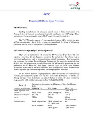
1. UNIT#3
Programmable Digital Signal Processors
3.1 Introduction:
Leading manufacturers of integrated circuits such as Texas Instruments (TI),
Analog devices & Motorola manufacture the digital signal processor (DSP) chips. These
manufacturers have developed a range of DSP chips with varied complexity.
The TMS320 family consists of two types of single chips DSPs: 16-bit fixed point
&32-bit floating-point. These DSPs possess the operational flexibility of high-speed
controllers and the numerical capability of array processors
3.2 Commercial Digital Signal-Processing Devices:
There are several families of commercial DSP devices. Right from the early
eighties, when these devices began to appear in the market, they have been used in
numerous applications, such as communication, control, computers, Instrumentation,
and consumer electronics. The architectural features and the processing power of these
devices have been constantly upgraded based on the advances in technology and the
application needs. However, their basic versions, most of them have Harvard
architecture, a single-cycle hardware multiplier, an address generation unit with dedicated
address registers, special addressing modes, on-chip peripherals interfaces.
Of the various families of programmable DSP devices that are commercially
available, the three most popular ones are those from Texas Instruments, Motorola, and
Analog Devices. Texas Instruments was one of the first to come out with a commercial
programmable DSP with the introduction of its TMS32010 in 1982.
Summary of the Architectural Features of three fixed-Points
Table 3.1
DSPs
Architectural Feature TMS320C25 DSP 56000 ADSP2100
Data representation 16-bit fixed
format 16-bit fixed 24-bit fixed point point
Hardware multiplier 16 x 16 24 x 24 16 x 16
ALU 32 bits 56 bits 40 bits
24-bit program
Internal buses 16-bit program bus 24-bit program bus bus
2 x 24-bit data
16-bit data bus buses 16-bit data bus
24-bit global 16-bit result
2. databus bus
16-bit 24-bit program/data 24-bit program
External buses program/data bus bus bus
16-bit data bus
On-chip Memory 544 words RAM 512 words PROM -
2 x 256 words data
4K words ROM RAM
2 x 256 words data
ROM
64 K words 16K words
Off-chip memory program 64K words program program
64k words data 2 x 64K words data 16K words data
16 words
Cache memory - - program
Instruction cycle time 100 nsec 97.5 nsec. 125 nsecc.
Special addressing
modes Bit reversed Modulo Modulo
Bit reversed Bit reversed
Data address
generators 1 2 2
Synchronous serial
Interfacing features I/O Synchronous and DMA
DMA Asynchronous serial
I/O DMA
3.3. The architecture of TMS320C54xx digital signal processors:
TMS320C54xx processors retain in the basic Harvard architecture of their
predecessor, TMS320C25, but have several additional features, which improve their
performance over it. Figure 3.1 shows a functional block diagram of TMS320C54xx
processors. They have one program and three data memory spaces with separate buses,
which provide simultaneous accesses to program instruction and two data operands and
enables writing of result at the same time. Part of the memory is implemented on-chip
and consists of combinations of ROM, dual-access RAM, and single-access RAM.
Transfers between the memory spaces are also possible.
The central processing unit (CPU) of TMS320C54xx processors consists of a 40-
bit arithmetic logic unit (ALU), two 40-bit accumulators, a barrel shifter, a 17x17
multiplier, a 40-bit adder, data address generation logic (DAGEN) with its own
arithmetic unit, and program address generation logic (PAGEN). These major functional
units are supported by a number of registers and logic in the architecture.
3. A powerful instruction set with a hardware-supported, single-instruction repeat
and block repeat operations, block memory move instructions, instructions that pack two
or three simultaneous reads, and arithmetic instructions with parallel store and load make
these devices very efficient for running high-speed DSP algorithms.
Several peripherals, such as a clock generator, a hardware timer, a wait state
generator, parallel I/O ports, and serial I/O ports, are also provided on-chip. These
peripherals make it convenient to interface the signal processors to the outside world.
In these following sections, we examine in detail the various architectural features
of the TMS320C54xx family of processors.
Figure 3.1.Functional architecture for TMS320C54xx processors.
4. 3.3.1 Bus Structure:
The performance of a processor gets enhanced with the provision of multiple
buses to provide simultaneous access to various parts of memory or peripherals. The
54xx architecture is built around four pairs of 16-bit buses with each pair consisting of an
address bus and a data bus. As shown in Figure 3.1, these are
The program bus pair (PAB, PB); which carries the instruction code from the program
memory.
Three data bus pairs (CAB, CB; DAB, DB; and EAB, EB); which interconnected the
various units within the CPU. In Addition the pair CAB, CB and DAB, DB are used to
read from the data memory, while
The pair EAB, EB; carries the data to be written to the memory. The ‘54xx can generate
up to two data-memory addresses per cycle using the two auxiliary register arithmetic
unit (ARAU0 and ARAU1) in the DAGEN block. This enables accessing two operands
simultaneously.
3.3.2 Central Processing Unit (CPU):
The ‘54xx CPU is common to all the ‘54xx devices. The ’54xx CPU contains a
40-bit arithmetic logic unit (ALU); two 40-bit accumulators (A and B); a barrel shifter; a
17 x 17-bit multiplier; a 40-bit adder; a compare, select and store unit (CSSU); an
exponent encoder(EXP); a data address generation unit (DAGEN); and a program
address generation unit (PAGEN).
The ALU performs 2’s complement arithmetic operations and bit-level Boolean
operations on 16, 32, and 40-bit words. It can also function as two separate 16-bit ALUs
and perform two 16-bit operations simultaneously. Figure 3.2 show the functional
diagram of the ALU of the TMS320C54xx family of devices.
Accumulators A and B; store the output from the ALU or the multiplier/adder
block and provide a second input to the ALU. Each accumulators is divided into three
parts: guards bits (bits 39-32), high-order word (bits-31-16), and low-order word (bits 15-
0), which can be stored and retrieved individually.
Each accumulator is memory-mapped and partitioned. It can be configured as the
destination registers. The guard bits are used as a head margin for computations.
5. AG(39-32) AH(31-16) AL(15-0)
BG(39-32) BH(31-16) BL(15-0)
Figure 3.2.Functional diagram of the central processing unit of the TMS320C54xx
processors.
Barrel shifter: provides the capability to scale the data during an operand read or write.
No overhead is required to implement the shift needed for the scaling operations.
The’54xx barrel shifter can produce a left shift of 0 to 31 bits or a right shift of 0 to 16
bits on the input data. The shift count field of status registers ST1, or in the temporary
register T. Figure 3.3 shows the functional diagram of the barrel shifter of
TMS320C54xx processors.
The barrel shifter and the exponent encoder normalize the values in an
accumulator in a single cycle. The LSBs of the output are filled with0s, and the MSBs
can be either zero filled or sign extended, depending on the state of the sign-extension
6. mode bit in the status register ST1. An additional shift capability enables the processor to
perform numerical scaling, bit extraction, extended arithmetic, and overflow prevention
operations.
Figure 3.3.Functional diagram of the barrel shifter
Multiplier/adder unit: The kernel of the DSP device architecture is multiplier/adder
unit. The multiplier/adder unit of TMS320C54xx devices performs 17 x 17 2’s
complement multiplication with a 40-bit addition effectively in a single instruction cycle.
In addition to the multiplier and adder, the unit consists of control logic for integer and
fractional computations and a 16-bit temporary storage register, T. Figure 3.4 show the
functional diagram of the multiplier/adder unit of TMS320C54xx processors.
The compare, select, and store unit (CSSU) is a hardware unit specifically
incorporated to accelerate the add/compare/select operation. This operation is essential to
implement the Viterbi algorithm used in many signal-processing applications.
The exponent encoder unit supports the EXP instructions, which stores in the T
register the number of leading redundant bits of the accumulator content. This
information is useful while shifting the accumulator content for the purpose of scaling.
7. Figure 3.4. Functional diagram of the multiplier/adder unit of TMS320C54xx processors.
3.3.3 Internal Memory and Memory-Mapped Registers:
The amount and the types of memory of a processor have direct relevance to the
efficiency and performance obtainable in implementations with the processors. The ‘54xx
memory is organized into three individually selectable spaces: program, data, and I/O
spaces. All ‘54xx devices contain both RAM and ROM. RAM can be either dual-access
8. type (DARAM) or single-access type (SARAM). The on-chip RAM for these processors
is organized in pages having 128 word locations on each page.
The ‘54xx processors have a number of CPU registers to support operand
addressing and computations. The CPU registers and peripherals registers are all located
on page 0 of the data memory. Figure 3.5(a) and (b) shows the internal CPU registers and
peripheral registers with their addresses. The processors mode status (PMST) registers
that is used to configure the processor. It is a memory-mapped register located at address
1Dh on page 0 of the RAM.
A part of on-chip ROM may contain a boot loader and look-up tables for function
such as sine, cosine, µ- law, and A- law.
Figure 3.5(a) Internal memory-mapped registers of TMS320C54xx processors.
9. Figure 3.5(b).peripheral registers for the TMS320C54xx processors
Status registers (ST0,ST1):
ST0: Contains the status of flags (OVA, OVB, C, TC) produced by arithmetic operations
& bit manipulations.
ST1: Contain the status of various conditions & modes. Bits of ST0&ST1registers can be
set or clear with the SSBX & RSBX instructions.
10. PMST: Contains memory-setup status & control information.
Status register0 diagram:
ARP TC C OVA OVB DP
(15-13) (12) (11) (10) (9) (8-0)
Figure 3.6(a). ST0 diagram
ARP: Auxiliary register pointer.
TC: Test/control flag.
C: Carry bit.
OVA: Overflow flag for accumulator A.
OVB: Overflow flag for accumulator B.
DP: Data-memory page pointer.
Status register1 diagram:
BRAF(15) CPL XF HM INTM 0 OVM SXM C16 FRCT(6) CMPT(5) ASM
(14) (13) (12) (11) (10) (9) (8) (7) (4-0)
Figure 3.6(b). ST1 diagram
BRAF: Block repeat active flag
BRAF=0, the block repeat is deactivated.
BRAF=1, the block repeat is activated.
CPL: Compiler mode
CPL=0, the relative direct addressing mode using data page pointer is selected.
CPL=1,the relative direct addressing mode using stack pointer is selected.
HM: Hold mode, indicates whether the processor continues internal execution or
acknowledge for external interface.
INTM: Interrupt mode, it globally masks or enables all interrupts.
INTM=0 all unmasked interrupts are enabled.
INTM=1 all masked interrupts are disabled.
0: Always read as 0
OVM: Overflow mode.
OVM=1 the destination accumulator is set either the most positive value or the
most negative value.
OVM=0 the overflowed result is in destination accumulator.
11. SXM: Sign extension mode.
SXM=0 Sign extension is suppressed.
SXM=1 Data is sign extended
C16: Dual 16 bit/double-Precision arithmetic mode.
C16=0 ALU operates in double-Precision arithmetic mode.
C16=1 ALU operates in dual 16-bit arithmetic mode.
FRCT: Fractional mode.
FRCT=1 the multiplier output is left-shifted by 1bit to compensate an extra sign
bit.
CMPT: Compatibility mode.
CMPT=0 ARP is not updated in the indirect addressing mode.
CMPT=1 ARP is updated in the indirect addressing mode.
ASM: Accumulator Shift Mode. 5 bit field, & specifies the Shift value within -16 to 15
range.
Processor Mode Status Register (PMST):
IPTR(15-7) MP/MC(6) OVLY(5) AVIS(4) DROM(3) CLKOFF(2) SMUL(1) SST(0)
Figure 3.6(c).PMST register diagram
INTR: Interrupt vector pointer, point to the 128-word program page where the interrupt
vectors reside.
MP/MC: Microprocessor/Microcomputer mode,
MP/MC=0, the on chip ROM is enabled.
MP/MC=1, the on chip ROM is enabled.
OVLY: RAM OVERLAY, OVLY enables on chip dual access data RAM blocks to be
mapped into program space.
AVIS: It enables/disables the internal program address to be visible at the address pins.
DROM: Data ROM, DROM enables on-chip ROM to be mapped into data space.
CLKOFF: CLOCKOUT off.
SMUL: Saturation on multiplication.
SST: Saturation on store.
12. 3.4 Data Addressing Modes of TMS320C54X Processors:
Data addressing modes provide various ways to access operands to execute instructions
and place results in the memory or the registers. The 54XX devices offer seven basic
addressing modes
1. Immediate addressing.
2. Absolute addressing.
3. Accumulator addressing.
4. Direct addressing.
5. Indirect addressing.
6. Memory mapped addressing
7. Stack addressing.
3.4.1 Immediate addressing:
The instruction contains the specific value of the operand. The operand can be short
(3,5,8 or 9 bit in length) or long (16 bits in length). The instruction syntax for short
operands occupies one memory location,
Example: LD #20, DP.
RPT #0FFFFh.
3.4.2 Absolute Addressing:
The instruction contains a specified address in the operand.
1. Dmad addressing.
MVDK Smem,dmad
MVDM dmad,MMR
2. Pmad addressing.
MVDP Smem,pmad
MVPD pmem,Smad
3. PA addressing.
PORTR PA, Smem,
4.*(lk) addressing .
13. Example:
MVKP 1000h, *AR5 ; 1000 H *AR5 (dmad addressing)
MVPD 1000h, *AR7 ; 1000h *AR7 (pmad addressing)
PORTR 05h, *AR3 ; 05h *AR3 (PA addressing)
LD *(1000h), A ; *(1000h) A (*(lk) addressing)
3.4.3 Accumulator Addressing:
Accumulator content is used as address to transfer data between Program and Data
memory.
Ex: READA *AR2
3.4.4 Direct Addressing:
Base address + 7 bits of value contained in instruction = 16 bit address. A page of 128
locations can be accessed without change in DP or SP.Compiler mode bit (CPL) in ST1
register is used.
If CPL =0 selects DP
CPL = 1 selects SP,
It should be remembered that when SP is used instead of DP, the effective address is
computed by adding the 7-bit offset to SP.
14. Figure 3.7 Block diagram of the direct addressing mode for TMS320C54xx Processors.
3.4.5 Indirect Addressing:
• Data space is accessed by address present in an auxiliary register.
• 54xx have 8, 16 bit auxiliary register (AR0 – AR 7). Two auxiliary register
arithmetic units (ARAU0 & ARAU1)
• Used to access memory location in fixed step size. AR0 register is used for
indexed and bit reverse addressing modes.
• For single – operand addressing
MOD type of indirect addressing
ARF AR used for addressing
• ARP depends on (CMPT) bit in ST1
CMPT = 0, Standard mode, ARP set to zero
CMPT = 1, Compatibility mode, Particularly AR selected by ARP
16. *+AR – 0% Addr = Arx; ARx = circ(ARx - AR0)
*ARx + % Addr = ARx ; ARx = circ (ARx + 1)
Table 3.2 Indirect addressing options with a single data –memory operand.
Circular Addressing;
• Used in convolution, correlation and FIR filters.
• A circular buffer is a sliding window contains most recent data. Circular buffer of
size R must start on a N-bit boundary, where 2N > R .
• The circular buffer size register (BK): specifies the size of circular buffer.
• Effective base address (EFB): By zeroing the N LSBs of a user selected AR
(ARx).
• End of buffer address (EOB) : By repalcing the N LSBs of ARx with the N
LSBs of BK.
If 0 ≤ index + step < BK ; index = index +step;
else if index + step ≥ BK ; index = index + step - BK;
else if index + step < 0; index + step + BK
17. Figure 3.9 Block diagram of the circular addressing mode for TMS320C54xx Processors.
Figure 3.10 circular addressing mode implementation for TMS320C54xx Processors.
18. Bit-Reversed Addressing:
• Used for FFT algorithms.
• AR0 specifies one half of the size of the FFT.
• The value of AR0 = 2N-1: N = integer FFT size = 2N
• AR0 + AR (selected register) = bit reverse addressing.
• The carry bit propagating from left to right.
Dual-Operand Addressing:
Dual data-memory operand addressing is used for instruction that simultaneously
perform two reads (32-bit read) or a single read (16-bit read) and a parallel store (16-bit
store) indicated by two vertical bars, II. These instructions access operands using indirect
addressing mode.
If in an instruction with a parallel store the source operand the destination operand
point to the same location, the source is read before writing to the destination. Only 2 bits
are available in the instruction code for selecting each auxiliary register in this mode.
Thus, just four of the auxiliary registers, AR2-AR5, can be used, The ARAUs together
with these registers, provide capability to access two operands in a single cycle. Figure
3.11 shows how an address is generated using dual data-memory operand addressing.
Name Function
Opcode This field contains the operation code for the instruction
Xmod Defined the type of indirect addressing mode used for accessing the Xmem
operand
XAR Xmem AR selection field defines the AR that contains the address of Xmem
Ymod Defies the type of inderect addressing mode used for accessing the Ymem
operand
Yar Ymem AR selection field defines the AR that contains the address of Ymem
Table 3.3.Function of the different field in dual data memory operand addressing
19. Figure 3.11 Block diagram of the Indirect addressing options with a dual data –memory
operand.
3.4.6. Memory-Mapped Register Addressing:
• Used to modify the memory-mapped registers without affecting the current data-
page pointer (DP) or stack-pointer (SP)
– Overhead for writing to a register is minimal
– Works for direct and indirect addressing
– Scratch –pad RAM located on data PAGE0 can be modified
• STM #x, DIRECT
• STM #tbl, AR1
20. Figure 3.12.16 bit memory mapped register address generation.
3.4.7 Stack Addressing:
• Used to automatically store the program counter during interrupts and
subroutines.
• Can be used to store additional items of context or to pass data values.
• Uses a 16-bit memory-mapped register, the stack pointer (SP).
• PSHD X2
Figure 3.13. Values of stack &SP before and after operation.
Example Problem
1. Assuming the current content of AR3 to be 200h, what will be its contents after
each of the following TMS320C54xx addressing modes is used? Assume that the
contents of AR0 are 20h.
a. *AR3+0
b. *AR3-0
21. c. *AR3+
d. *AR3
e. *AR3
f. *+AR3(40h)
g. *+AR3(-40h)
Solution:
a. AR3 AR3 + AR0;
AR3 = 200h + 20h = 220h
b. AR3 AR3 - AR0;
AR3 = 200h - 20h = 1E0h
c. AR3 AR3 + 1;
AR3 = 200h + 1 = 201h
d. AR3 AR3 - 1;
AR3 = 200h - 1 = 1FFh
e. AR3 is not modified.
AR3 = 200h
f. AR3 AR3 + 40h;
AR3 = 200 + 40h = 240h
g. AR3 AR3 - 40h;
AR3 = 200 - 40h = 1C0h
2. Assume that the register AR3 with contents 1020h is selected as the pointer for
the circular buffer. Let BK = 40h to specify the circular buffer size as
40h.Determine the start and the end addresses fort the buffer. What will be the
contents of register AR3 after the execution to the instruction LD*AR3 + 0%, A,
if the contents of register AR0 are 0025h?
Solution:
AR3 = 1020h means that currently it points to location 1020h. Masking the lower
6 bits zeros gives the start address of the buffer as 1000h. Replacing the same bits
with the BK gives the end address as 1040h.
The Instruction LD*AR3 + 0%, A modifies AR3 by adding AR0 to it and
applying the circular modification. It yields
AR3 = circ(1020h+0025h) = circ(1045h) = 1045h - 40h = 1005h.
Thus the location 1005h is the one pointed to by AR3.
3. Assuming the current contents of AR3 to be 200h, what will be its contents after
each of the following TMS320C54xx addressing modes is used? Assume that the
contents of AR0 are 20h
a. *AR3 + 0B
b. *AR3 – 0B
22. Solution:
a. AR3 AR3 + AR0 with reverse carry propagation;
AR3 = 200h + 20h (with reverse carry propagation) = 220h.
b. AR3 AR3 - AR0 with reverse carry propagation;
AR3 = 200h - 20h (with reverse carry propagation) = 23Fh.
3.5. Memory Space of TMS320C54xx Processors
• A total of 128k words extendable up to 8192k words.
• Total memory includes RAM, ROM, EPROM, EEPROM or Memory mapped
peripherals.
• Data memory: To store data required to run programs & for external memory
mapped registers.
Size 64k words
• Program memory: To store program instructions &tables used in the execution
of programs.
Organized into 128 pages, each of 64k word size
23. Table 3.4.Function of different pin PMST register
PMST bit Logic On-chip memory configuration
MP/MC 0 ROM enabled
1 ROM not available
OVLY 0 RAM in data space
1 RAM in program space
DROM 0 ROM not in data space
1 ROM in data space
24. Figure 3.14 Memory map for the TMS320C5416 Processor.
3.6. Program Control
It contains program counter (PC), the program counter related H/W, hard stack,
repeat counters &status registers.
PC addresses memory in several ways namely:
Branch: The PC is loaded with the immediate value following the
branch instruction
Subroutine call: The PC is loaded with the immediate value
following the call instruction
Interrupt: The PC is loaded with the address of the appropriate
interrupt vector.
25. Instructions such as BACC, CALA, etc ;The PC is loaded with the
contents of the accumulator low word
End of a block repeat loop: The PC is loaded with the contents of the block repeat
program address start register.
Return: The PC is loaded from the top of the stack.