This document describes the design and implementation of a universal shift register (USR) in Verilog. It includes:
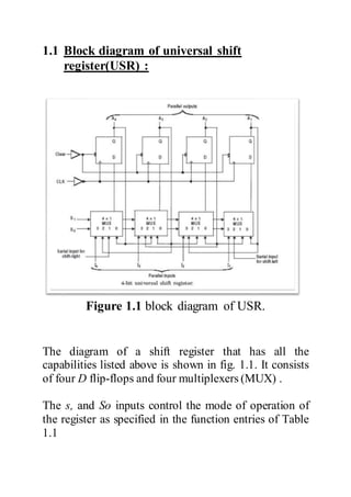
1) A block diagram and description of a USR that can perform shift left, shift right, and parallel load operations using D flip-flops and 4-to-1 multiplexers.
2) The Verilog code for the USR module using D flip-flop and 4-to-1 multiplexer submodules.
3) The test bench and simulation results verifying the USR functionality.

![CHAPTER 2
Implementation of USR in Verilog
2.1 Verilog Code :
`timescale 1ns / 1ps
//modual declaraion of input and output and register
module USR(O,I,clk,reset,s,SINR,SINL);
wire [3:0] w;
input [3:0]I;
input [1:0]s ;
input clk ;
input reset,SINR,SINL;
output [3:0]O;
reg [27:0] count = 0;
//MUX modual calling
mux_4_1 m1(w[0],s[1],s[0],I[0],SINL,O[1],O[0]);
mux_4_1 m2(w[1],s[1],s[0],I[1],O[0],O[2],O[1]);
mux_4_1 m3(w[2],s[1],s[0],I[2],O[1],O[3],O[2]);](https://image.slidesharecdn.com/fc6bb991-cdfd-4ea5-a46c-c6404e2db1e1-161229063353/85/4-bit-uni-shift-reg-4-320.jpg)
![mux_4_1 m4(w[3],s[1],s[0],I[3],O[2],SINR,O[3]);
//D flip flop modual calling
D_FF d1(O[0],w[0],clk,reset);
D_FF d2(O[1],w[1],clk,reset);
D_FF d3(O[2],w[2],clk,reset);
D_FF d4(O[3],w[3],clk,reset);
//increment count on every clock
endmodule
//sub module for D flip flop
module D_FF(q,d,clk,reset);
output reg q;
input d,clk,reset;
always@(posedge clk)
if (reset == 1'b1)
q<=1'b0;
else
q<=d;
endmodule
//sub module for 4x1 MUX
module mux_4_1(y,s1,s0,i3,i2,i1,i0);](https://image.slidesharecdn.com/fc6bb991-cdfd-4ea5-a46c-c6404e2db1e1-161229063353/85/4-bit-uni-shift-reg-5-320.jpg)
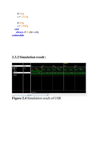
![2.3 Simulationand test bench:
2.3.1 Test bench:
`timescale 1ns / 1ps
module uni_testbench;
// Inputs
reg [3:0] I;
reg clk;
reg reset;
reg [1:0] s;
reg SINR;
reg SINL;
// Outputs
wire [3:0] O;
// Instantiate the Unit Under Test (UUT)
USR uut (
.O(O),
.I(I),
.clk(clk),
.reset(reset),
.s(s),
.SINR(SINR),
.SINL(SINL)
);
initial begin
// Initialize Inputs
//I = 4'b0000;
clk = 1'b1;
reset = 1'b1;
SINR = 1'b1;
SINL = 1'b0;
s = 2'b00;](https://image.slidesharecdn.com/fc6bb991-cdfd-4ea5-a46c-c6404e2db1e1-161229063353/85/4-bit-uni-shift-reg-9-320.jpg)
![Chapter 3
Implementation of CLA on FPGA
Board
3.1 UCF file:
NET "I[0]" LOC = "L13" ;
NET "I[1]" LOC = "L14" ;
NET "I[2]" LOC = "H18" ;
NET "I[3]" LOC = "N17" ;
NET "s[0]" LOC = "H13" | IOSTANDARD = LVTTL | PULLDOWN
| CLOCK_DEDICATED_ROUTE = FALSE;
NET "s[1]" LOC = "K17" | IOSTANDARD = LVTTL | PULLDOWN
| CLOCK_DEDICATED_ROUTE = FALSE;
NET "reset" LOC = "V16"| IOSTANDARD = LVTTL |
PULLDOWN ;
NET "SINL" LOC = "D18"| IOSTANDARD = LVTTL |
PULLDOWN ;](https://image.slidesharecdn.com/fc6bb991-cdfd-4ea5-a46c-c6404e2db1e1-161229063353/85/4-bit-uni-shift-reg-12-320.jpg)
![NET "SINR" LOC = "V4"| IOSTANDARD = LVTTL | PULLDOWN
;
NET "clk" LOC = "C9";
NET "O[0]" LOC = "F12" ;
NET "O[1]" LOC = "E12" ;
NET "O[2]" LOC = "E11" ;
NET "O[3]" LOC = "F11" ;
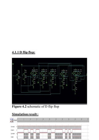
Chapter 4
4.1 Schematic of USR :
Figure 4.1 symbol representation of USR](https://image.slidesharecdn.com/fc6bb991-cdfd-4ea5-a46c-c6404e2db1e1-161229063353/85/4-bit-uni-shift-reg-13-320.jpg)