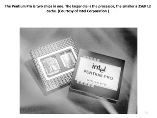
Downloaded 960 times


![When operating with 64 KB of cache, the 386 achieves a hit rate of 93% the processor operates at full speed 93% of the time Instruction set of 386 is 100% compatible with the older processors in the family. 14 new instructions are added and several others are modified. [ex] data can be moved between the internal registers at a time. 80386SX : designed to ease the transition from 16- to 32-bit processors --- 16-bit external data bus and 24-bit address bus . Motaz K. Saad, Dept. of CS](https://image.slidesharecdn.com/x86-1220347983141151-9/85/The-x86-Family-63-320.jpg)
![486DX2 and DX4 DX2 : the internal clock rate is twice the external clock. DX4 : the internal clock rate is three times . Allow to use less expensive components on the computer system board, while the processor operate at its maximum data rate (internally). [Ex] 486DX2 66 : 66 MHz (int. clock) & 33 MHz (ext. clock) 486DX4 100 : 100 MHz (int. clock) & 33 MHz (ext. clock) Overdrive Processors : 486 system boards include an over- drive socket to allow users to upgrade low-speed 486DX or 486SX with 486DX2 and DX4 style processors. Motaz K. Saad, Dept. of CS](https://image.slidesharecdn.com/x86-1220347983141151-9/85/The-x86-Family-65-320.jpg)
![P7 Itanium IA-64 : 7 th -generation processor architecture, Code name = Merced 64-bit architecture : 128 64-bit registers & 128 82-bit floating-point registers (including hidden bits) [c.f.] IA-32 : 10 32-bit reg., 8 fl-pt. reg. Explicit parallelism : instructions are packed in 128-bit bundles ready for execution. Each bundle consists of 3 41-bit instructions and 5-bit template. All three inst- ructions are dispatched in parallel Motaz K. Saad, Dept. of CS](https://image.slidesharecdn.com/x86-1220347983141151-9/85/The-x86-Family-83-320.jpg)
![80x86 Compatible Microprocessors Second Sources : manufacturing 80x86 u-P chips after licensed by Intel. Clones and Look-Alikes Pin-for-pin replacements with all of the same fea- tures as the Intel processor. [Ex] AMD 386DX, 486DX4-100, Cyrix 5x86, etc. Motaz K. Saad, Dept. of CS](https://image.slidesharecdn.com/x86-1220347983141151-9/85/The-x86-Family-85-320.jpg)
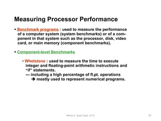
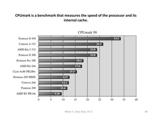
![Dhrystone : a synthetic benchmark consisting of 12 procedures with 94 statements, no fl.-pt. ops. Microprocessor Benchmarks : developed for compa- ring the processing ability of the vaious u-P chips. --- Ziff-Davis ’ CPUmark and Intel ’ s iCOMP index. CPUmark : measures the speed of a PC ’ s proc- essor subsystem, including the CPU, its internal and external caches, and system RAM. [Ex] Fig. 1-20 : CPUmark99 ratings for 80x86s iCOMP : combines 4 industry standard benchmarks : CPUmark32, Norton SI32, SPEC95, and the Intel Media Benchmark (audio, vedio, image, 3-D, etc.). Motaz K. Saad, Dept. of CS](https://image.slidesharecdn.com/x86-1220347983141151-9/85/The-x86-Family-88-320.jpg)
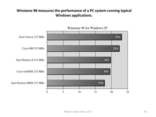
![System-level Benchmarks Microcomputer Benchmarks : measures the speed of processor with considering a slow disk or video subsystem. Winston : System-level, application-based benchmark to measure a PC ’ s overall performance when running today ’ s 32-bit applications on Window 95, 98, NT. [Ex] Winstone 98 ratings for 80x86s Performance Rating : Cyrix and AMD developed the P-rating (Processor Performance) system --- running applications on a processor and compare to a Pentium u-P. [Ex] Table 1-2 : PR166 ~ 366 for AMD and Cyrix chips Motaz K. Saad, Dept. of CS](https://image.slidesharecdn.com/x86-1220347983141151-9/85/The-x86-Family-90-320.jpg)

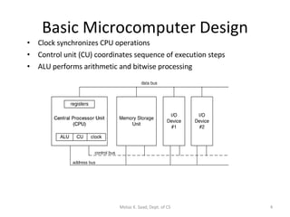
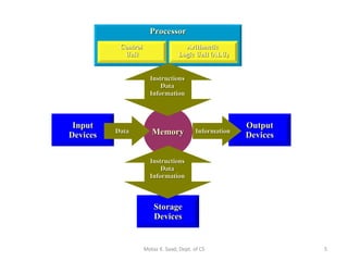
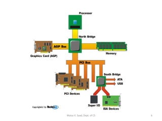
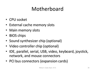
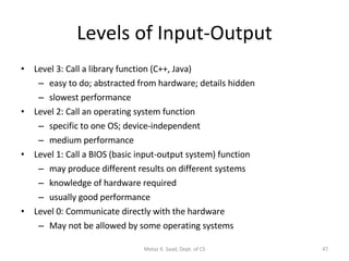
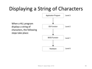
The document provides an overview of x86 assembly language architecture, including: 1) It describes the basic components of an x86 microcomputer including the CPU, memory, input/output ports, and motherboard. 2) It explains x86 processor architecture concepts such as modes of operation, registers, addressing modes, and the evolution of Intel processors. 3) It covers x86 memory management in real mode and protected mode as well as paging and segmentation.


![Chap 02[1]](https://cdn.slidesharecdn.com/ss_thumbnails/chap021-140914002518-phpapp01-thumbnail.jpg?width=640&height=640&fit=bounds)