This proposed work investigates the effects of biasing
circuit in the ultra-wideband microwave low noise amplifier
which operates between 3GHz to 10GHz. The complete circuit is
visualized the importance of every component in the design with
respect to linear measurements like Gain, Noise Figure, Return
loss under unconditionally stable condition. The design and
realization are made by using Hybrid Microwave integrated
circuit in AWR microwave office. The thing that is absolutely
necessary and frequently the difficult step in the design of an
LNA is 'biasing circuit design'. The difficulty situation arises
because traditional methods LNA by using S-parameters data
files in EDA tools provides almost all linear measurements.
Hence a number of time consuming iterations of different biasing
circuits with optimization methods may be required to reach
targeted specifications with the fixed operating point at the
desired points in the load line. Considering this behavior, various
alternate biasing circuit schemes are prepared and founded the
results associated with it. Furthermore, this paper unmistakably
clarifies the impacts of the biasing circuit by utilizing
intermodulation and harmonics distortion technique for
portrayal characterization. Different cases and sorts of the
biasing circuits with various biasing focuses have been tested and given clear perspective of the biasing ideas.
A Study on Protection of Cables by Solkor Differential Protection Relay with ...IJERA Editor
This paper intends to briefly compare the protection of buried three phase high voltage cable with Solkordifferential protection relay using metallic pilot wires orfibre optic pilot wires. Dielectric property of the fiber optic provides complete electrical isolation as well as interference free signaling. This provides total immunity from GPR (ground potential rise), longitudinal induction, and differential mode noise coupling andhigh-voltage hazards to personnel safety. So Fibre optic provides great advantage for Solkor differential protection relaying.
Electrically Controlled Frequency Reconfigurable Comb Type Antenna for Wirele...IDES Editor
Electrically controlled frequency reconfigurable
comb type antenna is presented in this paper. Reconfigurability
is achieved by placing a PIN diode in each slot of the comb
type antenna. The proposed antenna has very compact size
and works on 8 different bands depending upon the state and
number of PIN diode (ON/OFF). Ansoft Designer 7 is used to
simulate the equivalent model for the PIN diode and proposed
antenna is fabricated on FR4 substrate using photolithography
process. As the antenna reconfigure its resonating frequency
from 1st band to 8th band, directivity increases from 3.28 to 4.02
and radiation efficiency increases from 75.3% to 93.45% due
to the improvement in impedance matching at higher band.
Reconfigurable Microstrip Patch Antenna for Frequency Diversity Using RF MEMSIOSR Journals
A novel reconfigurable patch antenna for frequency diversity is proposed by reconfiguring its
geometry using tree rectangular tapes that are connected to the patch via six RF MEMS switches. So switching
between the different frequency bands is achieved by using capacitive series RF-MEMS switches. The antenna
was designed to operate at 2.6 GHz, 3.1 GHz, 3.5 GHz and 5 GHz
International Journal of Engineering Research and Applications (IJERA) is an open access online peer reviewed international journal that publishes research and review articles in the fields of Computer Science, Neural Networks, Electrical Engineering, Software Engineering, Information Technology, Mechanical Engineering, Chemical Engineering, Plastic Engineering, Food Technology, Textile Engineering, Nano Technology & science, Power Electronics, Electronics & Communication Engineering, Computational mathematics, Image processing, Civil Engineering, Structural Engineering, Environmental Engineering, VLSI Testing & Low Power VLSI Design etc.
Design of Reconfigurable Microstrip Patch Antenna for WLAN ApplicationEditor IJMTER
In this paper we propose a rectangular microstrip patch antenna with inset fed which can
operate at 2.4 GHz (IEEE 802.11b) & 5.8 GHz (IEEE 802.11a) WLAN applications. Various slot is
cut into the antenna structure which changes the surface current path resulting in dual resonant
frequency. Further by embedding any switch into a slot, reconfiguration can be achieved i.e. the
antenna can only be used in unlicensed 2.4 GHz band. The achieved directivity is greater than 5db and
the bandwidth obtained is much greater than the required bandwidth. The proposed antenna is
simulated using High Frequency Structure Simulator.
The design & simulation of low noise amplifier for 1 2.8 ghz using aln s...eSAT Journals
Abstract In this paper, we have designed low noise amplifier using 2 stage Cascade topology. We have focused on intermediate matching network design of amplifier for low noise figure and selection of transistor PHEMT is based on noise figure as well as quiescent point required for 0 grid voltage so that amplifier will need only single DC supply i.e. Vdd. Depends upon different topologies used for LNA design with wide band requirement, we chose cascaded topology for good gain with low noise amplifier and optimized for greater bandwidth. Practical inductors are bulky as well as counter intuitive elements for high frequency as they behave as capacitors and to reduce S11. Several windings in inductors make them resistive which increases noise by 0.2-0.4 dB. So we proposed inductor-less input matching network for both stages so that we can increase bandwidth as well as perfect match for low noise figure. This LNA is designed using Advanced Design System (ADS) software to provide 0.5 dB noise figure with power gain of 25 dB and 1-2.5 GHz Bandwidth. So it can be used an L-Band satellite modem that is used in an asset tracking application. Layout is designed using muruta manufacturing lumped components and Aluminum Nitride (AlN) substrate having high dielectric constant and high thermal conductivity. Key Words: LNA, PHEMT, ADS, AlN
Design of Ku-band power divider using Substrate Integrated Waveguide techniquejournalBEEI
A Ku-band Substrate Integrated Waveguide power divider is proposed. In this work, the SIW power divider is designed with T-junction configuration. The SIW technique enables the power divider to have low insertion loss, low cost and features uniplanar circuit. An additional of metallic via hole is added in the center of the junction to improve the return loss performance of the Tjunction SIW power divider. The simulated input return losses at port 1 are better than 27 dB, and features equal power division of about -3.1 dB ±0.4 dB at both output ports across frequency range of 13.5-18 GHz. The SIW power divider is fabricated, and the measurement results show acceptable performances. Since there are some losses contributed by the SMA connector of the fabricated SIW power divider prototype, an additional SIW transmission line is simulated and fabricated to analyze the connector loss.
Numerical parametric study on interval shift variation in simo sstd technique...eSAT Journals
Abstract SSTD (Single Station Time Domain) technique is one of the efficient methods used to extract modal parameters of a structure. Instead of extracting the parameters in frequency domain by utilising Fast Fourier Transform (FFT) as used by some other methods, this technique only relies on free decay responses to obtain the required parameters. In this paper, a parametric study on time shift interval on algorithm method is investigated. The accuracy assessment is made using simulated analytical data with known properties where percentage error between the results of simulated and this method can be calculated and compared. Keywords: SSTD (Single Station Time Domain), FFT, EMA
Design and Implementation of a Low Noise Amplifier for Ultra Wideband Applica...IOSRJVSP
This paper represents the design and implementation of Low Noise Amplifier for Ultra wideband application using 0.18μm CMOS Technology. The proposed two stage LNA is for a 3-5 GHz. At supply voltage of 1.8V, for the exceed limit of 50μm of width of each transistor, the power consumption is 7.22mW. Noise figure is 4.33dB, Maximum power gain i.e. S21 is 20.4dB, S12 < -20dB, S11 < -8dB, S22 < -10dB. For the required bandwidth range, LNA is unconditionally stable and have good linearity
The Influence of Solvent on the Solvolysis of Ethyl Cinnamate in Water Aceton...IJEACS
The kinetic of alkaline hydrolysis of Ethyl Cinnamate was investigated at different percentage of aqua-organic solvent mixture with Acetone (30 to 70% v/v) over the temperature range of 20o C to 40 o C. The specific rate constant was found to be decreased with increasing proportion of solvent (Acetone) at all the temperature range. The Iso-composition Activation energy (EC) was also evaluated which decreases with solvent composition in (water-Acetone) system. The number of water molecule associated with the activated complex is found to be increase (0.7003to 0.786) in water-Acetone system. The Thermodynamic Activation Parameter such as Enthalpy of Activation (H*), Entropy of Activation (S*) and Gibb's free energy of activation (G*) were also calculated
Improved Deadlock Prevention Algorithms in Distributed SystemsIJEACS
Distributed systems deadlock is similar to single-processor system deadlock, but is worse. It is harder to avoid, prevent or detect and is harder to cure, when it is tracked down because all the relevant information is scattered over many machines. In some systems, such as distributed database systems, it can be extremely serious, so it is important to understand how it differs from ordinary deadlock and what can be done about it. Two important deadlock prevention algorithms in distributed systems are wait-die and wound-wait. Their problem is that they just attend to the time stamp of processes, but not priority of them. In a real operating system, attending to priority of processes is very important. The proposed improved algorithms are attending to both priority and time stamp of processes.
International Journal of Engineering Research and Applications (IJERA) is an open access online peer reviewed international journal that publishes research and review articles in the fields of Computer Science, Neural Networks, Electrical Engineering, Software Engineering, Information Technology, Mechanical Engineering, Chemical Engineering, Plastic Engineering, Food Technology, Textile Engineering, Nano Technology & science, Power Electronics, Electronics & Communication Engineering, Computational mathematics, Image processing, Civil Engineering, Structural Engineering, Environmental Engineering, VLSI Testing & Low Power VLSI Design etc.
Six-port Interferometer for W-band Transceivers: Design and CharacterizationIJECEIAES
The study has presented an extensive analysis of an integrated millimeter wave six-port interferometer, operating over a 10 GHz band, from 80 to 90 GHz. It has covered both semi-unlicensed point-to-point links (81-86 GHz), and imaging sensor system frequencies (above 85 GHz). An in-house process is used to fabricate miniaturized hybrid millimeter wave integrated circuits on a very thin ceramic substrate. Two-port S-parameter measurements are performed on a minimum number of circuits integrated on the same die, exploiting the circuit’s physical symmetry and chosen to collect enough data for full-port characterization. Based on these measurements on an integrated prototype, a six-port circuit computer model implemented and advanced system simulations performed for circuit analysis. Interferometer performances evaluated using several methods: analysis of harmonic balance, qi points’, homodyne quadrature demodulation, and error vector modulation (EVM). The analysis showed that this circuit can directly perform, without any calibration, the demodulation of various PSK and QAM signals over the 10 GHz band, with very good results.
A Novel Configuration of a Microstrip Microwave Wideband Power Amplifier for ...TELKOMNIKA JOURNAL
RF/microwave power amplifier (PA) is one of the components that has a large effect on the
overall performance of communication system especially in transmitter system and their design is decided
by the parameters of transistor selected. This letter presents a new concept of a wide-band microwave
amplifier using scattering parameters that is often used in the radio frequency communication systemas an
application of the active integrated antenna[1- 2]. This power amplifier operates from 1.75 GHz to 2.15GHz
frequency and it is based on AT-41410 NPN transistor that has a high transition frequency of 10GHz. The
proposed Single Stage PA is designed by microstrip technology and simulated with Advanced Design
System (ADS) software. The simulation results indicate good performances; the small power gain (S21) is
changed between 11.8 and 10dB. For the input reflection coefficient (S11) is varied between -11 and -
22.5dB. Regarding the output reflection coefficient (S22) is varied between -13.1 and -18.7dB over the
wide frequency band of 1.75-2.15GHz and stability without oscillating over a wide range of frequencies.
BODY ANTENNA WITH DGS FOR BODY CENTRIC WIRELESS COMMUNICATION SYSTEMjantjournal
This paper presents modified patch antenna for 3 GHz and 5 GHz operating frequencies. Here different approaches are studied by varying slot sizes, defected ground size, notch and also changing feed position. Insertion of slots gives dual frequency operation. Notch provides shifting of lower frequency band towards left hand side. Here combined effect of each techniques adopted gives desired result. Proposed antenna resonates for 3 and 5 GHz frequency. Simulation is done using IE3D software for various parameters. Return loss of final design was -12.17 dB for 3 GHz frequency and VSWR of 1.65. For 5 GHz simulation response was -10.04dB return loss and VSWR of 1.91. Proposed antenna is fabricated giving different details. Paper gives good agreement between measured and simulated results.
Design and characterization of frequency reconfigurable honey bee antenna fo...IJECEIAES
In this article, a frequency reconfigurable honey-bee compact microstrip monopole antenna is proposed which is fed by a microstrip line (50 Ω) having the capability of providing dual-band as well as triple-band operation in eight distinct modes. By embedding three PIN diodes overs the honey bee arms, the effective current distribution is controlled hence resonant frequency is also changed in eight distinct modes in real-time. This is the reason the proposed antenna is portrayed as a frequency reconfigurable antenna in this paper which is suitable for cognitive radio application. This proposed antenna can be used for various wireless application such as Bluetooth, Wi-Fi, worldwide interoperability for microwave access (WiMAX), wireless local area network (WLAN), C-band, and X-band applications. The proposed antenna possesses a planner geometry of 39×34×0.87 mm3 which is printed on a substrate as flexible FR-4 (lossy) (εr=4.4 and tanδ=0.019). The proposed antenna exhibits voltage standing wave ratio (VSWR)<2 for all 19 resonant frequencies of interest and perceptible radiation pattern over entire frequency bands with a positive gain. CST microwave studio is used to find out all simulated results of antenna parameters.
Modelling And Miniaturization of A 2-Bits Phase Shifter Using Koch Fractal Sh...IJERA Editor
Phase shifter is a key component in phase array antenna for the Radar application and the wireless communication system. This paper presents a novel design of miniaturised 2bits phase shifter using Koch fractal shapes of one iteration orders. The 3-section branch line coupler is used to extend the bandwidth of the phase shifter,this type of coupler is characterised by a low cost and simplicity of fabrication.Using the Koch fractal geometry the circuit size of the coupler is reduced to 6.36cm ×2.14cm at 2.4GHz. The simulation results show a good performance. So, over 2.1GHz-2.7GHzThe novel design of 2bits fractal reflection phase shifter based on the 3section show a return loss less than -20dB and the phase error varied between 0.1° and 0.4°for the four output phases . The circuit size of the phase shifter is reduced to9.5cm×2.1cm.
Semi-circular compact CPW-fed antenna for ultra-wideband applicationsTELKOMNIKA JOURNAL
This paper presents a simple structure and small size antenna design with dimensions of 43×47 mm2 to perform an ultra-wideband (UWB) frequency range using a semicircular co-planar waveguide (CPW). This antenna has been designed and simulated by the computer simulation technology (CST) microwave studio suit. In this work, we design an ultra-wideband antenna (about 2 GHz to 10 GHz) by feeding a semi-circular compact antenna via a co-planar waveguide for input impedance of 50 Ω. The CST simulation results show that our designed antenna has a very good impedance and radiation characteristic within the intended ultra-wideband. Because of the small size and the suitable shape, this antenna can be used in many wireless communication applications, such as a radio frequency identifier (RFID), indoor wireless local area network or wireless fidelity (WiFi), internet of things (IoT), millimeter waves communications (mmWave), global positioning system (GPS), and many applications of 6G systems.
Negative image amplifier technique for performance enhancement of ultra wideb...IJECEIAES
The paper aims at designing of two stage cascaded ultra-wideband (UWB) low noise amplifier (LNA) by using negative image amplifier technique. The objective of this article is to show the performance improvement using negative image amplifier technique and realization of negative valued lumped elements into microstrip line geometry. The innovative technique to realize the negative lumped elements are carried out by using Richard’s Transformation and transmission line calculation. The AWR microwave office tool is used to obtain characteristics of UWB LNA design with hybrid microwave integrated circuit (HMIC) technology. The 2-stage cascaded LNA design using negative image amplifier technique achieves average gain of 23dB gain and low noise figure of less than 2dB with return loss less than -8dB for UWB 3-10GHz. The Proper bias circuit is extracted using DC characteristics of transistor at biasing point 2V, 20mA and discussed in detail with LNA layout. The negative image matching technique is applied for both input and output matching network. This work will be useful for all low power UWB wireless receiver applications.
Design and Fabrication of S-Band MIC Power Amplifierijcisjournal
In this paper, we demonstrate an approach to design FET (pHEMT) based amplifier. The FET is from
Berex Inc.The design is carried out using the measured S-parameter data of the FET.ADS is used as design
tool for the design. A single-stage power amplifier demonstrated 13dB output gain from 3GHz-4GHz .The
saturated output power of 1W and the power added efficiency (PAE) up to 43%.The amplifier is fabricated
on a selective device GaAs power pHEMT process in MIC (Microwave Integrated Circuit) Technology.
MICs are realized using one or more different forms of transmission lines, all characterized by their ability
to be printed on a dielectric substrate.Active and passive components such as transistors/FET, thin or thick
film chip capacitors and resistors are attached
Similar to The Approach on Influence of Biasing Circuit in Wideband Low Noise Amplifier to Evaluate Robustness Performance (20)
Hybrid optimization of pumped hydro system and solar- Engr. Abdul-Azeez.pdffxintegritypublishin
Advancements in technology unveil a myriad of electrical and electronic breakthroughs geared towards efficiently harnessing limited resources to meet human energy demands. The optimization of hybrid solar PV panels and pumped hydro energy supply systems plays a pivotal role in utilizing natural resources effectively. This initiative not only benefits humanity but also fosters environmental sustainability. The study investigated the design optimization of these hybrid systems, focusing on understanding solar radiation patterns, identifying geographical influences on solar radiation, formulating a mathematical model for system optimization, and determining the optimal configuration of PV panels and pumped hydro storage. Through a comparative analysis approach and eight weeks of data collection, the study addressed key research questions related to solar radiation patterns and optimal system design. The findings highlighted regions with heightened solar radiation levels, showcasing substantial potential for power generation and emphasizing the system's efficiency. Optimizing system design significantly boosted power generation, promoted renewable energy utilization, and enhanced energy storage capacity. The study underscored the benefits of optimizing hybrid solar PV panels and pumped hydro energy supply systems for sustainable energy usage. Optimizing the design of solar PV panels and pumped hydro energy supply systems as examined across diverse climatic conditions in a developing country, not only enhances power generation but also improves the integration of renewable energy sources and boosts energy storage capacities, particularly beneficial for less economically prosperous regions. Additionally, the study provides valuable insights for advancing energy research in economically viable areas. Recommendations included conducting site-specific assessments, utilizing advanced modeling tools, implementing regular maintenance protocols, and enhancing communication among system components.
Cosmetic shop management system project report.pdfKamal Acharya
Buying new cosmetic products is difficult. It can even be scary for those who have sensitive skin and are prone to skin trouble. The information needed to alleviate this problem is on the back of each product, but it's thought to interpret those ingredient lists unless you have a background in chemistry.
Instead of buying and hoping for the best, we can use data science to help us predict which products may be good fits for us. It includes various function programs to do the above mentioned tasks.
Data file handling has been effectively used in the program.
The automated cosmetic shop management system should deal with the automation of general workflow and administration process of the shop. The main processes of the system focus on customer's request where the system is able to search the most appropriate products and deliver it to the customers. It should help the employees to quickly identify the list of cosmetic product that have reached the minimum quantity and also keep a track of expired date for each cosmetic product. It should help the employees to find the rack number in which the product is placed.It is also Faster and more efficient way.
Saudi Arabia stands as a titan in the global energy landscape, renowned for its abundant oil and gas resources. It's the largest exporter of petroleum and holds some of the world's most significant reserves. Let's delve into the top 10 oil and gas projects shaping Saudi Arabia's energy future in 2024.
Vaccine management system project report documentation..pdfKamal Acharya
The Division of Vaccine and Immunization is facing increasing difficulty monitoring vaccines and other commodities distribution once they have been distributed from the national stores. With the introduction of new vaccines, more challenges have been anticipated with this additions posing serious threat to the already over strained vaccine supply chain system in Kenya.
Industrial Training at Shahjalal Fertilizer Company Limited (SFCL)MdTanvirMahtab2
This presentation is about the working procedure of Shahjalal Fertilizer Company Limited (SFCL). A Govt. owned Company of Bangladesh Chemical Industries Corporation under Ministry of Industries.
COLLEGE BUS MANAGEMENT SYSTEM PROJECT REPORT.pdfKamal Acharya
The College Bus Management system is completely developed by Visual Basic .NET Version. The application is connect with most secured database language MS SQL Server. The application is develop by using best combination of front-end and back-end languages. The application is totally design like flat user interface. This flat user interface is more attractive user interface in 2017. The application is gives more important to the system functionality. The application is to manage the student’s details, driver’s details, bus details, bus route details, bus fees details and more. The application has only one unit for admin. The admin can manage the entire application. The admin can login into the application by using username and password of the admin. The application is develop for big and small colleges. It is more user friendly for non-computer person. Even they can easily learn how to manage the application within hours. The application is more secure by the admin. The system will give an effective output for the VB.Net and SQL Server given as input to the system. The compiled java program given as input to the system, after scanning the program will generate different reports. The application generates the report for users. The admin can view and download the report of the data. The application deliver the excel format reports. Because, excel formatted reports is very easy to understand the income and expense of the college bus. This application is mainly develop for windows operating system users. In 2017, 73% of people enterprises are using windows operating system. So the application will easily install for all the windows operating system users. The application-developed size is very low. The application consumes very low space in disk. Therefore, the user can allocate very minimum local disk space for this application.
Democratizing Fuzzing at Scale by Abhishek Aryaabh.arya
Presented at NUS: Fuzzing and Software Security Summer School 2024
This keynote talks about the democratization of fuzzing at scale, highlighting the collaboration between open source communities, academia, and industry to advance the field of fuzzing. It delves into the history of fuzzing, the development of scalable fuzzing platforms, and the empowerment of community-driven research. The talk will further discuss recent advancements leveraging AI/ML and offer insights into the future evolution of the fuzzing landscape.
Forklift Classes Overview by Intella PartsIntella Parts
Discover the different forklift classes and their specific applications. Learn how to choose the right forklift for your needs to ensure safety, efficiency, and compliance in your operations.
For more technical information, visit our website https://intellaparts.com
The Approach on Influence of Biasing Circuit in Wideband Low Noise Amplifier to Evaluate Robustness Performance
1. International Journal of Engineering and Applied Computer Science (IJEACS)
Volume: 02, Issue: 02, February 2017
ISBN: 978-0-9957075-3-5 www.ijeacs.com DOI: 10.24032/IJEACS/0202/03 60
The Approach on Influence of Biasing Circuit in
Wideband Low Noise Amplifier to Evaluate
Robustness Performance
Kishor G Sawarkar 1
, Kushal Tuckley2
Pramod K B 3
, Kumaraswamy H.V 4
1
Research Scholar at MCT’s RGIT
2
Adjunct Professor at IIT, Bombay
1,2
Mumbai, Maharastra, India
3
Ph.D. Student of Jain University
3
Assistant Professor at MCT’s RGIT
4
Department of Telecommunication
4
R. V. College of Engineering, Bangalore, India
Abstract—This proposed work investigates the effects of biasing
circuit in the ultra-wideband microwave low noise amplifier
which operates between 3GHz to 10GHz. The complete circuit is
visualized the importance of every component in the design with
respect to linear measurements like Gain, Noise Figure, Return
loss under unconditionally stable condition. The design and
realization are made by using Hybrid Microwave integrated
circuit in AWR microwave office. The thing that is absolutely
necessary and frequently the difficult step in the design of an
LNA is 'biasing circuit design'. The difficulty situation arises
because traditional methods LNA by using S-parameters data
files in EDA tools provides almost all linear measurements.
Hence a number of time consuming iterations of different biasing
circuits with optimization methods may be required to reach
targeted specifications with the fixed operating point at the
desired points in the load line. Considering this behavior, various
alternate biasing circuit schemes are prepared and founded the
results associated with it. Furthermore, this paper unmistakably
clarifies the impacts of the biasing circuit by utilizing
intermodulation and harmonics distortion technique for
portrayal characterization. Different cases and sorts of the
biasing circuits with various biasing focuses have been tested and
given clear perspective of the biasing ideas.
Keywords- PHEMT, Biasing Networks, AWR microwave office,
Impedance matching, HMIC and LNA
I. INTRODUCTION
Advancing in the wireless communication networks it has
been arise the set of circumstances found that design of
Microwave circuits should meet various parameters at a time
with good performance. In case of LNA the parameters like
Bandwidth, Gain, Noise figure and return loss should all meet
the specifications at the same time eventually all those
parameters with not work with each other favors. To meet at
the specifications with the help of theoretical equations and
majorly the tuners in the commercial software EDA tools like
AWR Microwave office, ADS, HFSS etc. are made quite easier
for microwave circuit designing.
[5] In contrast, hybrid MIC circuits using discrete
components and distributed elements occupy more area and
dissipate more power. However, hybrid MIC technologies
provide a shorter design time, capabilities of customization and
fine tune of fabricated circuits. Also, Optimization of the
variables becomes quite easy.
In this paper, authors present effects of biasing in the LNA
which includes design optimization and analysis of matching
networks and various bias circuits and variation of their effects
in primary circuit are explained. [6] To satisfy high gain, LNA
is designed by using cascade topology and to achieve
maximum power transfer, impedance matching is essential for
proper gain and NF with VSWR. Some of network to build
impedance matching uses lump element, micro strip line or
combination of such elements. Many design of LNA have been
conducted and proposed to satisfy high gain and good
impedances matching network using lump element or micro
strip line and some of characteristic design has been obtained at
the defined frequency and application. For all circuit design the
industrial standard AWR microwave office tool is used, also to
optimize micro strip line and impedance matching to determine
trade off value of gain, Noise Figure, return loss and voltage
standing wave ratio (VSWR).
This paper is organized as follows. The research
background which is composed of recently published articles
with respect to biasing circuits in microwave is described in
Section II, the design of the low-noise amplifier with different
bias circuit is presented in Section III, the LNA performance
under limited set exposures with results are discussed in
Section IV and finally the conclusive remarks are drawn in the
last section.
II. RESEARCH BACKGROUND
This segment examines distributed data about biasing
circuit in microwave circuits, additionally, their estimations
techniques and investigation. [7] In their work, presented a
balun low noise amplifier (LNA) in which the noise figure
(NF) and power consumption are reduced by using a feedback
2. Kishor G Sawarkar et al. International Journal of Engineering and Applied Computer Science (IJEACS)
Volume: 02, Issue: 02, February 2017
ISBN: 978-0-9957075-3-5 www.ijeacs.com DOI: 10.24032/IJEACS/0202/03 61
biasing structure. The circuit was based on a conventional
wideband balun LNA with noise cancellation. In which they
replaced the typical current source of the CG stage by a
transistor that established a feedback loop in that stage. [8]
introduced linearity change of a 10 W GaN HEMT PA utilizing
a dynamic entryway biasing procedure for smoothing an
exchange period of the PA as indicated by the quick
information power. Zhang, Ma, Yu, & Li, [9], exhibited a
dynamic biasing circuit was inserted in the chip which
mitigates the deviation of biasing point, enhances the solidness
and consistency of execution. Both noise and small signal
measurements are performed on-wafer. Ghosh & Srivastava,
[10] , gave the symmetric design biasing system, which makes
the structure polarization uncaring not at all like which was
accounted for active frequency-selective surface(AFSS).
Harzheim, Heuermann, & M. Marso,[11], displayed a versatile
biasing strategy for step recuperation diode based brush
generators which was controlled by a product schedule. The
point was to give the most extreme conceivable consonant
yield power for a given arrangement and diverse information
frequencies amid info power variety.
A. Hypothesis behind the Biasing Circuits
With the thought of practical bias ways for inclination of
transistors. Contrasted with design practice at lower
frequencies, fitting biasing expressions are more constrained
RF and microwave since it is hard to keep the biasing circuit's
parasitic from connecting with the signal path way at
microwave frequencies [12-14].
B. Bias Circuits and its Instabilities
Once the microwave LNA is composed, it stays to give the
dc bias voltages and currents required for the dynamic active
device. This is no straightforward issue, as the courses of action
to present the biases can aggravate the microwave circuit. By
and large, high impedance miniaturized micro strip follows can
be utilized as decoupling inductors, yet alert must be practiced
not to make a low frequency oscillator circuit in the
predisposition bias network system.
A typical reason for inconvenience is the utilization of an
inductor with a huge bypass capacitor, which can make a
resonator in the GHz region that can bolster oscillation of the
active components, which will have high gain at lower
frequencies.
Bias-circuit instabilities are a common source of problems
in amplifiers and other active circuits. These for the most part
result from the utilization of inductors and capacitors in the
Bias-circuit without respect to resonances or circumstances
where 180° stage movement can happen.
III. LNA DESIGN AND ANALYSIS
LNA parameters are mainly depend on S parameters which
varies with respect to frequency. Also Гin depends on Zin and
ГL, ГL depends on ZL and ГIN . Zin and ZL will be different for
different biasing components. Effects of biasing components is
also frequency dependent.
Figure 1. The small signal model of a pHEMT
Cgs and Cgd depends on the biasing voltage because the
depletion region changes with the bias .
Figure 2. The small signal model of a pHEMT at zero drain bias and gate
voltage below pinch-off
The three capacitances Cg, Cs and Cd are given by triangle-
star transformation as given below
Cg = Cgs + Cgd + [(Cgs* Cgd)/ Cds] (1)
Cs = Cgs + Cds + [(Cgs* Cds)/ Cgd] (2)
Cd = Cds + Cgd + [(Cgd* Cds)/ Cgs] (3)
Input port and output port impedances can be expressed
using
Z11 = Rg +Rs + j * [ꙍ( Lg + Ls) – (1/ ꙍ) { ( 1/Cg )+ (1/Cs)}] (4)
Z22 = Rd +Rs + j * [ꙍ( Ld + Ls) – (1/ ꙍ) { ( 1/Cd )+ (1/Cs)}] (5)
Input reflection coefficient and output reflection coefficient
Γin = ( Zin – Z0 )/( Zin + Z0 ) (6)
ΓL = ( ZL – Z0 )/( ZL + Z0 ) (7)
Equivalent input and output impedances can be expressed
in terms of two port Z parameters.
Zin = Z11 – [(Z12* Z21)/( ZL + Z22 )] (8)
ZL = Z22 – [(Z12* Z21)/( ZG + Z11 )] (9)
On the premise of the above arrangement numerical
conditions unmistakably reliance of Γin and ΓL furthermore
Zin and ZL on Cg, Cs and Cd which changes because of
progress in biasing conditions.
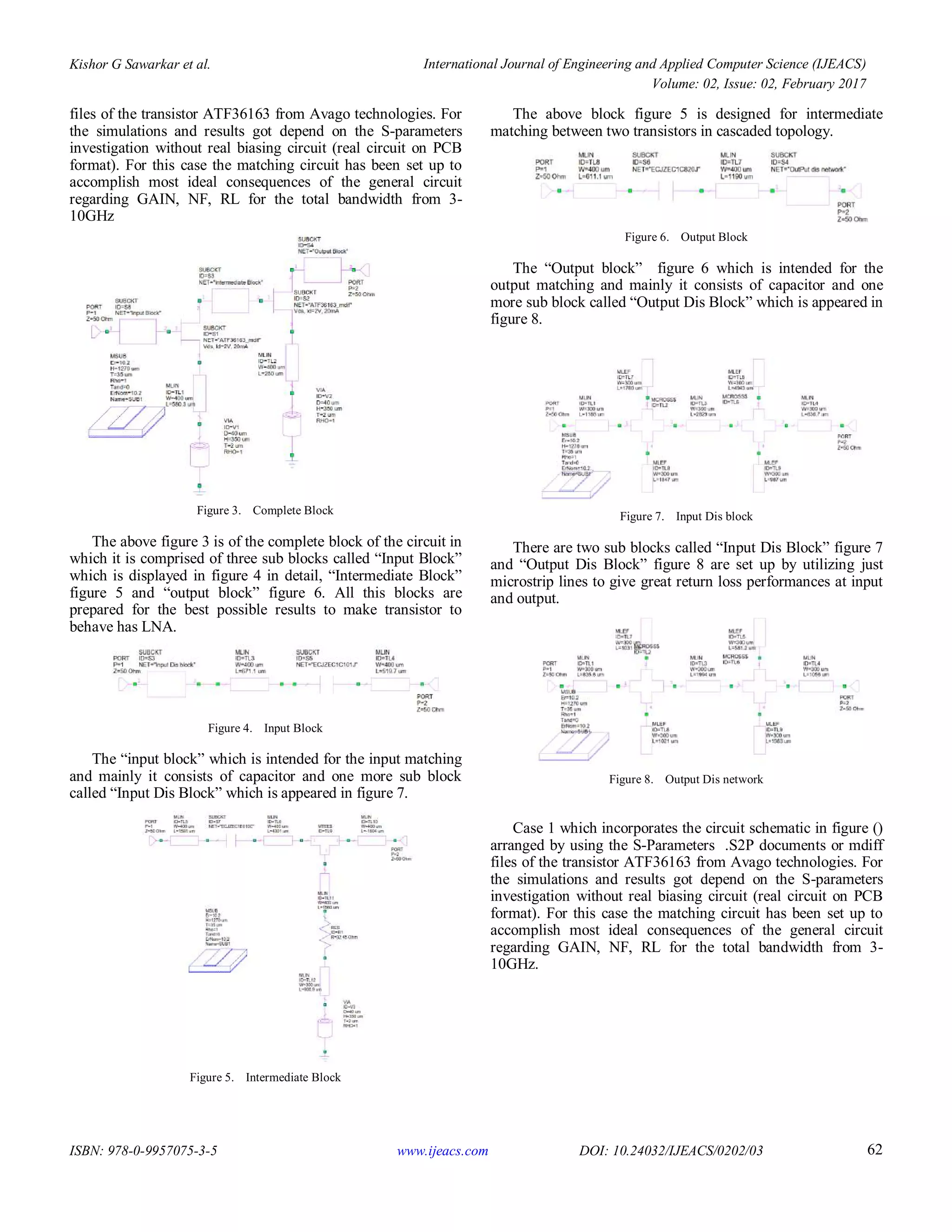
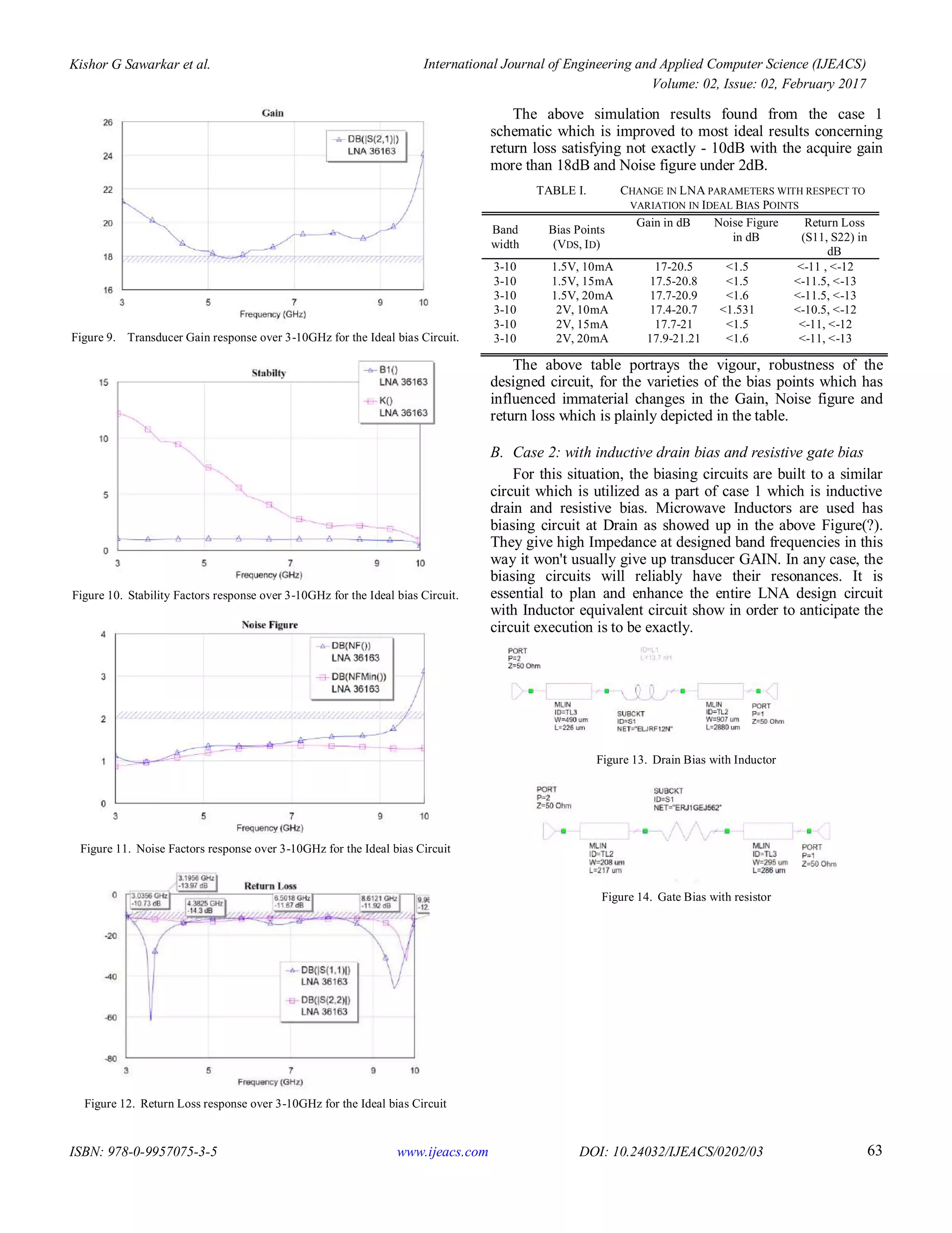
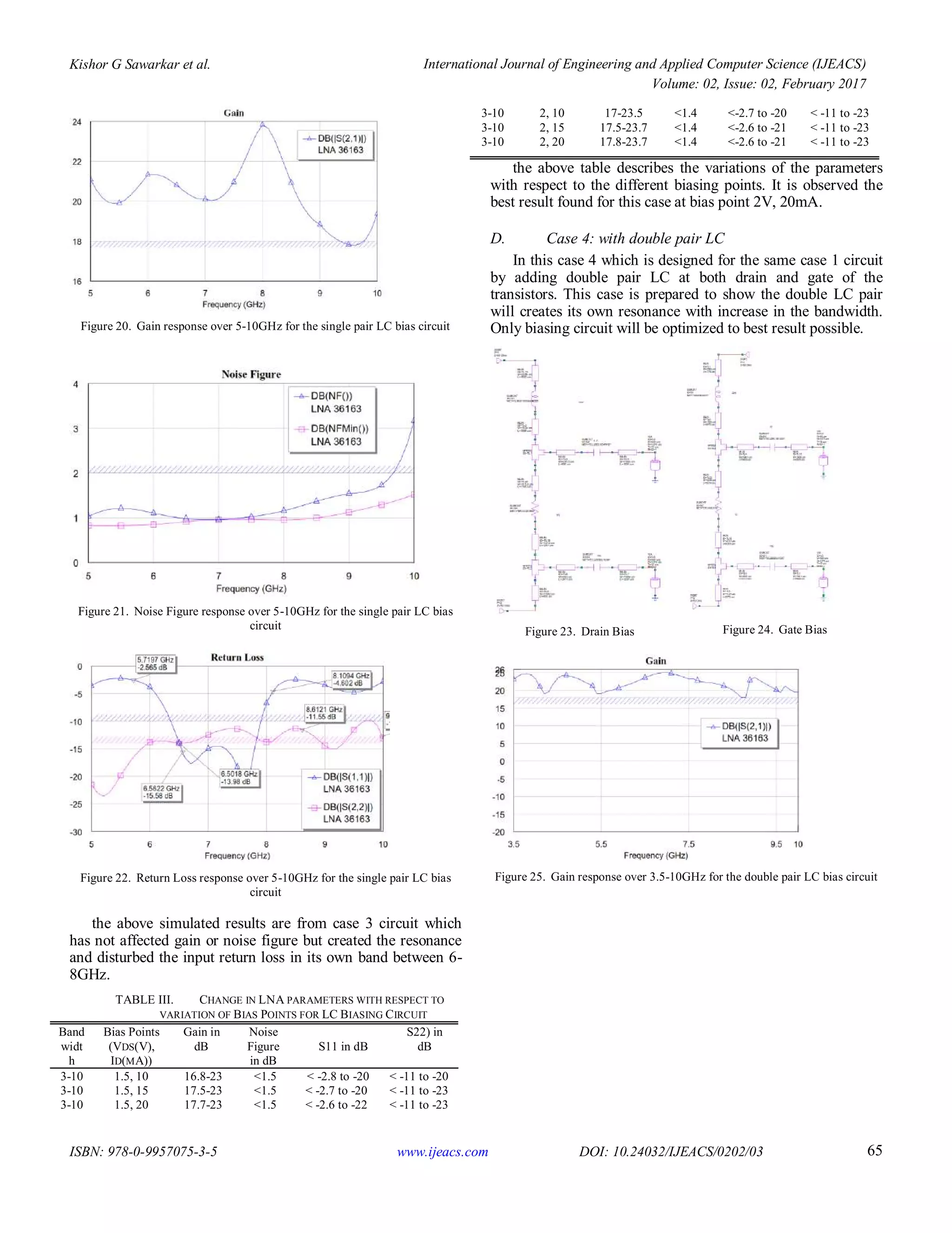
A. Case 1: With Ideal Bias
Case 1 which incorporates the circuit schematic in figure 3
arranged by using the S-Parameters .S2P documents or mdiff
3. Kishor G Sawarkar et al. International Journal of Engineering and Applied Computer Science (IJEACS)
Volume: 02, Issue: 02, February 2017
ISBN: 978-0-9957075-3-5 www.ijeacs.com DOI: 10.24032/IJEACS/0202/03 62
files of the transistor ATF36163 from Avago technologies. For
the simulations and results got depend on the S-parameters
investigation without real biasing circuit (real circuit on PCB
format). For this case the matching circuit has been set up to
accomplish most ideal consequences of the general circuit
regarding GAIN, NF, RL for the total bandwidth from 3-
10GHz
Figure 3. Complete Block
The above figure 3 is of the complete block of the circuit in
which it is comprised of three sub blocks called “Input Block”
which is displayed in figure 4 in detail, “Intermediate Block”
figure 5 and “output block” figure 6. All this blocks are
prepared for the best possible results to make transistor to
behave has LNA.
Figure 4. Input Block
The “input block” which is intended for the input matching
and mainly it consists of capacitor and one more sub block
called “Input Dis Block” which is appeared in figure 7.
Figure 5. Intermediate Block
The above block figure 5 is designed for intermediate
matching between two transistors in cascaded topology.
Figure 6. Output Block
The “Output block” figure 6 which is intended for the
output matching and mainly it consists of capacitor and one
more sub block called “Output Dis Block” which is appeared in
figure 8.
Figure 7. Input Dis block
There are two sub blocks called “Input Dis Block” figure 7
and “Output Dis Block” figure 8 are set up by utilizing just
microstrip lines to give great return loss performances at input
and output.
Figure 8. Output Dis network
Case 1 which incorporates the circuit schematic in figure ()
arranged by using the S-Parameters .S2P documents or mdiff
files of the transistor ATF36163 from Avago technologies. For
the simulations and results got depend on the S-parameters
investigation without real biasing circuit (real circuit on PCB
format). For this case the matching circuit has been set up to
accomplish most ideal consequences of the general circuit
regarding GAIN, NF, RL for the total bandwidth from 3-
10GHz.
4. Kishor G Sawarkar et al. International Journal of Engineering and Applied Computer Science (IJEACS)
Volume: 02, Issue: 02, February 2017
ISBN: 978-0-9957075-3-5 www.ijeacs.com DOI: 10.24032/IJEACS/0202/03 63
Figure 9. Transducer Gain response over 3-10GHz for the Ideal bias Circuit.
Figure 10. Stability Factors response over 3-10GHz for the Ideal bias Circuit.
Figure 11. Noise Factors response over 3-10GHz for the Ideal bias Circuit
Figure 12. Return Loss response over 3-10GHz for the Ideal bias Circuit
The above simulation results found from the case 1
schematic which is improved to most ideal results concerning
return loss satisfying not exactly - 10dB with the acquire gain
more than 18dB and Noise figure under 2dB.
TABLE I. CHANGE IN LNA PARAMETERS WITH RESPECT TO
VARIATION IN IDEAL BIAS POINTS
Band
width
Bias Points
(VDS, ID)
Gain in dB Noise Figure
in dB
Return Loss
(S11, S22) in
dB
3-10 1.5V, 10mA 17-20.5 <1.5 <-11 , <-12
3-10 1.5V, 15mA 17.5-20.8 <1.5 <-11.5, <-13
3-10 1.5V, 20mA 17.7-20.9 <1.6 <-11.5, <-13
3-10 2V, 10mA 17.4-20.7 <1.531 <-10.5, <-12
3-10 2V, 15mA 17.7-21 <1.5 <-11, <-12
3-10 2V, 20mA 17.9-21.21 <1.6 <-11, <-13
The above table portrays the vigour, robustness of the
designed circuit, for the varieties of the bias points which has
influenced immaterial changes in the Gain, Noise figure and
return loss which is plainly depicted in the table.
B. Case 2: with inductive drain bias and resistive gate bias
For this situation, the biasing circuits are built to a similar
circuit which is utilized as a part of case 1 which is inductive
drain and resistive bias. Microwave Inductors are used has
biasing circuit at Drain as showed up in the above Figure(?).
They give high Impedance at designed band frequencies in this
way it won't usually give up transducer GAIN. In any case, the
biasing circuits will reliably have their resonances. It is
essential to plan and enhance the entire LNA design circuit
with Inductor equivalent circuit show in order to anticipate the
circuit execution is to be exactly.
Figure 13. Drain Bias with Inductor
Figure 14. Gate Bias with resistor
5. Kishor G Sawarkar et al. International Journal of Engineering and Applied Computer Science (IJEACS)
Volume: 02, Issue: 02, February 2017
ISBN: 978-0-9957075-3-5 www.ijeacs.com DOI: 10.24032/IJEACS/0202/03 64
Figure 15. Transducer Gain response over 3-10GHz for the inductive drain
bias and resistive gate bias circuit.
Figure 16. Noise Factors response over 3-10GHz for the inductive drain bias
and resistive gate bias circuit.
Figure 17. Return Loss response over 3-10GHz for the inductive drain bias
and resistive gate bias circuit
For the same designed circuit for the case 1, by only
expansion of the inductive drain and resistive gate bias circuit
to has made its own resonance and carried variety of the
outcome as for frequency and obviously appeared in the above
figures.
TABLE II. CHANGE IN LNA PARAMETERS WITH RESPECT TO
VARIATION OF BIAS POINTS FOR INDUCTIVE DRAIN AND RESISTIVE
GATE BIAS
Band
width
Bias Points
(VDS, ID)
Gain in
dB
Noise
Figure
in dB
S11 in dB
S22) in dB
3-10 1.5V, 10mA 15.5-23 <1.5 < (-3 to -15) < (-9 to -20)
3-10 1.5V, 15mA 15.9-23.2 <1.5 < (-3.5to -15.7) < (-9 to -18)
3-10 1.5V, 20mA 16-23.2 <1.6 < (-3.6 to -16) < (-9 to -22.5)
3-10 2V, 10mA 15.5-23.4 <1.5 <(-3.6 to -15) < (-9 to -20)
3-10 2V, 15mA 15.81-23.5 <1.5 <(-3.6 to -16) < (-9 to -21)
3-10 2V, 20mA 15.92-23.62 <1.6 <(-3.7 to -16) < (-9 to -21)
By the insertion of the inductive drain and resistive gate
bias circuit the gain has diminished by 2dB and gain flatness
additionally got aggravated. Because of resistive gate bias
Noise figure got expanded to 2dB and discovered return loss
some enormous variations and it has been found the circuit
bandwidth has decreased to 3-9GHz.
C. Case 3: with single pair LC
In this case, biasing circuit is prepared using a set of
inductor and capacitor at both drain and gate side. Each extra
Inductance with parasitic (resistance, capacitance) in
arrangement with the capacitor grounded, whether of parasitic
source" inside" the capacitor brought about by design or
development, diminishes the adequacy of the bias circuit. The
pair of LC circuits creates its own resonance and disturbs LNA
parameters. Long connections between the capacitor and
ground are extra undesirable arrangement inductance –
regardless of to whether the inductance originates from the
interfacing legs of the capacitor, the conductor tracks or dashes
on the component group installation. Designers and layout
specialists are regularly confronted with apparently practically
insoluble issues in such manner, as limitations, for example, the
space accessibility inside the component group and so on.
Figure 18. Drain Bias Figure 19. Gate Bias
6. Kishor G Sawarkar et al. International Journal of Engineering and Applied Computer Science (IJEACS)
Volume: 02, Issue: 02, February 2017
ISBN: 978-0-9957075-3-5 www.ijeacs.com DOI: 10.24032/IJEACS/0202/03 65
Figure 20. Gain response over 5-10GHz for the single pair LC bias circuit
Figure 21. Noise Figure response over 5-10GHz for the single pair LC bias
circuit
Figure 22. Return Loss response over 5-10GHz for the single pair LC bias
circuit
the above simulated results are from case 3 circuit which
has not affected gain or noise figure but created the resonance
and disturbed the input return loss in its own band between 6-
8GHz.
TABLE III. CHANGE IN LNA PARAMETERS WITH RESPECT TO
VARIATION OF BIAS POINTS FOR LC BIASING CIRCUIT
Band
widt
h
Bias Points
(VDS(V),
ID(MA))
Gain in
dB
Noise
Figure
in dB
S11 in dB
S22) in
dB
3-10 1.5, 10 16.8-23 <1.5 < -2.8 to -20 < -11 to -20
3-10 1.5, 15 17.5-23 <1.5 < -2.7 to -20 < -11 to -23
3-10 1.5, 20 17.7-23 <1.5 < -2.6 to -22 < -11 to -23
3-10 2, 10 17-23.5 <1.4 <-2.7 to -20 < -11 to -23
3-10 2, 15 17.5-23.7 <1.4 <-2.6 to -21 < -11 to -23
3-10 2, 20 17.8-23.7 <1.4 <-2.6 to -21 < -11 to -23
the above table describes the variations of the parameters
with respect to the different biasing points. It is observed the
best result found for this case at bias point 2V, 20mA.
D. Case 4: with double pair LC
In this case 4 which is designed for the same case 1 circuit
by adding double pair LC at both drain and gate of the
transistors. This case is prepared to show the double LC pair
will creates its own resonance with increase in the bandwidth.
Only biasing circuit will be optimized to best result possible.
Figure 23. Drain Bias Figure 24. Gate Bias
Figure 25. Gain response over 3.5-10GHz for the double pair LC bias circuit
7. Kishor G Sawarkar et al. International Journal of Engineering and Applied Computer Science (IJEACS)
Volume: 02, Issue: 02, February 2017
ISBN: 978-0-9957075-3-5 www.ijeacs.com DOI: 10.24032/IJEACS/0202/03 66
Figure 26. Noise Figure response over 3.5-10GHz for the double pair LC bias
circuit
Figure 27. Return Loss response over 3.5-10GHz for the double pair LC bias
circuit
By using double pair LC as biasing circuit has improved
gain and input return loss with minor increase of noise figure.
TABLE IV. CHANGE IN LNA PARAMETERS WITH RESPECT TO
VARIATION OF BIAS POINTS FOR DOUBLE BIASING CIRCUITS
Band
widt
h
Bias Points
(VDS(V),
ID(MA))
Gain in
dB
Noise
Figure
in dB
S11 in dB
S22) in
dB
3-10 1.5, 10 16.8-23 <1.6 < -1.7 to -10 < -9 to -20
3-10 1.5, 15 17.5-23 <1.6 < -1.8 to -10 < -9 to -20
3-10 1.5, 20 17.7-23 <1.6 < -2 to -10 < -9 to -20
3-10 2, 10 17-23.5 <1.6 < -2 to -10 < -9 to -20
3-10 2, 15 17.5-23.7 <1.5 < -2 to -10 < -9 to -20
3-10 2, 20 17.8-23.7 <1.6 < -2 to -10 < -9 to -20
IV. BIASING CIRCUIT EFFECTS ON NON-LINEAR
CHARACTERISTICS
In this section, illustrations and clarifications of LNA
Design Circuit as for biasing Circuit will be given. [15-16] The
effects of Biasing circuit are explained by insertion of single
tone sinusoidal voltage wave (V sin(ωt)) to the non-signal
voltage results in
vgs= VGSQ + V sin(ωt)
vgs will be the function of Vds and Id biasing point of the
transistor which has already been tabulated for the multiple
cases and discussed. Then the harmonic distortion KF is
Where V is maximum amplitude of the signal.
Noted: Distortion Factor approaches to its minimum as
tends to 0
Cross modulation (Intermodulation) produced when two
sine wave signals are amplified at the same time.
vgs= VGSQ + V1 sin(ωt) + V2 sin(ωt) (12)
Since the output current includes the sum and difference
components of the two sinusoidal waves in which
intermodulation results in
√ √
In this case, also it has been clearly examined that distortion
factor decreases as bias is brought closer to =0. These two-
distortion factor will exist in biased circuit which will
deteriorate performance of the designed circuit.
V. SUMMARY
The experimented results of this work can be summarized
as following in the preferences of cases:
Case1: Ideal Bias LNA circuit intended for the best
reasonable estimations of Gain, NF and Bandwidth (3-10GHz)
which is utilized to correlate for the remaining three biasing
strategies likely Drain Inductance and gate resistance bias, LC
bias and double LC bias.
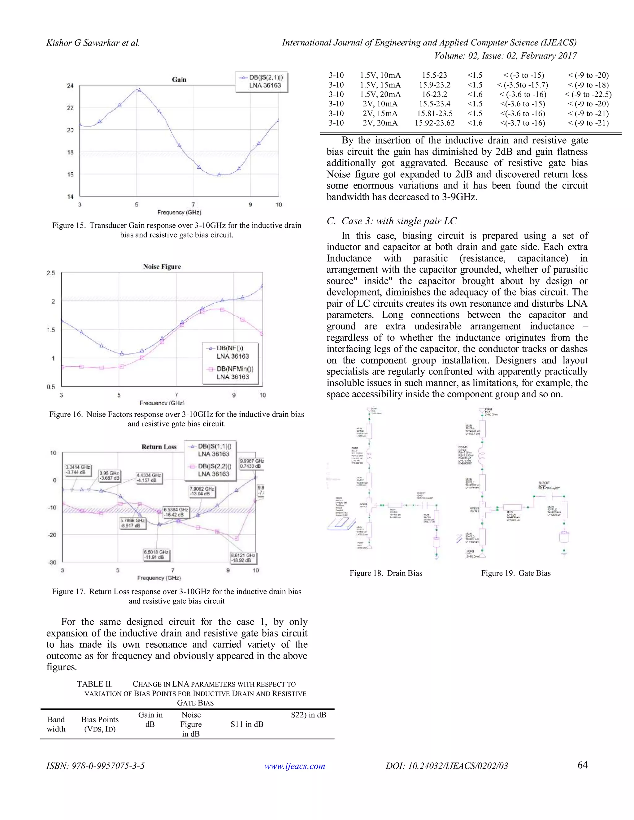
Case 2: Drain Inductance and gate resistance bias is
recommended for the LNA design whose bandwidth is up to
4GHz. The performance in this case linearly Gain decrease
and NF increases and stability will not be affected at any cost.
Case 3: LC bias is suggested for the LNA design for the
smaller bandwidth generally around 2GHz. The LNA
performance with respect to Gain and NF will be great and
results will keep up flatness over small bandwidth.
Case 4: Double LC is proposed for the wideband and ultra-
band with the viable cost on return loss, Gain and NF won't be
highly influenced.
A. Confinement of the Biasing Circuit Design
1) the main cause of the distortion or the variations of the
results with various cases of the biasing circuit is the non-
linearity in the transfer characteristics of the overall circuit with
micro strip line
2) Distortion is also caused by the output conductance gd
related to operating point and drain voltage Vds.