Download to read offline
![International Journal of VLSI design & Communication Systems (VLSICS) Vol.6, No.4, August 2015
DOI : 10.5121/vlsic.2015.6402 15
DESIGN APPROACH FOR FAULT
RECOVERABLE ALU WITH IMPROVED FAULT
TOLERANCE
Ankit K V1
, S Murali Narasimham2
and Dr. Viajya Prakash A M3
1
PG Student, Department of E & C, B.I.T, Bangalore, KA, India
2
Associate Professor, Department of E & C, B.I.T, Bangalore, KA, India
3
Professor, Department of E & C, B.I.T, Bangalore, KA, India
ABSTRACT
A new design for fault tolerant and fault recoverable ALU System has been proposed in this paper.
Reliability is one of the most critical factors that have to be considered during the designing phase of any
IC. In critical applications like Medical equipment & Military applications this reliability factor plays a
very critical role in determining the acceptance of product. Insertion of special modules in the main design
for reliability enhancement will give considerable amount of area & power penalty. So, a novel approach
to this problem is to find ways for reusing the already available components in digital system in efficient
way to implement recoverable methodologies. Triple Modular Redundancy (TMR) has traditionally used
for protecting digital logic from the SEUs (single event upset) by triplicating the critical components of the
system to give fault tolerance to system. ScTMR- Scan chain-based error recovery TMR technique provides
recovery for all internal faults. ScTMR uses a roll-forward approach and employs the scan chain
implemented in the circuits for testability purposes to recover the system to fault-free state. The proposed
design will incorporate a ScTMR controller over TMR system of ALU and will make the system fault
tolerant and fault recoverable. Hence, proposed design will be more efficient & reliable to use in critical
applications, than any other design present till today.
KEYWORDS
Fault recovery, tolerance, ALU, ScTMR, ALU designing, critical applications, scan chains & ScTMR.
1. INTRODUCTION
Today is the era of technological advancement in number of features contain by any system. The
technological trends are moving towards incorporation of more and more functionality inside
small integrated chips. The exponential growth in amount of SOC design coming out in market
further supports this trend. But the primary characteristic property of any device still counts with
Reliability. Accumulation and increment of features cannot overrun the surety requirement a
device have to show to last in the challenging competitive market. A lot of research is going
nowadays in VLSI design domain to make designs more reliable and error resistant.
For all the critical applications, we need to develop techniques which will make a design more
reliable and error resistant. Just testing and verification is not enough to increase the reliability of
the system but design should have inbuilt property to tolerate the fault, if any occurs while the
device is in operation. Moreover, just fault tolerance is not sufficient without incorporating the
fault recovery techniques also inside the design, for making it completely reliable and less error
prone.
Microprocessors are the most critical, important and necessary part of any modern digital systems
and the heart of microprocessor is ALU [1]. If the ALU itself got faulty, the entire device will](https://image.slidesharecdn.com/designapproachforfault-150910093510-lva1-app6892/75/Design-approach-for-fault-1-2048.jpg)
![International Journal of VLSI design & Communication Systems (VLSICS) Vol.6, No.4, August 2015
16
come to halt. Hence, it is a necessity to make ALU to be fault tolerable in all the critical
application where reliability is most critical factor.
In this paper a new design for ALU system is purposed which is not just more fault tolerant but
also have fault recovery mechanism inbuilt inside. This has been designed keeping the size and
area penalty minimum by reusing the already present scan chains in the design, to get fault
recovery.
2. FAULT TOLERANT SYSTEMS
If system able to continue its normal operation even after failing of one or more of its
components, then this property of the system is called fault tolerance. The operating quality is
proportional to the severity of the failure i.e. operating quality decreases as the severity of the
failure increases for naively designed systems [2]. Fault tolerance becomes substantial design
criteria for the applications where the reliability of hardware is crucial. Medical, military and
long-range missions are such applications that the fault tolerance of hardware became key issue.
Fault tolerant systems are such systems wherein even if a certain part of a system fails; it doesn’t
affect the normal operation of that system [3]. The degree of normal operation depends on the
degree or harshness of the fault. In other words the normal operation becomes more and more
critical with the increase of harshness of the fault.
The main and crucial characteristics of a fault tolerant system are:
• The designed system must be intelligent enough to carry on the normal operation for the
duration of the fault, i.e. until it is repaired
• The system must be able to identify the faulty components and isolate them
• All sorts of supplies and connection to the faulty component must be put off, i.e. the
faulty component must be forced to go dead till it is repaired and becomes operational.
The critical components or functions of the system are duplicated or might be triplicated, so as to
increase the reliability of the system. This process is called redundancy.
3. RECOVERY TECHNIQUES
If desired level of operational conditions is re-establish after occurrence of fault in the system
then this phenomenon is called as fault recovery [11]. A system which is capable of recovering
from the fault after error event is said to be fault recoverable system. Fault recovery can be
achieved by many techniques depending upon nature of faults. Few faults are temporary and easy
to recover like transient faults, struck at faults etc. while some are permanent faults and hard to
recover [5]. Scan chains available in design for testability can be used to re-establish the sates of
internal circuitry, and thus recover the fault in system.
Generally there are two famous recovery techniques used in VLSI designs: roll-back recovery and
roll forwards recovery technique. In former the checkpoints are defined in the design and while
executing if a fault occurs, then the system goes back to immediate previous point to loads the
previous saved states into the logic circuitry and start functioning again from that point.
In case of roll forward technique, the states from another fault free module will be loaded into the
faulty module and operation will be resumed from that point itself. This later one is much better
and efficient as saves the time required for re-computation in the former.](https://image.slidesharecdn.com/designapproachforfault-150910093510-lva1-app6892/75/Design-approach-for-fault-2-2048.jpg)
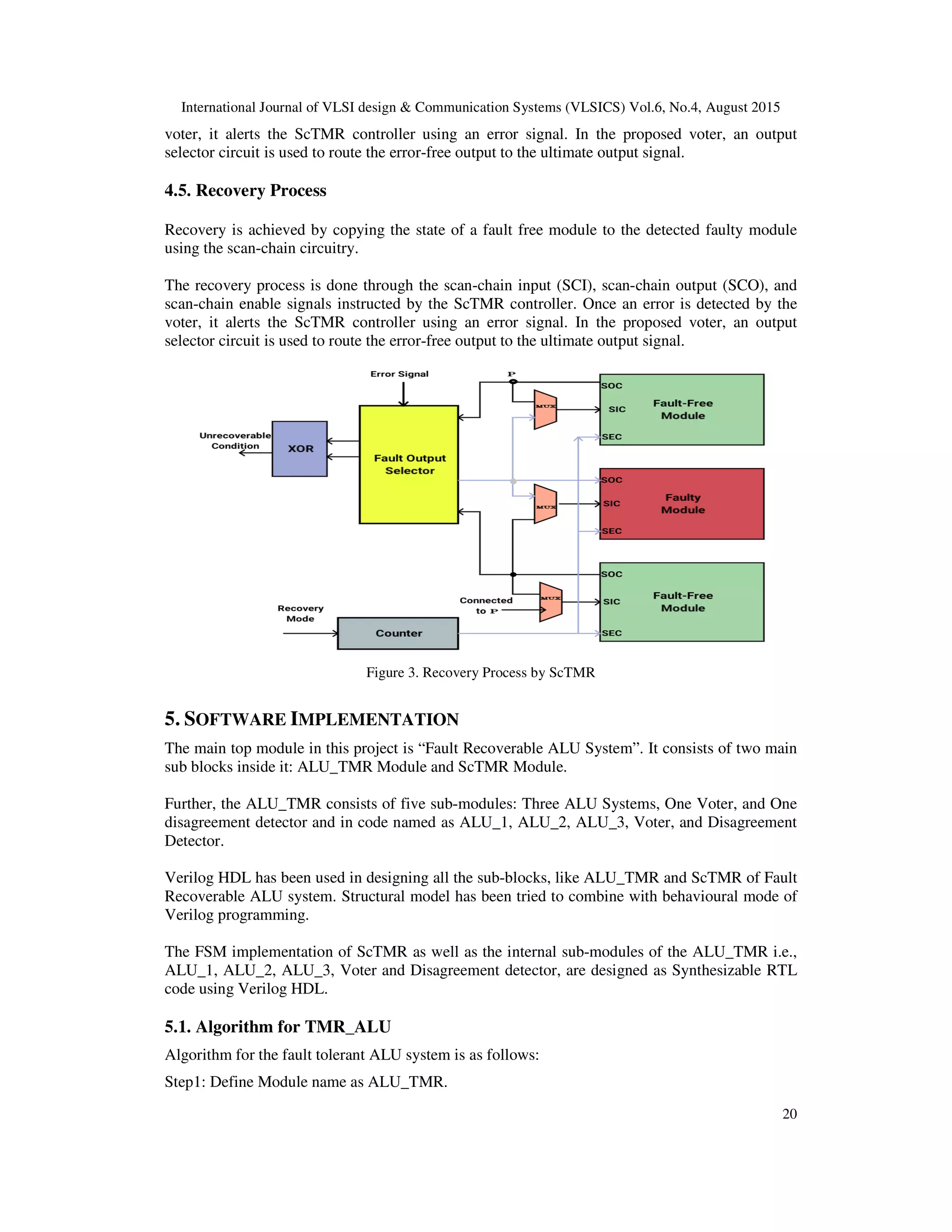
![International Journal of VLSI design & Communication Systems (VLSICS) Vol.6, No.4, August 2015
17
4. PROPOSED DESIGN METHODLOGY
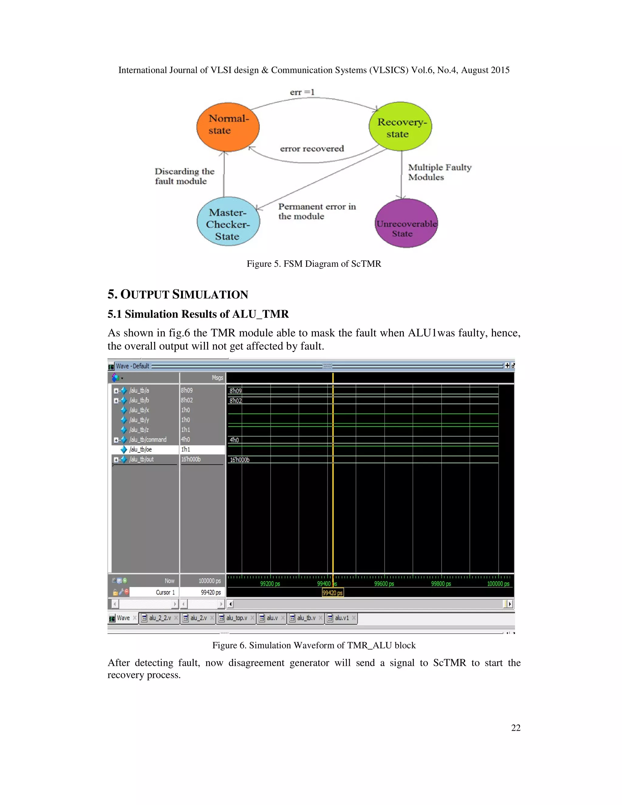
The following section contains all the integral information about the proposed design of Fault
recoverable ALU System with all components and their description with block diagrams.
4.1. Triple Modular Redundancy
It has been known that the reliability of digital systems can be improved through the use of
redundant components, if these additional components are properly employed.
The most common type of redundancy method is Triple Modular Redundancy (TMR). Triple
modular redundancy, (TMR) is a fault-tolerant form of N-modular redundancy, in which three
systems perform a process and that result is processed by a voting system to produce a single
output [6]. If any one of the three systems fails, the other two systems can correct and mask the
fault. If the voter fails then the complete system will fail. The majority voter uses voting logic as
shown in Fig. 1.
Figure 1. Block diagram of voting logic circuit used in designing TMR system
In TMR, all the three inputs are compared by the majority voter circuit and then the final output is
decided upon. Suppose two out of three modules have same outputs then the majority voter
decides which replication has error as two-to-one vote is pragmatic by the majority voter [8].
After this decision is made only two modules are left and the majority voter can switch to dual
modular redundancy (DMR).
TMR can be employed for N number of imitations. The arrangement of redundancies will not fail
if none of the three modules fails, or if just one of the three modules fails. The voting logic
evaluates the output of all the modules and then it passes the majority output i.e. if all three
outputs are equal then it turns out to be the final output and if two out of three outputs are equal
then the two similar outputs turn out to be the final output. Also, if the two equal outputs are
falsified output then it will turn out to be the final output.](https://image.slidesharecdn.com/designapproachforfault-150910093510-lva1-app6892/75/Design-approach-for-fault-3-2048.jpg)
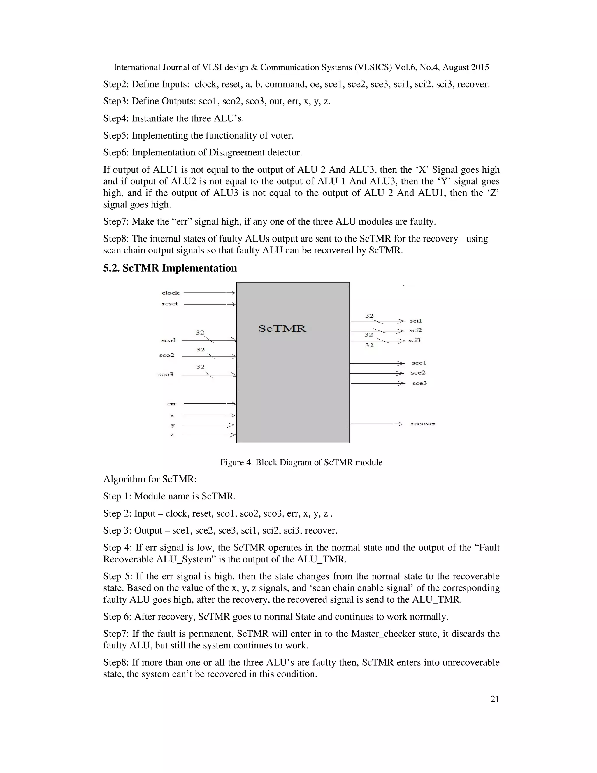
![International Journal of VLSI design & Communication Systems (VLSICS) Vol.6, No.4, August 2015
18
4.2. Proposed ALU Design
Arithmetic Logic Unit (ALU) is the most critical part of any microprocessor or microcontroller. It
is also the heart and soul of any central processing unit (CPU). ALU implements logic operations,
such as AND, NOT, OR etc., and arithmetic operations, such as ADD, SUBTRACT,
MULTIPLICATION etc. [7]. Most ALUs can perform following operations:
a. Bitwise logic operations: - NAND, NOR, XNOR
b. Integer arithmetic operation
c. Bit-shifting operations
The ALU module proposed in this paper have more sequential element to accommodate scan
chains functionally. Pipelining is used to increase the throughput as well as for inclusion of DFT
(design for testability) in design [9]. Generally only adder is used in ALU systems to realize other
arithmetic logic like subtraction and multiplication etc [4]. In our proposed design the adder used
is pipelined RCA (ripple carry adder) because of its compact design [10].
The scan chain has been added in the design by replacing registers with a scan cell named D-mux
Cell. The scan cell works as a large shift registers while testing and for normal operation work as
a simple D-Flip flop [9]. The scan logic is implemented in RTL code and later it will be used for
fault recovery also by inbuilt recovery controller ScTMR.
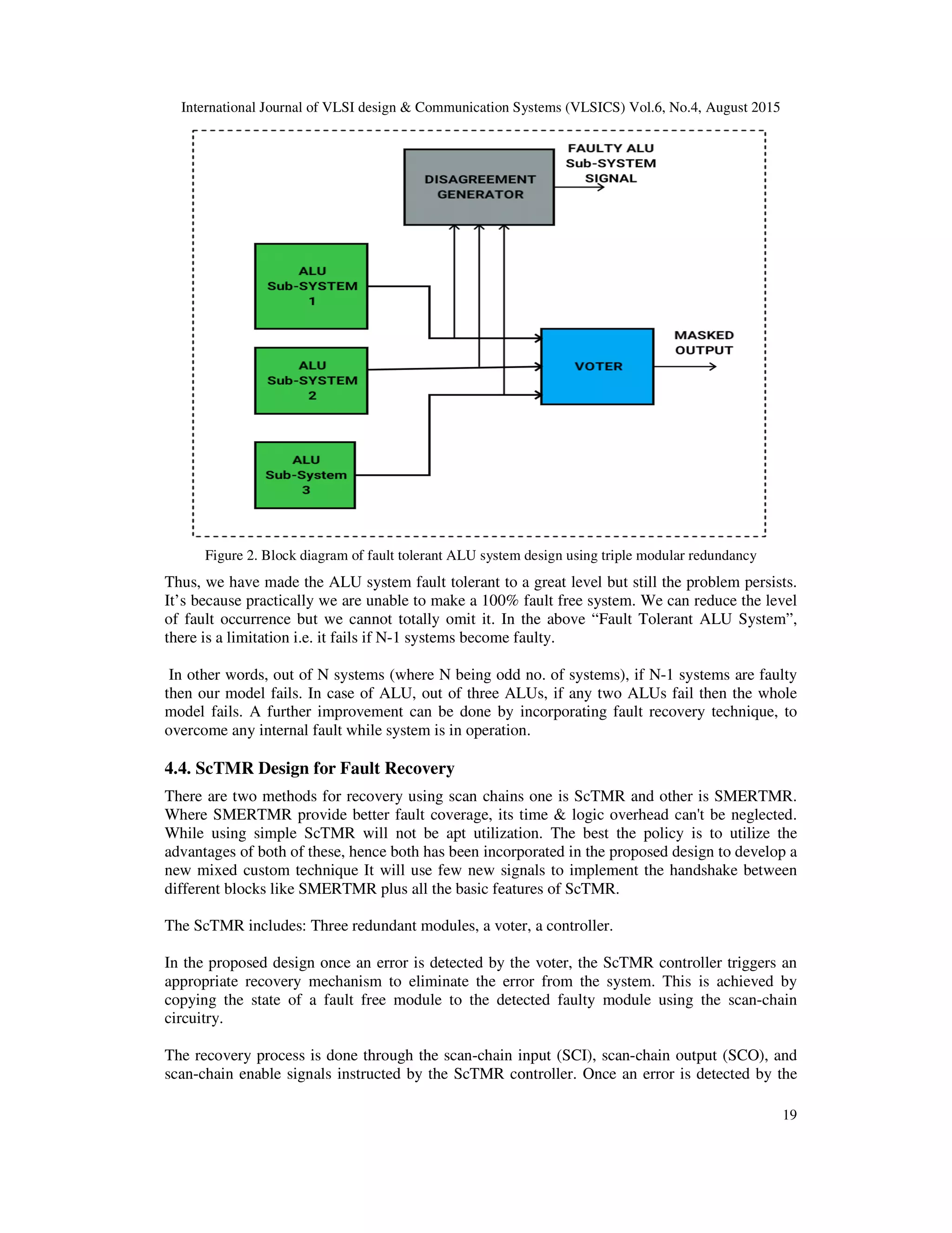
4.3. Fault Tolerant ALU System
Triple modular redundancy has been used in order to design the fault tolerant ALU system. In this
process the ALU system carried out is triplicated, each having the same input, thus making it
triple mode redundant. The output of all the three ALUs is passed onto the Voting Circuit which
contrasts the outputs and then passes the majority output.
It means that if any two ALUs are giving the similar output, then that output will be passed by the
voting circuit and that turns out to be the final output of the entire circuit. In case of all the ALUs
giving the similar outputs, then that output becomes the last output but in case of all the three
ALUs giving dissimilar outputs then the voting circuit faces a dilemma and it fails. At this time
the final output is undefined.](https://image.slidesharecdn.com/designapproachforfault-150910093510-lva1-app6892/75/Design-approach-for-fault-4-2048.jpg)
![International Journal of VLSI design & Communication Systems (VLSICS) Vol.6, No.4, August 2015
24
• The penalty of Area and power requirement of the system is just nearly 21-23 per cent,
but the reliability has been increased by 9 folds, making this system apt for critical
medical and defence application use.
ACKNOWLEDGEMENTS
The author would like to thank everyone who has influenced the proposed work, especially Dr.
KV Prasad, HOD, Dept. of E&C, BIT. Special acknowledgments to my colleagues Ms S. S and
Mr Raj.
REFERENCES
[1] Rakshith Saligram, Shrihari Shridhar Hegde, Shashidhar A Kulkarni, H.R.Bhagyalakshmi and M.K.
Venkatesha, (2013) “Design Of Parity Preserving Logic Based Fault Tolerant Reversible Arithmetic
Logic Unit”, International Journal of VLSI Design & Communication Systems (VLSICS), Vol.4,
No.3.
[2] Meshram, M. S. S., and Belorkar, M. U. A., (2011) “Design Approach for Fault Tolerance in FPGA
Architecture”, International Journal of VLSI design & Communication Systems (VLSICS), Vol. 2,
No. 1.
[3] Denning, P. J., (1976) “Fault tolerant operating systems”, ACM Computing Surveys (CSUR), Vol.8,
No.4, pp 359-389.
[4] Bharathi, M., and Neelima, K, (2012) “Scope of reversible engineering at gate-level: fault-tolerant
combinational adders”, Int J VLSI Des Commun Syst (VLSICS), Vol.3, No.2, pp 85-98.
[5] Kakarla, H., Latha, M. M., and Khan H., (2012) “Self Correcting Memory Design For Fault Free
Coding In Progressive Data Streaming Application”, International Journal of VLSI Design &
Communication Systems, Vol.3, No.1, 25.
[6] Samudrala, P. K., Ramos, J., and Katkoori, S. (2004) “Selective triple modular redundancy (STMR)
based single-event upset (SEU) tolerant synthesis for FPGAs”, Nuclear Science, IEEE Transactions
on, Vol.51, No.5, pp 2957-2969.
[7] Dubey, N., & Akashe, S. (2014) “Implementation Of An Arithmetic Logic Using Area Efficient Carry
Look-Ahead Adder”, Int J VLSI Des Commun Syst (VLSICS), Vol.5, No.6, pp 29.
[8] Alagoz, B. B., (2008) “Hierarchical Triple-Modular Redundancy (H-TMR) Network for Digital
Systems”, OncuBilim Algorithm and Systems Labs, Vol. 08, Art. No.5.
[9] Laung Terng Wang, Cheng Wen Wu and Xiaoqing Wen (2008) VLSI Test Principles and
architectures: Design for Testability, The Morgan Kaufmann Series in Systems on Silicon.
[10] Laxmi Kumre, Ajay Somkuwar and Ganga Agnihotri, (2013) “Power Efficient Carry Propagate
Adder”, Int J VLSI Des Commun Syst (VLSICS), Vol.4, No.3.
[11] Harikishore.Kakarla, Madhavi Latha.M, and Habibulla Khan, (2012) “Self Correcting Memory
Design For Fault Free Coding In Progressive Data Streaming Application”, International Journal of
VLSI Design & Communication Systems (VLSICS), Vol.3, No.1.
AUTHORS
Ankit K V is a Graduate Scholar in Dept. of E&C, BIT, Bangalore, India. He received his B.Tech (Hons)
ECE in 2012 and now involved in active research in VLSI Mixed Mode Designs, Logic Designing and
Electronics Products Develop. etc.
S Murali Narasimham is Associate Professor in Dept. of E&C, BIT, Bangalore, India. He has received
Master’s degree in Electrical Engineering from Bulgaria. His research interests are Electrical Engineering
and IC Fabrication etc.
Dr. Vijaya Prakash is Professor in Dept. of E&C, BIT, Bangalore, India. He has received PhD in VLSI
and author of many research papers in renowned journals. His research interests are Low Power VLSI,
Image Processing, Synthesis and Optimization of Digital Circuits. He is a member of IMAPS and ISTE](https://image.slidesharecdn.com/designapproachforfault-150910093510-lva1-app6892/75/Design-approach-for-fault-10-2048.jpg)

The document presents a design for a fault-tolerant and recoverable Arithmetic Logic Unit (ALU) system that utilizes a Triple Modular Redundancy (TMR) strategy integrated with a Scan Chain-based Error Recovery Technique (SCTMR). This design aims to enhance reliability in critical applications such as military and medical equipment by leveraging existing components and implementing innovative recovery methodologies. The implementation is detailed along with algorithms for fault detection and recovery, showcasing improvements in efficiency and reliability over traditional designs.