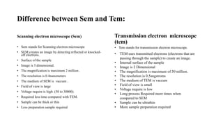
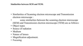
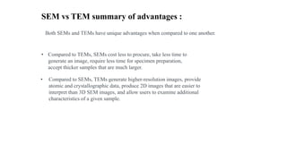
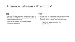
The document compares and contrasts scanning electron microscopes (SEM) and transmission electron microscopes (TEM). SEMs detect reflected electrons to image surface details in 3D, have lower resolution but larger fields of view than TEMs, and require less sample preparation. In contrast, TEMs transmit electrons through thin samples to image internal structures in 2D with higher resolution but smaller fields of view, and require more complex sample preparation. Both use vacuum environments and have adjustable magnification, but TEMs provide atomic-scale resolution and additional material characterization compared to SEMs.