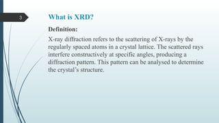
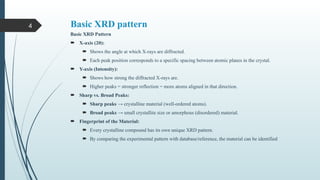
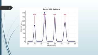
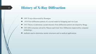
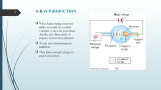
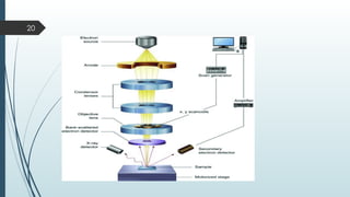
1
XRD(x-ray diffraction)
SEM(Scanning electron microscopy)
BY; BIBI HAFSA NAUDHANI
MS-CHEM
Analytical chemistry
2 WHAT IS X-RAY?
 Beams of electromagnetic radiation
 smaller wavelength than visible light,
 higher energy
 more penetrative
3 What is XRD?
Definition:
X-ray diffraction refers to the scattering of X-rays by the
regularly spaced atoms in a crystal lattice. The scattered rays
interfere constructively at specific angles, producing a
diffraction pattern. This pattern can be analysed to determine
the crystal’s structure.
4 Basic XRD pattern
Basic XRD Pattern
 X-axis (2θ):
 Shows the angle at which X-rays are diffracted.
 Each peak position corresponds to a specific spacing between atomic planes in the crystal.
 Y-axis (Intensity):
 Shows how strong the diffracted X-rays are.
 Higher peaks = stronger reflection = more atoms aligned in that direction.
 Sharp vs. Broad Peaks:
 Sharp peaks → crystalline material (well-ordered atoms).
 Broad peaks → small crystallite size or amorphous (disordered) material.
 Fingerprint of the Material:
 Every crystalline compound has its own unique XRD pattern.
 By comparing the experimental pattern with database/reference, the material can be identified
5
6 History of X-Ray Diffraction
 1895 X-rays discovered by Roentgen
 1914 First diffraction pattern of a crystal made by Knipping and von Laue
 1915 Theory to determine crystal structure from diffraction pattern developed by Bragg.
 1953 DNA structure solved by Watson and Crick Now Diffraction improved by computer
technology;
 methods used to determine atomic structures and in medical applications
7 X-RAY PRODUCTION
 When high energy electrons
strike an anode in a sealed
vacuum, x-rays are generated.
Anodes are often made of
copper, iron or molybdenum.
 X-rays are electromagnetic
radiation.
 They have enough energy to
cause ionization.
8
What is X-ray
Diffraction (XRD)
Most useful in the
characterisation of crystalline
materials; Ceramics, metals,
intermetallics, minerals,
inorganic compounds
rapid and nondestructive
techniques
Provide information on unit cell
dimension
9
COMPONENTS
X-ray source
Device for restricting
wavelength range
“goniometer”
Sample holder
Radiation detector
Signal processor and
readout
10
WORKING
• A continuous beam of
X-rays is incident on the crystal
• The diffracted
radiation is very intense in
certain directions
– These directions correspond
to constructive interference
from waves reflected from the
layers of the crystal
• The diffraction pattern
is detected by photographic film
11
PRINCIPLES OF XRD
Bragg’s Law
• The beam reflected from the
lower surface travels farther
than the one reflected from the
upper surface
• If the path difference equals
some integral multiple of the
wavelength, constructive
interference occurs
• Bragg’s Law gives the
conditions for constructive
Interference
nλ=2dsin⁡
θ
12 SCHEMATIC
13
14
Single Crystal X-ray Diffraction
Used to determine
 crystal structure
 orientation
 degree of crystalline perfection/imperfections (twinning, mozaicity, etc.)
 Sample is illuminated with monochromatic radiation
 Easier to index and solve the crystal structure because it diffraction peak is uniquely
resolved
15 X-ray Powder Diffraction
 More appropriately called polycrystalline X-ray diffraction, because it can also be used for
sintered samples, metal foils, coatings and films, finished parts, etc.
 Used to determine
 phase composition (commonly called phase ID)- what phases are present?
 quantitative phase analysis- how much of each phase is present?
 unit cell lattice parameters, crystal structure
 average crystallite size of nanocrystaline samples
 crystallite microstrain and texture
 residual stress (really residual strain)
16 Applications of X-Ray Diffraction
 Determination of Crystal structure
 Phase identification / transition
 Grain size / micro-strain
 Texture/stress( i.e.polymer , fiber )
 Determination of thin film composition
 Industry Identification of archeological materials
17
SEM(scanning electron
microscopy)
18 INTRODUCTION:
Scanning electron microscopes (SEMs) have become powerful and versatile tools for material
characterization, especially in recent years, as the size of materials used in various applications
continues to shrink. Electron microscopes use electrons for imaging in a similar way that light
microscopes use visible light. Unlike transmission electron microscopes (TEMs), which detect
electrons that pass through a very thin specimen, SEMs use the electrons that are reflected or
knocked off the near-surface region of a sample to create an image. Since the wavelength of
electrons is much smaller than that of light, the resolution of SEMs is superior to that of a light
microscope.
19
What is a Scanning Electron Microscope (SEM)?
The Scanning Electron Microscope (SEM), invented around 1965, utilizes signals such as
secondary electrons, backscattered electrons, and characteristic X-rays to observe and analyze
the morphology and features of sample surfaces. It is a method for observing microstructures
that lies between transmission electron microscopy and optical microscopy.
SEM can be equipped with accessories such as Energy Dispersive X-ray Spectroscopy (EDS),
Wavelength Dispersive X-ray Spectroscopy (WDS), and Electron Backscatter Diffraction
(EBSD), enabling simultaneous analysis of microstructure, texture, orientation differences, and
micro-area composition. It can also be equipped with devices such as heating and tensile
testing apparatus inside the sample chamber, allowing for in-situ and dynamic analysis of
samples.
Today, SEM finds wide applications in fields such as materials science, physics, chemistry,
biology, archaeology, geology, and the microelectronics industry.
20
21 Basic principle
A scanning electron microscope (SEM) operates by emitting an electron beam from an electron gun. When
high-energy electrons from this beam strike the surface of the sample, they excite regions which then emit
secondary electrons, backscattered electrons, absorbed electrons, Auger electrons, cathodoluminescence,
and characteristic X-rays. By receiving, amplifying, and displaying these signals as images, the features of
the sample surface can be observed, allowing for analysis of its morphology, structure, composition, and
other characteristics. SEM primarily utilizes signals such as secondary electrons, backscattered electrons,
and characteristic X-rays to analyse the features of the sample surface.
22 Secondary electrons refer to the outer-shell electrons of sample atoms that are excited by incident
electrons. Secondary electrons have low energy and can only escape the surface to a depth of a few
nanometres. Therefore, they are highly sensitive to the surface state of the sample and are primarily used
for observing the morphology of the sample surface in scanning electron microscopy.
Backscattered electrons are high-energy electrons that emerge from the sample surface after being
scattered (both elastically and in elastically) by incident electrons within the sample. Their energy is
similar to that of the incident electrons. The yield of backscattered electrons increases with the atomic
number of the sample elements. Therefore, the intensity of backscattered electron signals is related to the
chemical composition of the sample and can display atomic number contrast, making it useful for
qualitative analysis of sample composition.
23
Scanning Electron Microscope (SEM) Equipment
24
Applications of Scanning Electron Microscope (SEM):
 Observation of Nanomaterials: SEM has high resolution and can observe particles or microcrystal sizes
(0.1-100 nm) of composite materials.
 Analysis of Material Fracture Surfaces: SEM has great depth of field, rich three-dimensional images, and
can present the essence and fracture mechanism of material fracture morphology. It is suitable for
analyzing material fracture causes, accident reasons, and process rationality.
 Observation of Large Samples: It can directly observe samples with diameters of 100 mm, heights of 50
mm, or even larger sizes, without any restrictions on the shape of the sample. It can also observe rough
surfaces, which eliminates the trouble of preparing samples and allows for the observation of the
different contrasts of the sample's own material composition (backscattered electron image).
 Observation of Thick Samples: It provides high resolution and the most realistic morphology when
observing thick samples.
 Detailed Observation of Various Areas of the Sample: The sample has a large movable range in the
specimen chamber and can move in six degrees of freedom in three-dimensional space (i.e., three-
dimensional translation, three-dimensional rotation), making it convenient to observe various areas of
irregular samples.
 Observation of Samples at Low Magnifications with Large Field of View: Large field of view and low
magnification observation of samples are necessary in some fields such as forensic investigation and
archaeology.
25
“
”
SEM lets us see the surface,
XRD reveals the structure, they
uncover the beauty within the
smallest details of matter.
THANK YOU

X-ray diffraction and scanning electron microscopy.

  • 1.
    1 XRD(x-ray diffraction) SEM(Scanning electronmicroscopy) BY; BIBI HAFSA NAUDHANI MS-CHEM Analytical chemistry
  • 2.
    2 WHAT ISX-RAY?  Beams of electromagnetic radiation  smaller wavelength than visible light,  higher energy  more penetrative
  • 3.
    3 What isXRD? Definition: X-ray diffraction refers to the scattering of X-rays by the regularly spaced atoms in a crystal lattice. The scattered rays interfere constructively at specific angles, producing a diffraction pattern. This pattern can be analysed to determine the crystal’s structure.
  • 4.
    4 Basic XRDpattern Basic XRD Pattern  X-axis (2θ):  Shows the angle at which X-rays are diffracted.  Each peak position corresponds to a specific spacing between atomic planes in the crystal.  Y-axis (Intensity):  Shows how strong the diffracted X-rays are.  Higher peaks = stronger reflection = more atoms aligned in that direction.  Sharp vs. Broad Peaks:  Sharp peaks → crystalline material (well-ordered atoms).  Broad peaks → small crystallite size or amorphous (disordered) material.  Fingerprint of the Material:  Every crystalline compound has its own unique XRD pattern.  By comparing the experimental pattern with database/reference, the material can be identified
  • 5.
  • 6.
    6 History ofX-Ray Diffraction  1895 X-rays discovered by Roentgen  1914 First diffraction pattern of a crystal made by Knipping and von Laue  1915 Theory to determine crystal structure from diffraction pattern developed by Bragg.  1953 DNA structure solved by Watson and Crick Now Diffraction improved by computer technology;  methods used to determine atomic structures and in medical applications
  • 7.
    7 X-RAY PRODUCTION When high energy electrons strike an anode in a sealed vacuum, x-rays are generated. Anodes are often made of copper, iron or molybdenum.  X-rays are electromagnetic radiation.  They have enough energy to cause ionization.
  • 8.
    8 What is X-ray Diffraction(XRD) Most useful in the characterisation of crystalline materials; Ceramics, metals, intermetallics, minerals, inorganic compounds rapid and nondestructive techniques Provide information on unit cell dimension
  • 9.
    9 COMPONENTS X-ray source Device forrestricting wavelength range “goniometer” Sample holder Radiation detector Signal processor and readout
  • 10.
    10 WORKING • A continuousbeam of X-rays is incident on the crystal • The diffracted radiation is very intense in certain directions – These directions correspond to constructive interference from waves reflected from the layers of the crystal • The diffraction pattern is detected by photographic film
  • 11.
    11 PRINCIPLES OF XRD Bragg’sLaw • The beam reflected from the lower surface travels farther than the one reflected from the upper surface • If the path difference equals some integral multiple of the wavelength, constructive interference occurs • Bragg’s Law gives the conditions for constructive Interference nλ=2dsin⁡ θ
  • 12.
  • 13.
  • 14.
    14 Single Crystal X-rayDiffraction Used to determine  crystal structure  orientation  degree of crystalline perfection/imperfections (twinning, mozaicity, etc.)  Sample is illuminated with monochromatic radiation  Easier to index and solve the crystal structure because it diffraction peak is uniquely resolved
  • 15.
    15 X-ray PowderDiffraction  More appropriately called polycrystalline X-ray diffraction, because it can also be used for sintered samples, metal foils, coatings and films, finished parts, etc.  Used to determine  phase composition (commonly called phase ID)- what phases are present?  quantitative phase analysis- how much of each phase is present?  unit cell lattice parameters, crystal structure  average crystallite size of nanocrystaline samples  crystallite microstrain and texture  residual stress (really residual strain)
  • 16.
    16 Applications ofX-Ray Diffraction  Determination of Crystal structure  Phase identification / transition  Grain size / micro-strain  Texture/stress( i.e.polymer , fiber )  Determination of thin film composition  Industry Identification of archeological materials
  • 17.
  • 18.
    18 INTRODUCTION: Scanning electronmicroscopes (SEMs) have become powerful and versatile tools for material characterization, especially in recent years, as the size of materials used in various applications continues to shrink. Electron microscopes use electrons for imaging in a similar way that light microscopes use visible light. Unlike transmission electron microscopes (TEMs), which detect electrons that pass through a very thin specimen, SEMs use the electrons that are reflected or knocked off the near-surface region of a sample to create an image. Since the wavelength of electrons is much smaller than that of light, the resolution of SEMs is superior to that of a light microscope.
  • 19.
    19 What is aScanning Electron Microscope (SEM)? The Scanning Electron Microscope (SEM), invented around 1965, utilizes signals such as secondary electrons, backscattered electrons, and characteristic X-rays to observe and analyze the morphology and features of sample surfaces. It is a method for observing microstructures that lies between transmission electron microscopy and optical microscopy. SEM can be equipped with accessories such as Energy Dispersive X-ray Spectroscopy (EDS), Wavelength Dispersive X-ray Spectroscopy (WDS), and Electron Backscatter Diffraction (EBSD), enabling simultaneous analysis of microstructure, texture, orientation differences, and micro-area composition. It can also be equipped with devices such as heating and tensile testing apparatus inside the sample chamber, allowing for in-situ and dynamic analysis of samples. Today, SEM finds wide applications in fields such as materials science, physics, chemistry, biology, archaeology, geology, and the microelectronics industry.
  • 20.
  • 21.
    21 Basic principle Ascanning electron microscope (SEM) operates by emitting an electron beam from an electron gun. When high-energy electrons from this beam strike the surface of the sample, they excite regions which then emit secondary electrons, backscattered electrons, absorbed electrons, Auger electrons, cathodoluminescence, and characteristic X-rays. By receiving, amplifying, and displaying these signals as images, the features of the sample surface can be observed, allowing for analysis of its morphology, structure, composition, and other characteristics. SEM primarily utilizes signals such as secondary electrons, backscattered electrons, and characteristic X-rays to analyse the features of the sample surface.
  • 22.
    22 Secondary electronsrefer to the outer-shell electrons of sample atoms that are excited by incident electrons. Secondary electrons have low energy and can only escape the surface to a depth of a few nanometres. Therefore, they are highly sensitive to the surface state of the sample and are primarily used for observing the morphology of the sample surface in scanning electron microscopy. Backscattered electrons are high-energy electrons that emerge from the sample surface after being scattered (both elastically and in elastically) by incident electrons within the sample. Their energy is similar to that of the incident electrons. The yield of backscattered electrons increases with the atomic number of the sample elements. Therefore, the intensity of backscattered electron signals is related to the chemical composition of the sample and can display atomic number contrast, making it useful for qualitative analysis of sample composition.
  • 23.
  • 24.
    24 Applications of ScanningElectron Microscope (SEM):  Observation of Nanomaterials: SEM has high resolution and can observe particles or microcrystal sizes (0.1-100 nm) of composite materials.  Analysis of Material Fracture Surfaces: SEM has great depth of field, rich three-dimensional images, and can present the essence and fracture mechanism of material fracture morphology. It is suitable for analyzing material fracture causes, accident reasons, and process rationality.  Observation of Large Samples: It can directly observe samples with diameters of 100 mm, heights of 50 mm, or even larger sizes, without any restrictions on the shape of the sample. It can also observe rough surfaces, which eliminates the trouble of preparing samples and allows for the observation of the different contrasts of the sample's own material composition (backscattered electron image).  Observation of Thick Samples: It provides high resolution and the most realistic morphology when observing thick samples.  Detailed Observation of Various Areas of the Sample: The sample has a large movable range in the specimen chamber and can move in six degrees of freedom in three-dimensional space (i.e., three- dimensional translation, three-dimensional rotation), making it convenient to observe various areas of irregular samples.  Observation of Samples at Low Magnifications with Large Field of View: Large field of view and low magnification observation of samples are necessary in some fields such as forensic investigation and archaeology.
  • 25.
    25 “ ” SEM lets ussee the surface, XRD reveals the structure, they uncover the beauty within the smallest details of matter. THANK YOU