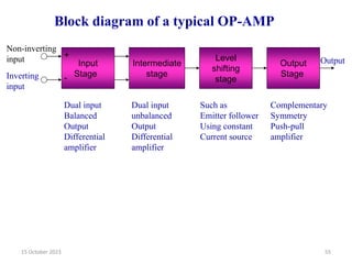
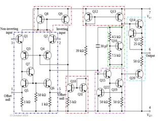
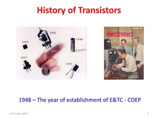
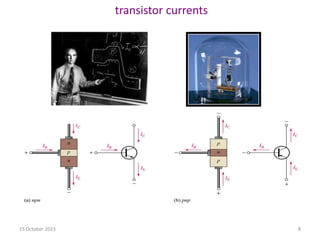
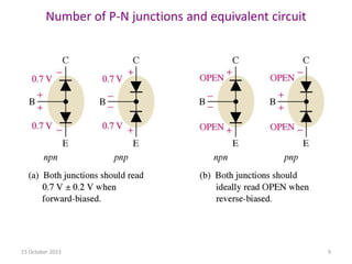
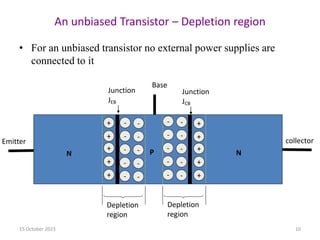
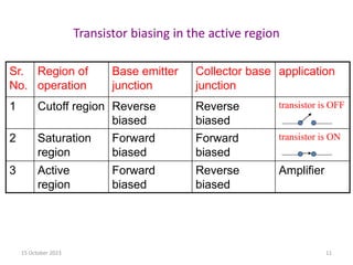
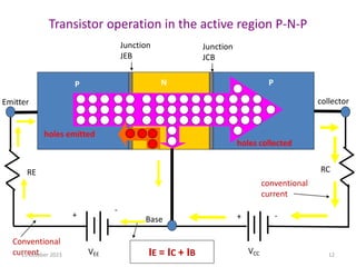
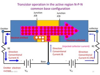
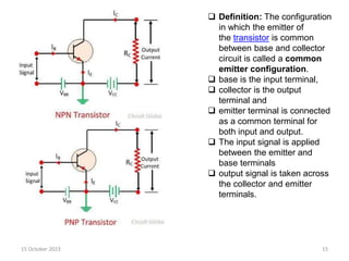
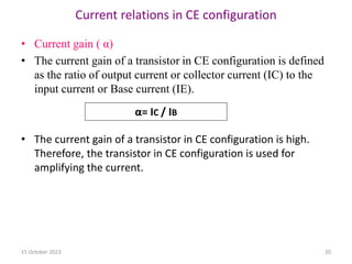
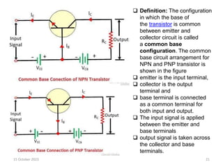
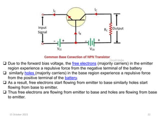
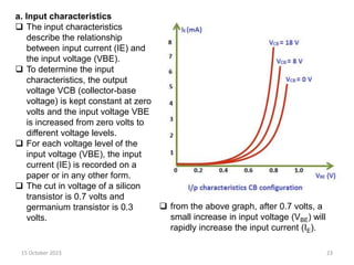
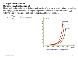
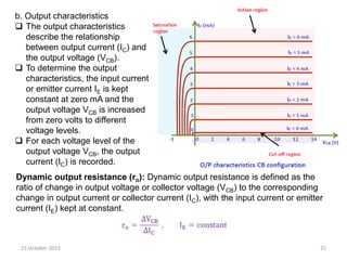
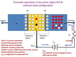
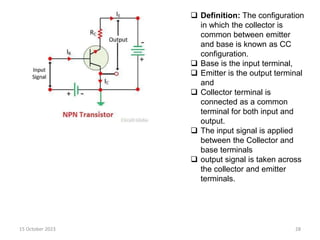
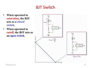
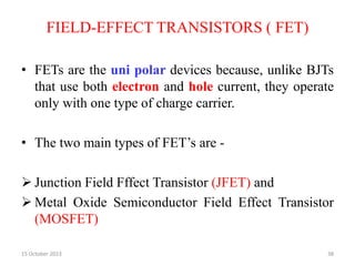
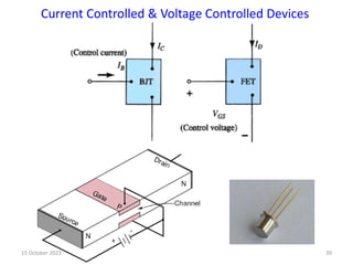
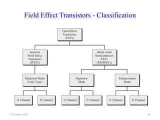
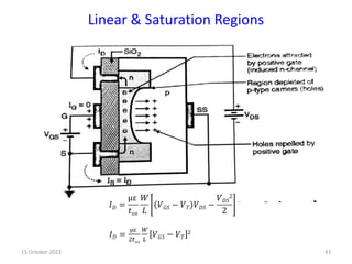
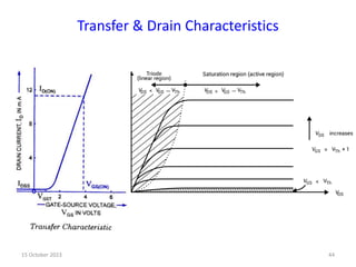
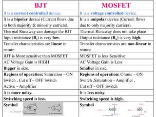
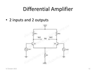
This document discusses transistors and operational amplifiers. It begins by providing an overview of the bipolar junction transistor (BJT), including its structure as a three-terminal device and how it can amplify small input signals at the collector. The document then covers transistor characteristics such as input and output characteristics, configurations including common emitter, common base, and common collector, and current relations. It also discusses MOSFETs and operational amplifiers at a high level.


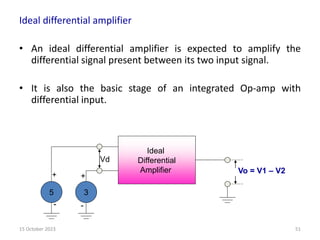
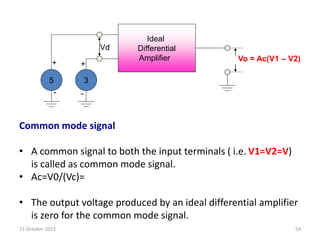
![Ideal
Differential
Amplifier (Ad=10)
3
5
Vd
Vo =Ad(V1 – V2)
+
+
-
-
Differential gain -
• Vo = Ad ( V1 – V2 )
Where Ad is called as the differential gain.
• The differential gain can be defined as the gain with which the
differential amplifier amplifies the differential signal.
Vo = Ad Vd as Vd = V1 – V2
Gain Ad = Vo / Vd decibel Vo=10 Vd 2V
Ad (dB) =10 log10 [ Vo / Vd ]
15 October 2023 53](https://image.slidesharecdn.com/unit2-231015171212-54165d99/85/Unit-2-pptx-53-320.jpg)