Processoer 80486
•Download as DOCX, PDF•
3 likes•4,765 views

The Intel 80486 microprocessor was an upgrade from the 80386 with improved performance and new features. It had an on-chip cache, floating point unit, and clock doubling capabilities. There were several variants including the 80486DX with an FPU, 80486SX without an FPU, and clock doubled 80486DX2. It had a 5-stage pipeline allowing one instruction per clock cycle. The integrated floating point unit and cache improved performance significantly over previous Intel processors.

More Related Content
What's hot
What's hot (20)
Viewers also liked
Viewers also liked (7)
Similar to Processoer 80486
Similar to Processoer 80486 (20)
More from University of Science Malaysia
Recently uploaded
Recently uploaded (20)
Processoer 80486
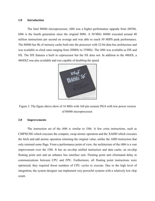
- 1. 1.0 Introduction The Intel 80486 microprocessor, i486 was a higher performance upgrade from i80386. I486 is the fourth generation since the original 8086. A 50 MHz 80486 executed around 40 million instructions per second on average and was able to reach 50 MIPS peak performance. The 80486 has 8k of memory cache built into the processor with 32-bit data bus architecture and was available in clock rates ranging from 20MHz to 33MHz. The i486 was available as DX and SX. The DX features a built in coprocessor but the SX does not. In addition to the 486SX, a 486SX2 was also available and was capable of doubling the speed. Figure 1: The figure above show of 16 MHz with 168 pin ceramic PGA with low power version of 80486 microprocessor. 2.0 Improvements The instruction set of the i486 is similar to i386. A few extra instructions, such as CMPXCHG which executes the compare, swap atomic operation and the XADD which executes the fetch and add atomic operation returning the original value, unlike the ADD instruction that only returned some flags. From a performance point of view, the architecture of the i486 is a vast improvement over the i386. It has an on-chip unified instruction and data cache, an on-chip floating point unit and an enhance bus interface unit. Floating point unit eliminated delay in communications between CPU and FPU. Furthermore, all floating point instructions were optimized, they required fewer numbers of CPU cycles to execute. Due to the high level of integration, the system designer can implement very powerful systems with a relatively low chip count.
- 2. The 486 has a 32-bit data bus and a 32-bit address bus. This required either four matched 30-pin (8-bit) SIMMs or one 72-pin (32-bit) SIMM on a typical PC motherboard. Just like the 80386, the 32-bit address bus of the 80486 enabled up to 4gigabytes of memory to be directly addressed using a flat memory model with 32-bit linear addresses in protected mode. Just as with the 80386, the ability to use memory directly without segmentation helped performance in compliant operating systems and applications. Moreover, clock-doubling and clock-tripling technology was also introduced in faster versions of Intel 80486 CPU. These i486 processors could run in existing motherboards with 20-33 MHz bus frequency, while running internally at two or three times of bus frequency. 80486SX2 and 80486DX2 were clock-doubled version, and 80486DX4 was a clock-tripled version. Power management features and System Management Mode (SMM) became a standard feature of the processor. One of the most obvious features of i486, is a built in math coprocessor. The coprocessor being integrated on the chip allows it to execute math operation 3 times faster than i386. To make room for data signal, it packaged in 168 pin, pin grid array packages instead 132 pin PGA used for i386. In addition, some aspects of the microprocessor's design have been streamlined to allow simplification of system design. Simple instructions execute in one clock cycle assuming the data is already in the cache. At the same clock rate, it yields a rough doubling in ALU performance. For example, a 16-MHz i486 therefore has a performance similar to a 33-MHz i386. 3.0 Type of 80486 Microprocessor The first important difference that the i486 has in comparison with its predecessor is that it has an integrated floating point unit on the chip itself. Previous processors had the arithmetic unit as a separate unit. The 8086 had 8087, the 80186 had the 80187, the 80286 had the 80287, and the 80386 had the 80387. Logically, the 80486 should have had an arithmetic co-processor 80487 external to the chip, but instead, Intel placed the arithmetic co-processor inside the chip and called the whole chip as 80486DX. To improve its market segment, Intel also sold a i486 processor without an FPU as the arithmetic co-processor. It was named as 80486SX, but in fact it was just the 80486 processor with its FPU turned off. 1. 80486DX
- 3. Clock rates a. 25 MHz with 20 MIPS (16.8 SPECint92, 7.40 SPECfp92) b. 33 MHz with 27 MIPS (22.4 SPECint92 on Micronics M4P 128 KB L2) c. 50 MHz with 41 MIPS (33.4 SPECint92, 14.5 SPECfp92 on Compaq/50L 256 KB L2) Bus Width 32 bits Number of Transistors a. 1.2 million at 1 µm b. the 50 MHz was at 0.8 µm Addressable memory 4 GB Virtual memory 1 TB Level 1 cache of 8 KB on chip Math coprocessor on chip 50X performance of the 8088 Used in Desktop computing and servers Family 4 model 3 2. 80486SX Clock rates: a. 16 MHz with 13 MIPS b. 20 MHz with 16.5 MIPS c. 25 MHz with 20 MIPS (12 SPECint92) d. 33 MHz with 27 MIPS (15.86 SPECint92 Bus Width 32 bits Number of Transistors a. 1.185 million at 1 µm b. 2900,000 at 0.8 µm Addressable memory 4 GB Virtual memory 1 TB Identical in design to 486DX but without math coprocessor. The first version was an 80486DX with disabled math coprocessor in the chip and different pin configuration.
- 4. If the user needed math coprocessor capabilities, he must add 487SX which was actually an 486DX with different pin configuration to prevent the user from installing a 486DX instead of 487SX, so with this configuration 486SX+487SX you had 2 identical CPU's with only 1 effectively turned on Used in low-cost entry to 486 CPU desktop computing, as well as extensively used in low cost mobile computing. Upgradable with the Intel OverDrive processor Family 4 model 2 3. 80486DX2 The internal cache improved the memory access speed substantially, but later versions had something called clock doubling. New editions were released with higher clock frequencies, as they hit on the idea of doubling the internal clock frequency in relation to the external clock. These double-clocked processors were given the name, 80486DX2. A very popular model in this series had an external clock frequency of 33 MHz while working at 66 MHz internally. The characteristics of 80486DX2 are: Runs at twice the speed of the external bus (FSB). Fits on Socket 3 Clock rates: a. 40 MHz b. 50 MHz c. 66 MHz d. 100MHz (this was only made for a short time due to high failure rates) 4. 80486SL Clock rates: a. 20 MHz with 15.4MIPS b. 25 MHz with 19 MIPS c. 33 MHz with 25 MIPS Bus Width 32 bits Number of Transistors 1.4 million at 0.8 µm Addressable memory 4 GB Virtual memory 1 TB
- 5. Used in notebook computers Family 4 model 3 5. 80486DX4 Clock rates: a. 75 MHz with 53 MIPS (41.3 SPECint92, 20.1 SPECfp92 on Micronics M4P 256 KB L2) b. 100 MHz with 70.7 MIPS (54.59 SPECint92, 26.91 SPECfp92 on Micronics M4P 256 KB L2) Number of Transistors 1.6 million at 0.6 µm Bus width 32 bits Addressable memory 4 GB Virtual memory 64 TB Pin count 168 PGA Package, 208 sq ftP Package Used in high performance entry-level desktops and value notebooks Family 4 model 8
- 6. Figure 2: The figure above show of 486DX2 architecture The Instruction Pipeline The instruction pipeline consists of three basic parts. At a given moment in time, a series of instructions are in the pipeline at various stages. The ability of the 80486 microprocessor to process a number of instructions in parallel gives it the ability to complete execution of an instruction during each cycle of the processor clock (PCLK). However, this capability depends on the particular instructions in the instruction stream.
- 7. Figure 3: The figure show of five stage pipeline of the 80486. The i486 is a heavily pipelined processor. It has a 5 stage pipeline as shown in Figure 3. Each stage takes one clock cycle, but once the pipeline is full, each instruction will execute in a single clock. The stages in the pipeline are as Pre-fetch, decode1, decode2, execute and write back. I1 to I5 correspond to five instructions in the pipeline. As per this figure, there are two decoding stages. This is because of the varied addressing modes of 80486 and the necessity for protection checks before any access is allowed. Instruction prefetch In computer architecture, instruction prefetch is a technique used in microprocessors to speed up the execution of a program by reducing wait states. Modern microprocessors are much faster than the memory where the program is kept, meaning that the program's instructions cannot be read fast enough to keep the microprocessor busy. Adding a cache can provide faster access to needed instructions. Prefetching occurs when a processor requests an instruction from main memory before it is actually needed. Once the instruction comes back from memory, it is placed in a cache. When an instruction is actually needed, the instruction can be accessed much more quickly from the cache than if it had to make a request from memory. Since programs are generally executed sequentially, performance is likely to be best when instructions are prefetched in program order. Alternatively, the prefetch may be part of a complex branch prediction algorithm, where the processor tries to anticipate the result of a calculation and fetch the right instructions in advance. In the case of dedicated hardware (like a Graphics Processing Unit) the prefetch can
- 8. take advantage of the spatial coherence usually found in the texture mapping process. In this case, the prefetched data are not instructions, but texture elements (texels) that are candidates to be mapped on a polygon. The first mainstream microprocessors to use some form of instruction prefetch were the Intel 8086 (six bytes) and the Motorola 68000 (four bytes). Decode stage 1 (D1) • Opcode & address-mode info • At most first 3 bytes of instruction • Can direct D2 stage to get rest of instruction Decode stage 2 (D2) • Expand opcode into control signals • Computation of complex address modes Execute (EX) • ALU operations, cache access, register update Writeback (WB) • Update registers & flags • Results sent to cache & bus interface write buffers i486 i386 1. Tightly coupled pipelining allows a simple instruction completed in one clock cycle. 1. Need 2 clock cycles to complete simple instructions. 2. Have internal cache 2. No internal cache. 3. Level 1 cache increased to 16kB. 3. Level 1 cache 8kB. 4. First build with floating point unit. 4. Do not have floating point unit. Table 1: The table show of difference between i486 and i386. Internal Cache The internal cache introduced by Intel in the 486 processor provides the additional benefit of limiting the number of memory accesses that the processor must submit to external
- 9. memory. The 486's internal cache keeps a copy of the most recently used instructions and data. The processor only has to access slow external memory when it experiences an internal cache read miss or a memory write. The 486 employs a burst transfer mechanism to speed up transfers from external memory. Each internal cache miss forces the processor to access slow external memory. Because the internal cache's line size is 16 bytes, four complete bus cycles would be required to transfer the whole cache line (because the 486 only has a 32-bit data path). The burst transfer capability permits the processor to complete the four transfers faster than it could with zero wait state bus cycles. If the DRAM subsystem utilizes interleaved memory architecture, the transfers can complete faster than would be possible otherwise. The Advantage of a Level 2 Cache Some 486 systems use two levels of cache to improve overall system performance. The internal, or level one (L1), cache provides the processor with the most often used code and data, while the level two (L2) cache provides the processor with code and data that the L1 cache was too small to retain. Since all information destined for the internal L1 cache must pass through the external L2 cache, the advantage of the L2 cache may not be immediately apparent. If the L2 cache were the same size as the L1 cache (8KB), there would be no advantage. If, however, the L2 cache is substantially larger than the L1 cache, the advantage becomes clear. L2 caches are usually much larger (64KB- 512KB) than the 486 L1 cache. L2 caches improve overall performance because the L1 cache can get information from the L2 cache quickly on most internal read misses. Furthermore, most L2 caches can take full advantage of the 486 burst cycles to accommodate the fastest possible burst transfer. Consider the case if the L2 cache were sixteen times larger than the internal cache, or 128KB, in size. At a given moment in time, the L2 cache would contain a mirror image of the internal cache's contents and up to fifteen images of the internal cache's previous contents. The net result would be that, as long as the microprocessor is accessing memory locations that are cached in the internal cache, no bus activity to main DRAM need take place. When the microprocessor attempts to access a memory location that isn't cached in the internal cache, an external memory access would be initiated. If the microprocessor had previously accessed the same area of
- 10. memory, there is a high probability that it will be found in the L2 cache and can be burst back to the microprocessor. Only when a read miss occurs in both the internal and L2 caches would an access to the slow DRAM main memory become necessary. Power Management and SMM 2. Fast SMI with separate memory space 3. Fully static design permits dynamic clock control 4. Software or hardware initiates low power suspend mode 5. Automatic FPU power-down mode REFERENCES [1] Tom Shanley (1995). “The 80486 System Architecture”. Addison Wesley Publishing Company. [2] (2010). “Intel 80846 microprocessor family”. Central Processing Unit. Retrieved at 12 May 2013 from http://www.cpu-world.com/CPUs/80486/ [3] (2008). “Study of Intel 80486 Processor”. Advanced Microprocessor Features. Mission 10X. Retrieved at 12 May 2013 from http://www.mission10x.com/mission- 10x/Documents/Microprocessor_Unit3/U3-S11_Ver_Final.pdf [4] “The Enhance Features of 80486”. Safari Book Online. Retrieved at 12 May 2013 from http://my.safaribooksonline.com/book/hardware/9788131732465/the-pentium- processor/ch16lev1sec2