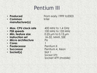
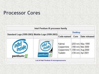
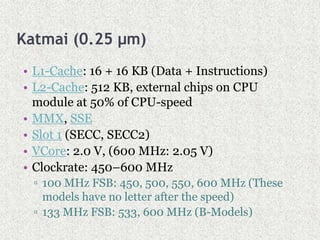
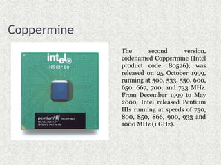
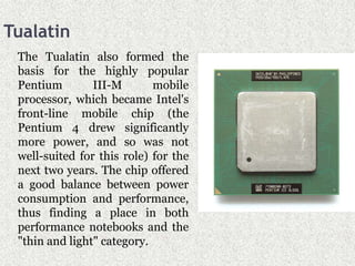
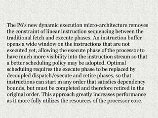
The Pentium III was a desktop and mobile CPU produced by Intel between 1999-2003. It had clock speeds between 400 MHz to 1.4 GHz and included features like MMX and SSE instructions. There were several stepping of the Pentium III including Katmai at 0.25 μm, Coppermine at 0.18 μm, Coppermine T at 0.18 μm, and Tualatin at 0.13 μm. Each stepping improved performance through higher clock speeds, larger caches, and support for newer instruction sets. Optimizing code for the Pentium III microarchitecture required techniques like scheduling instructions to maximize decoder throughput, balancing usage of execution units, and minimizing register dependencies. The Pentium III was also notable for including
found this one in one of my abandoned folders. AC(students from JUCSE need no introduction but for others you should never want to know him :-O) assigned this task to me and 3 of my fellow classmates to create a presentation on this uninteresting and weird topic. We pulled it off however :P
Origin of Microprocessor and Classification of Microprocessor Vijay Kumar
This Presentation have information about the topics are
Microprocessors evolution,
Introduction to 8085,
Basic terms,
Types of Processors,
Microprocessor Based System,
Origin of Microprocessor,
Classification of Microprocessor,
Memory,
Input and Output Devices and
Technological Improvements on Microprocessor.
PIC A special purpose integrated circuit that function as an overall manager in an interrupt driven system.
It accepts request from the peripheral equipment,determines which of the incoming request is of the highest priority, ascertains whether the incoming request has a higher priority value than the level currently being serviced, and issues an interrupt to the CPU based on this determination.
Where we are, as Front-End developers? This presentation navigates a short timeline of the computer science focusing on the client-side development as a mean to answer why and what has changed, as well as explore patterns and tendencies for the near future.
English article: https://medium.com/@caiovaccaro/javascript-state-of-the-union-2015-part-1-7ccff74813fa#.8x9y48ohk
ccfghlm,,fghggjjghkgkjkjkjklhljhlkjhljhlhjl
bnjkhhkbkbn,mn,mn,mn,mn,mn,mn,m,mn,bn,bn,mbn,bj,bjbj,bjbj,bm, dvglksmndgopjpjmlkvmsodfgjhonjhlkmnlkmdvokji0fpqokdf[k[akfmcadokjvojisdlkmlkswopdvgopko;pmfasd f
\plvsf[prblpk[bnpk
4. Katmai
• It was first released at speeds of 450 and
500 MHz in February 1999. Two more versions
were released: 550 MHz on May 17, 1999 and
600 MHz on August 2, 1999. On September 27,
1999 Intel released the 533B and 600B running
at 533 & 600 MHz respectively.
• The Katmai contains 9.5 million transistors, not
including the 512 Kbytes L2 cache (which adds
25 million transistors), and has dimensions of
12.3 mm by 10.4 mm (128 mm2).
5. Katmai (0.25 µm)
• L1-Cache: 16 + 16 KB (Data + Instructions)
• L2-Cache: 512 KB, external chips on CPU
module at 50% of CPU-speed
• MMX, SSE
• Slot 1 (SECC, SECC2)
• VCore: 2.0 V, (600 MHz: 2.05 V)
• Clockrate: 450–600 MHz
▫ 100 MHz FSB: 450, 500, 550, 600 MHz (These
models have no letter after the speed)
▫ 133 MHz FSB: 533, 600 MHz (B-Models)
6.
7. Coppermine
The second version,
codenamed Coppermine (Intel
product code: 80526), was
released on 25 October 1999,
running at 500, 533, 550, 600,
650, 667, 700, and 733 MHz.
From December 1999 to May
2000, Intel released Pentium
IIIs running at speeds of 750,
800, 850, 866, 900, 933 and
1000 MHz (1 GHz).
9. Coppermine T
• This revision is an intermediate step between Coppermine
and Tualatin, with support for lower-voltage system logic
present on the latter but core power within previously defined
voltage specs of the former so it could work in older system
boards.
• Intel used the latest Coppermines with the cD0-Stepping and
modified them so that they worked with low voltage system
bus operation at 1.25 V AGTL as well as normal 1.5 V AGTL+
signal levels, and would auto detect differential or single-
ended clocking. This modification made them compatible to
the latest generation Socket-370 boards supporting FC-PGA2
packaged CPUs while maintaining compatibility with the
older FC-PGA boards. The Coppermine T also had two way
symmetrical multiprocessing capabilities, but only in FC-
PGA2 boards.
• They can be distinguished from Tualatin processors by their
part numbers, which include the digits: 80533 e.g. the
1133 MHz SL5QK P/N is: RK80533PZ006256, while the
1000 MHz SL5QJ P/N is: RK80533PZ001256.
10. Coppermine T (0.18 µm)
• L1-Cache: 16 + 16 KB (Data + Instructions)
• L2-Cache: 256 KB, fullspeed
• MMX, SSE
• Socket 370 (FC-PGA, FC-PGA2)
• Front side bus: 133 MHz
• VCore: 1.75 V
• First release: June 2001
• Clockrate: 800–1133 MHz
▫ 133 MHz FSB: 800, 866, 933, 1000, 1133 MHz
11. Tualatin
The Tualatin also formed the
basis for the highly popular
Pentium III-M mobile
processor, which became Intel's
front-line mobile chip (the
Pentium 4 drew significantly
more power, and so was not
well-suited for this role) for the
next two years. The chip offered
a good balance between power
consumption and performance,
thus finding a place in both
performance notebooks and the
"thin and light" category.
13. Intel Pentium III microarchitecture
The Intel P6 core, introduced with the Pentium Pro processor and used in all
current Intel processors, features a RISC-like microarchitecture and an out-of-
order execution unit, representing a radical shift from previous designs.
14. The P6's new dynamic execution micro-architecture removes
the constraint of linear instruction sequencing between the
traditional fetch and execute phases. An instruction buffer
opens a wide window on the instructions that are not
executed yet, allowing the execute phase of the processor to
have much more visibility into the instruction stream so that
a better scheduling policy may be adopted. Optimal
scheduling requires the execute phase to be replaced by
decoupled dispatch/execute and retire phases, so that
instructions can start in any order that satisfies dependency
bounds, but must be completed and therefore retired in the
original order. This approach greatly increases performance
as it more fully utilizes the resources of the processor core.
15.
16. The P6 core executes x86 instructions by breaking them into simpler
micro-instructions called micro-ops. This task is performed by three
parallel decoders in the D1 stage of the pipeline: the first decoder is
capable of decoding one x86 instruction of four or fewer µops in each
clock cycle, while the other two decoders can each decode an x86
instruction of one µop in each clock cycle. Once the µops are decoded,
they will be issued from the in-order front-end into the Reservation
Station (RS), which is the beginning stage of the out-of-order core. In
the RS, the µops wait until their data operands are available; once a µop
has all data sources available, it will be dispatched from the RS to an
execution unit. Once the µop has been executed it returns to the
ReOrder Buffer and waits for retirement. In this stage, all data values
are written back to memory and all µops are retired in-order, three at a
time. The P6 core can schedule at a peak rate of 5 micro-ops per clock,
one to each resource port, but a sustained rate of 3 micro-ops per clock
is more typical.
17. Optimizing code for the P6 core is strikingly different than on previous
processors, such as the Pentium, that featured in-order execution. The
developer has no control over the sequence of execution, but the goal is
maximizing the efficiency of both the decoders and the execution units.
Pushing the decoding bandwidth to the limit means scheduling instructions
with a 4-1-1 pattern, where these numbers refer to the count of micro-ops
generated by each instruction. When working with MMX instructions, all
opcodes require only 1 micro-op except for computations that have as source
operand a memory reference, and writes to memory. The MMX register set
contains only 8 registers, therefore there are many instructions that use a
memory reference as source operand, and the fact that this kind of instruction
can only by translated by decoder 0 leads to stalls in this stage of the pipeline.
The only method for relieving this problem is choosing a smart register
allocation strategy that minimizes the number of memory references.
18.
19. The effective usage of the execution units is even more troublesome. There
are five execution units on the P6 core, and each performs a well-defined
set of operations: scheduling a large bulk of instructions of the same kind
will overcharge the required execution unit that will impose long latencies,
while all other execution units remain idle. The key to fast performance is
obtaining from the decoders a balanced stream of micro-ops that evenly
exploits all execution units, and this often means that loops must be
rearranged as most of them expose a great locality (i.e. loads from memory
at the beginning, computations in the middle and stores to memory at the
end).
Another key technique is minimizing dependency bounds among micro-
ops, so that they do not stall often waiting for data operands: the easiest
way to maximize the Instruction Level Parallelism (ILP) is unrolling loops
and scheduling two or more computing threads together. While this is
hardly a novel technique, actually implementing it is really complex due to
the limited number of MMX registers available, and a clever register
allocation strategy is mandatory.
20. It is therefore evident that writing high-performance MMX code requires much more
that the knowledge of the instruction set: the developer should have a solid background
on both traditional compiler designs to devise an effective register allocation strategy,
and on the microarchitectures of current processors to avoid pitfalls in the hand-
scheduled code.
Quexal implements an optimizing compiler that exploits all these techniques. The source
listing is re-arranged to maximize the Instruction Level Parallelism (ILP), then the
instructions are scheduled so that:
1. they satisfy the 4-1-1 pattern to fully use all decoders;
2. the resulting stream of micro-ops is balanced and makes effective usage of available
hardware resources;
3. the number of required registers does not exceed that of MMX registers.
The Quexal compiler outputs high-quality code that matches the speed of hand-
optimized samples. Performance benchmarks show that produced code usually makes
optimal usage of the decoders and achieves a typical 3 micro-ops per cycle rate, without
introducing excessive register spilling to memory.
21. Controversy about privacy issues
• The Pentium III was the first x86 CPU to include a unique,
retrievable, identification number, called PSN (Processor
Serial Number). A Pentium III's PSN can be read by software
through the CPUID instruction if this feature has not been
disabled through the BIOS.
• On November 29, 1999, the Science and Technology Options
Assessment (STOA) Panel of the European Parliament,
following their report on electronic surveillance techniques
asked parliamentary committee members to consider legal
measures that would "prevent these chips from being installed
in the computers of European citizens."[13]
• Eventually Intel decided to remove the PSN feature on
Tualatin-based Pentium IIIs, and the feature was not carried
through to the Pentium 4 or Pentium M. The feature does not
exist in modern Intel x86 CPUs.
The Pentium III brand refers to Intel's 32-bit x86 desktop and mobile microprocessors based on the sixth-generation P6 microarchitecture introduced on February 26, 1999. The brand's initial processors were very similar to the earlier Pentium II-branded microprocessors. The most notable difference was the addition of the SSEinstruction set (to accelerate floating point and parallel calculations), and the introduction of a controversial serial number embedded in the chip during the manufacturing process.
Similarly to the Pentium II it superseded, the Pentium III was also accompanied by the Celeron brand for lower-end versions, and the Xeon for high-end (server and workstation) derivatives. The Pentium III was eventually superseded by the Pentium 4, but its Tualatin core also served as the basis for the Pentium MCPUs, which used many ideas from the P6 microarchitecture. Subsequently, it was the Pentium M microarchitecture of Pentium M branded CPUs, and not the NetBurst found in Pentium 4 processors, that formed the basis for Intel's energy-efficient Core microarchitecture of CPUs branded Core 2, Pentium Dual-Core, Celeron (Core), and Xeon.
The first Pentium III variant was the Katmai (Intel product code 80525). It was a further development of the Deschutes Pentium II. The Pentium III saw an increase of 2 million transistors over the Pentium II. The differences were the addition of execution units and SSE instruction support, and an improved L1 cache controller (the L2 cache controller was left unchanged, as it would be completely redesigned for Coppermine anyway), which were responsible for the minor performance improvements over the "Deschutes" Pentium IIs.
Before the addition of the heat spreader, it was sometimes difficult to install a heatsink on a Pentium III. One had to be careful not to put force on the core at an angle because doing so would cause the edges and corners of the core to crack and could destroy the CPU. It was also sometimes difficult to achieve a flat mating of the CPU and heatsink surfaces, a factor of critical importance to good heat transfer. This became increasingly challenging with the socket 370 CPUs, compared with their Slot 1 predecessors, because of the force required to mount a socket-based cooler and the narrower, 2-sided mounting mechanism (Slot 1 featured 4-point mounting). As such, and because the 0.13 µm Tualatin had an even smaller core surface area than the 0.18 µm Coppermine, Intel installed the metal heatspreader on Tualatin and all future desktop processors.The Tualatin core was named after the Tualatin Valley and Tualatin River in Oregon, where Intel has large manufacturing and design facilities.