Downloaded 493 times

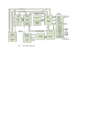

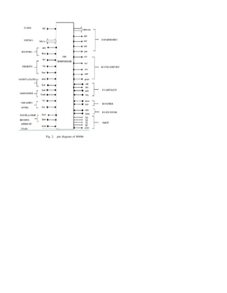
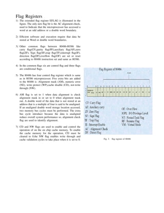
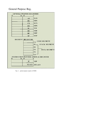


The document discusses the Intel 80486 microprocessor. Some key points: 1) The 80486 is an evolutionary step up from the 80386, integrating the math coprocessor on the chip for faster performance. 2) It has an 8KB internal code and data cache, a floating point unit, and 168 pins in a pin grid array package. 3) The architecture includes address and data buses, cache control signals, and status flags in registers like the 80386. It supports protected mode with virtual memory and multitasking capabilities.