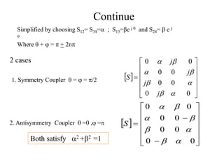
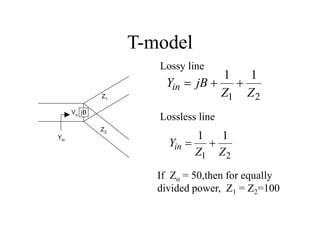
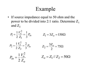
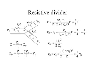
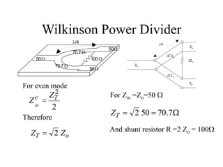
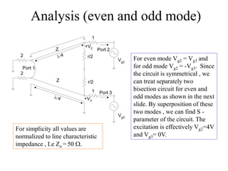
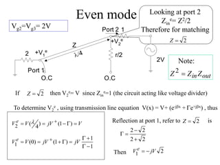
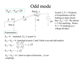
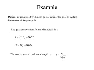
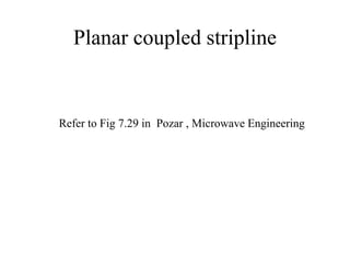
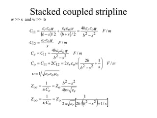
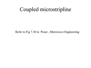
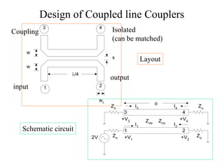
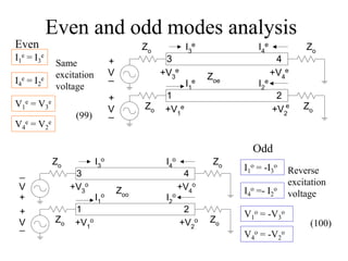
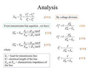
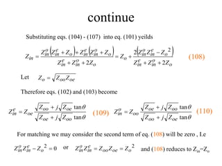
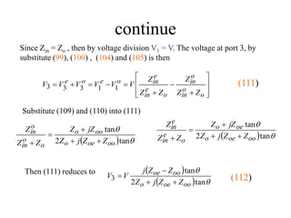
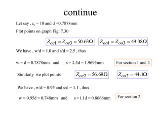
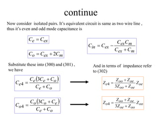
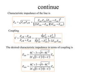
This document discusses power dividers, combiners, couplers, and their S-parameter representations. It covers basic properties of reciprocal and lossless networks, as well as examples like directional couplers. Key points include:
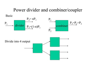
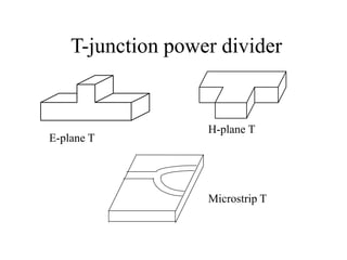
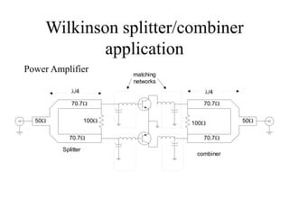
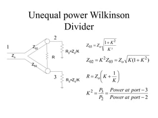
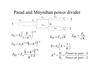
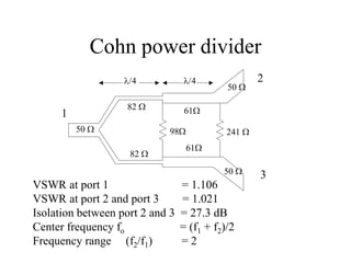
- Power dividers split power from one port to multiple ports, while combiners combine power from multiple ports into one port.
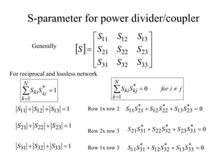
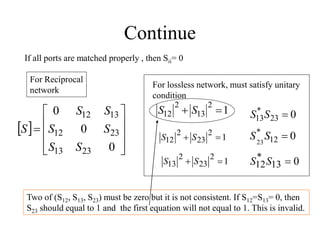
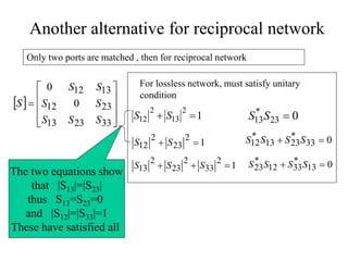
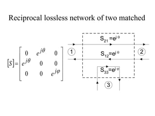
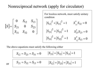
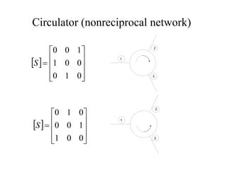
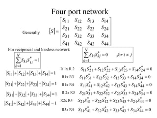
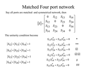
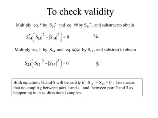
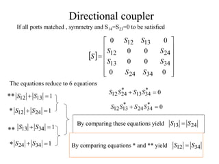
- S-parameters describe the scattering properties of networks and must satisfy unitary conditions for lossless, reciprocal networks.
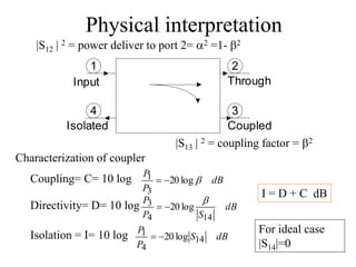
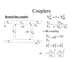
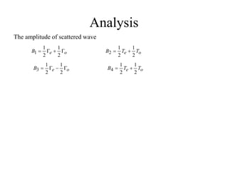
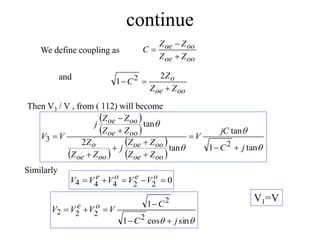
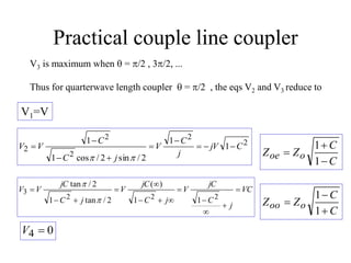
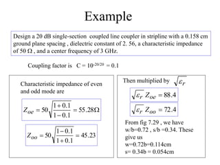
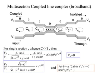
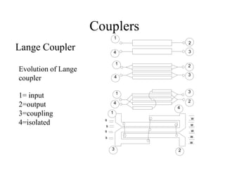
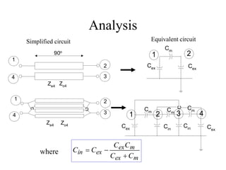
- A directional coupler has four ports where power is coupled from one port to another according to coupling factors while ensuring isolation between other ports.
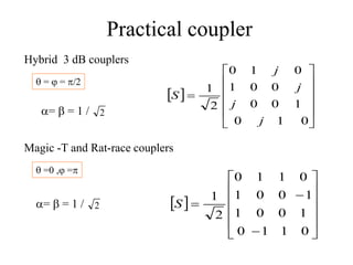
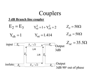
- An ideal 3 dB coupler has a 50% power split between the input and
![RF Circuit Design - [Ch3-2] Power Waves and Power-Gain Expressions](https://cdn.slidesharecdn.com/ss_thumbnails/ch3-2-150613064404-lva1-app6891-thumbnail.jpg?width=640&height=640&fit=bounds)
![RF Circuit Design - [Ch2-1] Resonator and Impedance Matching](https://cdn.slidesharecdn.com/ss_thumbnails/ch2-1-150613064353-lva1-app6892-thumbnail.jpg?width=640&height=640&fit=bounds)


![RF Circuit Design - [Ch2-2] Smith Chart](https://cdn.slidesharecdn.com/ss_thumbnails/ch2-2-150613064401-lva1-app6891-thumbnail.jpg?width=640&height=640&fit=bounds)

![RF Circuit Design - [Ch4-2] LNA, PA, and Broadband Amplifier](https://cdn.slidesharecdn.com/ss_thumbnails/ch4-2-150613064410-lva1-app6891-thumbnail.jpg?width=640&height=640&fit=bounds)


![射頻電子 - [第四章] 散射參數網路](https://cdn.slidesharecdn.com/ss_thumbnails/ch4-150613065103-lva1-app6891-thumbnail.jpg?width=640&height=640&fit=bounds)


![RF Circuit Design - [Ch3-1] Microwave Network](https://cdn.slidesharecdn.com/ss_thumbnails/ch3-1-150613064402-lva1-app6892-thumbnail.jpg?width=640&height=640&fit=bounds)


![5G Explained! A High Level Overview [Introduction]](https://cdn.slidesharecdn.com/ss_thumbnails/5gexplainedahighleveloverview-260119165306-cc137a3e-thumbnail.jpg?width=640&height=640&fit=bounds)


