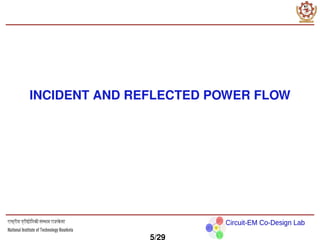
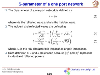
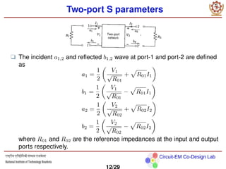
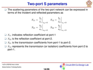
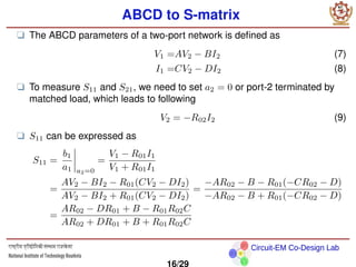
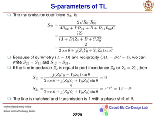
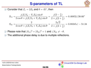
National Institute of Technology
Rourkela
Scattering Parameters
EE3004 : Electromagnetic Field Theory
Dr. Rakesh Sinha
(Assistant Professor)
Circuit and Electromagnetic Co-Design Lab at NITR
Department of Electrical Engineering
National Institute of Technology (NIT) Rourkela
March 31, 2023
Circuit-EM Co-Design Lab
Outline
1 Introduction
2 INCIDENT AND REFLECTED POWER FLOW
3 Two-port S parameters
4 ABCD to S-matrix
5 S-parameters of TL
6 S-parameters of Series and Shunt Elements
2/29
Circuit-EM Co-Design Lab
Introduction
3/29
Circuit-EM Co-Design Lab
Introduction
❑ Scattering parameters or S-parameters (the elements of a scattering
matrix or S-matrix) describe the electrical behavior of linear electrical
networks when undergoing various steady state stimuli by electrical
signals.
❑ The S-parameters are members of a family of similar parameters, other
examples being: Y-parameters, Z-parameters, H-parameters,
T-parameters or ABCD-parameters.
❑ They differ from these, in the sense that S-parameters do not use open or
short circuit conditions to characterize a linear electrical network; instead,
reference load or source impedances are used.
❑ Because of finite load conditions the S-parameters always exist, while
other parameters may not exist for certain network.
❑ The magnitude square of S-parameters represents power ratio of
reflected wave or transmitted wave to incident wave.
❑ The phase of S-parameters represents voltage phase difference between
reflected wave or transmitted wave and incident wave.
4/29
Circuit-EM Co-Design Lab
INCIDENT AND REFLECTED POWER FLOW
5/29
Circuit-EM Co-Design Lab
Transmission Line Equation
❑ The telegrapher’s equations of transmission line can be written as
V (z) = Vie−γz
+ Vreγz
(1a)
I(z) = Iie−γz
+ Ireγz
=
Vi
Z0
e−γz
−
Vr
Z0
eγz
(1b)
❑ Solving above equations simultaneously, we obtain explicit expressions
for the incident and reflected waves
Vie−γz
=
1
2
[V (z) + Z0I(z)] (2a)
Vreγz
=
1
2
[V (z) − Z0I(z)] (2b)
❑ The voltage wave based S-parameters can be written as
Vreγz
= ΓVie−γz
(2c)
6/29
Circuit-EM Co-Design Lab
S-parameter of a one port network
❑ The S-parameter of a one port network is defined as
b = Sa (3)
where b is the reflected wave and a is the incident wave.
❑ The incident and reflected waves are defined as
a =
Vie−γz
√
Z0
=
1
2

V
√
Z0
+
p
Z0I

(4)
b =
Vreγz
√
Z0
=
1
2

V
√
Z0
−
p
Z0I

(5)
where Z0 is the real characteristic impedance or port impedance.
❑ Such definition of a and b are chosen because |a|2
and |b|2
represent
incident and reflected powers.
7/29
Circuit-EM Co-Design Lab
One port network
❑ To understand the physical meaning of a and b, consider the power
dissipated by the one-port network
P =
1
2
Re V I∗
(6)
where I∗
denotes the complex conjugate of I.
❑ We can write V and I in terms of the incident and reflected parameters as
V =
p
Z0(a + b) I =
a − b
√
Z0
8/29
Circuit-EM Co-Design Lab
One port Network
❑ Then the power dissipated by the one-port network is
P =
1
2
(aa∗
− bb∗
)
=
1
2
|a|2
− |b|2

❑ The term 1
2 aa∗
can be interpreted as the power incident, while 1
2 bb∗
can
be regarded as the power reflected.
❑ The difference yields the power dissipated by the one-port network.
❑ The incident parameter a and the reflected parameter b are related by the
equation
b = Sa
where S is called the scattering element or, more commonly, the
reflection coefficient.
❑ From the definitions of a and b we can make the following substitution:

V
√
R0
−
p
R0I

= S

V
√
R0
+
p
R0I

9/29
Circuit-EM Co-Design Lab
One port Network
❑ Solving for S, we obtain
S =
Z − R0
Z + R0
where Z is the impedance of the one-port network
Z =
V
I
❑ A further useful result is that when the impedance R0 is set equal to the
impedance Z, the reflected parameter b = 0.
10/29
Circuit-EM Co-Design Lab
Two-port S parameters
11/29
Circuit-EM Co-Design Lab
Two-port S parameters
❑ The incident a1,2 and reflected b1,2 wave at port-1 and port-2 are defined
as
a1 =
1
2

V1
√
R01
+
p
R01I1

b1 =
1
2

V1
√
R01
−
p
R01I1

a2 =
1
2

V2
√
R02
+
p
R02I2

b2 =
1
2

V2
√
R02
−
p
R02I2

where R01 and R02 are the reference impedances at the input and output
ports respectively.
12/29
Circuit-EM Co-Design Lab
Two-port S parameters
❑ The scattering parameters Sij for the two-port network are given by the
equations
b1 = S11a1 + S12a2
b2 = S21a1 + S22a2
❑ In matrix form the set of above equations becomes

b1
b2

=

S11 S12
S21 S22
 
a1
a2

where the matrix
[S] =

S11 S12
S21 S22

is called the scattering matrix of the two-port network.
13/29
Circuit-EM Co-Design Lab
Two-port S parameters
❑ The scattering parameters of the two-port network can be expressed in
terms of the incident and reflected parameters as
S11 =
b1
a1 a2=0
S12 =
b1
a2 a1=0
S21 =
b2
a1 a2=0
S22 =
b2
a2 a1=0
❑ S11 indicates reflection coefficient at port-1
❑ S22 is the reflection coefficient at port-2.
❑ S21 is the transmission coefficients from port-1 to port-2.
❑ S12 represents the transmission (or isolation) coefficients from port-2 to
port-1.
14/29
Circuit-EM Co-Design Lab
ABCD to S-matrix
15/29
Circuit-EM Co-Design Lab
ABCD to S-matrix
❑ The ABCD parameters of a two-port network is defined as
V1 =AV2 − BI2 (7)
I1 =CV2 − DI2 (8)
❑ To measure S11 and S21, we need to set a2 = 0 or port-2 terminated by
matched load, which leads to following
V2 = −R02I2 (9)
❑ S11 can be expressed as
S11 =
b1
a1 a2=0
=
V1 − R01I1
V1 + R01I1
=
AV2 − BI2 − R01(CV2 − DI2)
AV2 − BI2 + R01(CV2 − DI2)
=
−AR02 − B − R01(−CR02 − D)
−AR02 − B + R01(−CR02 − D)
=
AR02 − DR01 + B − R01R02C
AR02 + DR01 + B + R01R02C
16/29
Circuit-EM Co-Design Lab
ABCD to S-matrix
❑ S21 can be expressed as
S21 =
b2
a1 a2=0
=
√
R01
√
R02
V2 − R02I2
V1 + R01I1
=
√
R01
√
R02
−R02I2 − R02I2
AV2 − BI2 + R01(CV2 − DI2)
=
−2
√
R01R02
−AR02 − B + R01(−CR02 − D)
=
2
√
R01R02
AR02 + DR01 + B + R01R02C
❑ To measure S22 and S12, we need to set a1 = 0 or port-1 terminated by
matched load, which leads to following
V1 = −R01I1 (10)
17/29
Circuit-EM Co-Design Lab
ABCD to S-matrix
❑ The inv-ABCD parameters of a two-port network is defined as
V2 =
1
∆A
(DV1 − BI1) (11)
I2 =
1
∆A
(CV1 − AI1) (12)
where ∆A = AD − BC
❑ S22 can be expressed as
S22 =
b2
a2 a1=0
=
V2 − R02I2
V2 + R02I2
=
DV1 − BI1 − R02(CV1 − AI1)
DV1 − BI1 + R02(CV1 − AI1)
=
−DR01 − B − R02(−CR01 − A)
−DR01 − B + R02(−CR01 − D)
=
−AR02 + DR01 + B − R01R02C
AR02 + DR01 + B + R01R02C
18/29
Circuit-EM Co-Design Lab
ABCD to S-matrix
❑ S12 can be expressed as
S12 =
b1
a2 a1=0
=
√
R02
√
R01
V1 − R01I1
V2 + R02I2
=
√
R02
√
R01
−2∆AR01I1
DV1 − BI1 + R02(CV1 − AI1)
=
−2∆A
√
R01R02
−DR01 − B + R02(−CR01 − D)
=
2(AD − BC)
√
R01R02
AR02 + DR01 + B + R01R02C
19/29
Circuit-EM Co-Design Lab
S-parameters of TL
20/29
Circuit-EM Co-Design Lab
S-parameters of TL
Zc, θ
Z0
Z0
❑ The ABCD parameters of TL {Zc, θ} is

A B
C D

=

cos θ jZc sin θ
jYc sin θ cos θ

(13)
❑ If we consider that R01 = R02 = Z0, then reflection coefficient S11 is
S11 =
AR02 − DR01 + B − R01R02C
AR02 + DR01 + B + R01R02C
=
(A − D)Z0 + B − CZ2
0
(A + D)Z0 + B + CZ2
0
=
j(ZcY0 − YcZ0) sin θ
2 cos θ + j(ZcY0 + YcZ0) sin θ
21/29
Circuit-EM Co-Design Lab
S-parameters of TL
❑ The transmission coefficient S21 is
S21 =
2
√
R01R02
AR02 + DR01 + B + R01R02C
=
2Z0
(A + D)Z0 + B + CZ2
0
=
2
2 cos θ + j(ZcY0 + YcZ0) sin θ
❑ Because of symmetry (A = D) and reciprocity (AD − BC = 1), we can
write S22 = S11 and S12 = S21.
❑ If the line impedance Zc is equal to port impedance Z0 or Zc = Z0, then
S11 =
j(Z0Y0 − Y0Z0) sin θ
2 cos θ + j(Z0Y0 + Y0Z0) sin θ
= 0
S21 =
2
2 cos θ + j(Z0Y0 + Y0Z0) sin θ
= e−jθ
= 1∠ − θ
❑ The line is matched and transmission is 1 with a phase shift of θ.
22/29
Circuit-EM Co-Design Lab
S-parameters of TL
❑ If θ = 90◦
, then
S11 =
j(ZcY0 − YcZ0) sin θ
2 cos θ + j(ZcY0 + YcZ0) sin θ
=
ZcY0 − YcZ0
ZcY0 + YcZ0
S21 =
2
2 cos θ + j(ZcY0 + YcZ0) sin θ
= −j
2
ZcY0 + YcZ0
❑ The line is not matched and transmission is less than one with phase shift
of 90◦
❑ If θ = 180◦
, then
S11 =
j(ZcY0 − YcZ0) sin θ
2 cos θ + j(ZcY0 + YcZ0) sin θ
= 0
S21 =
2
2 cos θ + j(ZcY0 + YcZ0) sin θ
= −1
❑ Even though Zc ̸= Z0, the line is matched and provides a phase shift of
180◦
23/29
Circuit-EM Co-Design Lab
S-parameters of TL
❑ Consider that Zc = 2Z0 and θ = 45◦
, then
S11 =
j(ZcY0 − YcZ0) sin θ
2 cos θ + j(ZcY0 + YcZ0) sin θ
=
j(2 − 1
2 )
2 + j(2 + 1
2 )
= 0.46852∠38.66◦
S21 =
2
2 cos θ + j(ZcY0 + YcZ0) sin θ
=
2
√
2
2 + j(2 + 1
2 )
= 0.88345∠ − 51.34
❑ Please note that |S11|2
+ |S21|2
= 1 and ∠S21 ̸= −θ.
❑ The additional phase delay is due to multiple reflections.
24/29
Circuit-EM Co-Design Lab
S-parameter of Quarter Wave Transformer
❑ Consider a quarter wave transformer (QWT) matches ZL = 100 Ω to
source ZS = 50 Ω, then the characteristic impedance of the transformer
is Zc =
√
ZSZL = 50
√
2 = 70.7 Ω with electrical length
θ = βl = 2π
λ
λ
4 = π
2 = 90◦
.
❑ The ABCD parameters of the line is

A B
C D

=

0 jZc
jYc 0

(14)
❑ The S-parameters of QWT calculated with
R01 = ZS,R02 = ZL,A = D = 0 B = jZc = j
√
ZSZL and
C = jYc = j/
√
ZSZL
S11 =
AR02 − DR01 + B − R01R02C
AR02 + DR01 + B + R01R02C
=
0 + jZc − jYcZSZL
0 + jZc + jYcZSZL
= 0
S21 =
2
√
R01R02
AR02 + DR01 + B + R01R02C
=
2
√
ZSZL
jZc + jYcZSZL
= 1∠ − 90◦
❑ Quarter wave transformer provides a phase delay of 90◦
25/29
Circuit-EM Co-Design Lab
S-parameters of Series and Shunt Elements
26/29
Circuit-EM Co-Design Lab
Series Elements
❑ The ABCD parameters of series element is

A B
C D

=

1 Z
0 1

(15)
❑ The S-parameters are
S11 =
AR02 − DR01 + B − R01R02C
AR02 + DR01 + B + R01R02C
=
R02 − R01 + Z
R02 + R01 + Z
(16)
S21 =
2
√
R01R02
AR02 + DR01 + B + R01R02C
=
2
√
R01R02
R02 + R01 + Z
(17)
❑ By substituting R01 = R02 = Z0 and Z = jωL or Z = 1
jωC , we can explain
the filtering behavior of inductor or capacitor in series connections.
27/29
Circuit-EM Co-Design Lab
Shunt Elements
❑ The ABCD parameters of shunt element is

A B
C D

=

1 0
Y 1

(18)
❑ The S-parameters are
S11 =
AR02 − DR01 + B − R01R02C
AR02 + DR01 + B + R01R02C
=
R02 − R01 − Y R01R02
R02 + R01 + Y R01R02
(19)
S21 =
2
√
R01R02
AR02 + DR01 + B + R01R02C
=
2
√
R01R02
R02 + R01 + Y R01R02
(20)
❑ By substituting R01 = R02 = Z0 and Y = jωC or Y = 1
jωL , we can explain
the filtering behavior of capacitor or inductor in shunt connections.
28/29
National Institute of Technology
Rourkela
Thanks.

S_parameters.pdf

  • 1.
    National Institute ofTechnology Rourkela Scattering Parameters EE3004 : Electromagnetic Field Theory Dr. Rakesh Sinha (Assistant Professor) Circuit and Electromagnetic Co-Design Lab at NITR Department of Electrical Engineering National Institute of Technology (NIT) Rourkela March 31, 2023
  • 2.
    Circuit-EM Co-Design Lab Outline 1Introduction 2 INCIDENT AND REFLECTED POWER FLOW 3 Two-port S parameters 4 ABCD to S-matrix 5 S-parameters of TL 6 S-parameters of Series and Shunt Elements 2/29
  • 3.
  • 4.
    Circuit-EM Co-Design Lab Introduction ❑Scattering parameters or S-parameters (the elements of a scattering matrix or S-matrix) describe the electrical behavior of linear electrical networks when undergoing various steady state stimuli by electrical signals. ❑ The S-parameters are members of a family of similar parameters, other examples being: Y-parameters, Z-parameters, H-parameters, T-parameters or ABCD-parameters. ❑ They differ from these, in the sense that S-parameters do not use open or short circuit conditions to characterize a linear electrical network; instead, reference load or source impedances are used. ❑ Because of finite load conditions the S-parameters always exist, while other parameters may not exist for certain network. ❑ The magnitude square of S-parameters represents power ratio of reflected wave or transmitted wave to incident wave. ❑ The phase of S-parameters represents voltage phase difference between reflected wave or transmitted wave and incident wave. 4/29
  • 5.
    Circuit-EM Co-Design Lab INCIDENTAND REFLECTED POWER FLOW 5/29
  • 6.
    Circuit-EM Co-Design Lab TransmissionLine Equation ❑ The telegrapher’s equations of transmission line can be written as V (z) = Vie−γz + Vreγz (1a) I(z) = Iie−γz + Ireγz = Vi Z0 e−γz − Vr Z0 eγz (1b) ❑ Solving above equations simultaneously, we obtain explicit expressions for the incident and reflected waves Vie−γz = 1 2 [V (z) + Z0I(z)] (2a) Vreγz = 1 2 [V (z) − Z0I(z)] (2b) ❑ The voltage wave based S-parameters can be written as Vreγz = ΓVie−γz (2c) 6/29
  • 7.
    Circuit-EM Co-Design Lab S-parameterof a one port network ❑ The S-parameter of a one port network is defined as b = Sa (3) where b is the reflected wave and a is the incident wave. ❑ The incident and reflected waves are defined as a = Vie−γz √ Z0 = 1 2 V √ Z0 + p Z0I (4) b = Vreγz √ Z0 = 1 2 V √ Z0 − p Z0I (5) where Z0 is the real characteristic impedance or port impedance. ❑ Such definition of a and b are chosen because |a|2 and |b|2 represent incident and reflected powers. 7/29
  • 8.
    Circuit-EM Co-Design Lab Oneport network ❑ To understand the physical meaning of a and b, consider the power dissipated by the one-port network P = 1 2 Re V I∗ (6) where I∗ denotes the complex conjugate of I. ❑ We can write V and I in terms of the incident and reflected parameters as V = p Z0(a + b) I = a − b √ Z0 8/29
  • 9.
    Circuit-EM Co-Design Lab Oneport Network ❑ Then the power dissipated by the one-port network is P = 1 2 (aa∗ − bb∗ ) = 1 2 |a|2 − |b|2 ❑ The term 1 2 aa∗ can be interpreted as the power incident, while 1 2 bb∗ can be regarded as the power reflected. ❑ The difference yields the power dissipated by the one-port network. ❑ The incident parameter a and the reflected parameter b are related by the equation b = Sa where S is called the scattering element or, more commonly, the reflection coefficient. ❑ From the definitions of a and b we can make the following substitution: V √ R0 − p R0I = S V √ R0 + p R0I 9/29
  • 10.
    Circuit-EM Co-Design Lab Oneport Network ❑ Solving for S, we obtain S = Z − R0 Z + R0 where Z is the impedance of the one-port network Z = V I ❑ A further useful result is that when the impedance R0 is set equal to the impedance Z, the reflected parameter b = 0. 10/29
  • 11.
  • 12.
    Circuit-EM Co-Design Lab Two-portS parameters ❑ The incident a1,2 and reflected b1,2 wave at port-1 and port-2 are defined as a1 = 1 2 V1 √ R01 + p R01I1 b1 = 1 2 V1 √ R01 − p R01I1 a2 = 1 2 V2 √ R02 + p R02I2 b2 = 1 2 V2 √ R02 − p R02I2 where R01 and R02 are the reference impedances at the input and output ports respectively. 12/29
  • 13.
    Circuit-EM Co-Design Lab Two-portS parameters ❑ The scattering parameters Sij for the two-port network are given by the equations b1 = S11a1 + S12a2 b2 = S21a1 + S22a2 ❑ In matrix form the set of above equations becomes b1 b2 = S11 S12 S21 S22 a1 a2 where the matrix [S] = S11 S12 S21 S22 is called the scattering matrix of the two-port network. 13/29
  • 14.
    Circuit-EM Co-Design Lab Two-portS parameters ❑ The scattering parameters of the two-port network can be expressed in terms of the incident and reflected parameters as S11 = b1 a1 a2=0 S12 = b1 a2 a1=0 S21 = b2 a1 a2=0 S22 = b2 a2 a1=0 ❑ S11 indicates reflection coefficient at port-1 ❑ S22 is the reflection coefficient at port-2. ❑ S21 is the transmission coefficients from port-1 to port-2. ❑ S12 represents the transmission (or isolation) coefficients from port-2 to port-1. 14/29
  • 15.
  • 16.
    Circuit-EM Co-Design Lab ABCDto S-matrix ❑ The ABCD parameters of a two-port network is defined as V1 =AV2 − BI2 (7) I1 =CV2 − DI2 (8) ❑ To measure S11 and S21, we need to set a2 = 0 or port-2 terminated by matched load, which leads to following V2 = −R02I2 (9) ❑ S11 can be expressed as S11 = b1 a1 a2=0 = V1 − R01I1 V1 + R01I1 = AV2 − BI2 − R01(CV2 − DI2) AV2 − BI2 + R01(CV2 − DI2) = −AR02 − B − R01(−CR02 − D) −AR02 − B + R01(−CR02 − D) = AR02 − DR01 + B − R01R02C AR02 + DR01 + B + R01R02C 16/29
  • 17.
    Circuit-EM Co-Design Lab ABCDto S-matrix ❑ S21 can be expressed as S21 = b2 a1 a2=0 = √ R01 √ R02 V2 − R02I2 V1 + R01I1 = √ R01 √ R02 −R02I2 − R02I2 AV2 − BI2 + R01(CV2 − DI2) = −2 √ R01R02 −AR02 − B + R01(−CR02 − D) = 2 √ R01R02 AR02 + DR01 + B + R01R02C ❑ To measure S22 and S12, we need to set a1 = 0 or port-1 terminated by matched load, which leads to following V1 = −R01I1 (10) 17/29
  • 18.
    Circuit-EM Co-Design Lab ABCDto S-matrix ❑ The inv-ABCD parameters of a two-port network is defined as V2 = 1 ∆A (DV1 − BI1) (11) I2 = 1 ∆A (CV1 − AI1) (12) where ∆A = AD − BC ❑ S22 can be expressed as S22 = b2 a2 a1=0 = V2 − R02I2 V2 + R02I2 = DV1 − BI1 − R02(CV1 − AI1) DV1 − BI1 + R02(CV1 − AI1) = −DR01 − B − R02(−CR01 − A) −DR01 − B + R02(−CR01 − D) = −AR02 + DR01 + B − R01R02C AR02 + DR01 + B + R01R02C 18/29
  • 19.
    Circuit-EM Co-Design Lab ABCDto S-matrix ❑ S12 can be expressed as S12 = b1 a2 a1=0 = √ R02 √ R01 V1 − R01I1 V2 + R02I2 = √ R02 √ R01 −2∆AR01I1 DV1 − BI1 + R02(CV1 − AI1) = −2∆A √ R01R02 −DR01 − B + R02(−CR01 − D) = 2(AD − BC) √ R01R02 AR02 + DR01 + B + R01R02C 19/29
  • 20.
  • 21.
    Circuit-EM Co-Design Lab S-parametersof TL Zc, θ Z0 Z0 ❑ The ABCD parameters of TL {Zc, θ} is A B C D = cos θ jZc sin θ jYc sin θ cos θ (13) ❑ If we consider that R01 = R02 = Z0, then reflection coefficient S11 is S11 = AR02 − DR01 + B − R01R02C AR02 + DR01 + B + R01R02C = (A − D)Z0 + B − CZ2 0 (A + D)Z0 + B + CZ2 0 = j(ZcY0 − YcZ0) sin θ 2 cos θ + j(ZcY0 + YcZ0) sin θ 21/29
  • 22.
    Circuit-EM Co-Design Lab S-parametersof TL ❑ The transmission coefficient S21 is S21 = 2 √ R01R02 AR02 + DR01 + B + R01R02C = 2Z0 (A + D)Z0 + B + CZ2 0 = 2 2 cos θ + j(ZcY0 + YcZ0) sin θ ❑ Because of symmetry (A = D) and reciprocity (AD − BC = 1), we can write S22 = S11 and S12 = S21. ❑ If the line impedance Zc is equal to port impedance Z0 or Zc = Z0, then S11 = j(Z0Y0 − Y0Z0) sin θ 2 cos θ + j(Z0Y0 + Y0Z0) sin θ = 0 S21 = 2 2 cos θ + j(Z0Y0 + Y0Z0) sin θ = e−jθ = 1∠ − θ ❑ The line is matched and transmission is 1 with a phase shift of θ. 22/29
  • 23.
    Circuit-EM Co-Design Lab S-parametersof TL ❑ If θ = 90◦ , then S11 = j(ZcY0 − YcZ0) sin θ 2 cos θ + j(ZcY0 + YcZ0) sin θ = ZcY0 − YcZ0 ZcY0 + YcZ0 S21 = 2 2 cos θ + j(ZcY0 + YcZ0) sin θ = −j 2 ZcY0 + YcZ0 ❑ The line is not matched and transmission is less than one with phase shift of 90◦ ❑ If θ = 180◦ , then S11 = j(ZcY0 − YcZ0) sin θ 2 cos θ + j(ZcY0 + YcZ0) sin θ = 0 S21 = 2 2 cos θ + j(ZcY0 + YcZ0) sin θ = −1 ❑ Even though Zc ̸= Z0, the line is matched and provides a phase shift of 180◦ 23/29
  • 24.
    Circuit-EM Co-Design Lab S-parametersof TL ❑ Consider that Zc = 2Z0 and θ = 45◦ , then S11 = j(ZcY0 − YcZ0) sin θ 2 cos θ + j(ZcY0 + YcZ0) sin θ = j(2 − 1 2 ) 2 + j(2 + 1 2 ) = 0.46852∠38.66◦ S21 = 2 2 cos θ + j(ZcY0 + YcZ0) sin θ = 2 √ 2 2 + j(2 + 1 2 ) = 0.88345∠ − 51.34 ❑ Please note that |S11|2 + |S21|2 = 1 and ∠S21 ̸= −θ. ❑ The additional phase delay is due to multiple reflections. 24/29
  • 25.
    Circuit-EM Co-Design Lab S-parameterof Quarter Wave Transformer ❑ Consider a quarter wave transformer (QWT) matches ZL = 100 Ω to source ZS = 50 Ω, then the characteristic impedance of the transformer is Zc = √ ZSZL = 50 √ 2 = 70.7 Ω with electrical length θ = βl = 2π λ λ 4 = π 2 = 90◦ . ❑ The ABCD parameters of the line is A B C D = 0 jZc jYc 0 (14) ❑ The S-parameters of QWT calculated with R01 = ZS,R02 = ZL,A = D = 0 B = jZc = j √ ZSZL and C = jYc = j/ √ ZSZL S11 = AR02 − DR01 + B − R01R02C AR02 + DR01 + B + R01R02C = 0 + jZc − jYcZSZL 0 + jZc + jYcZSZL = 0 S21 = 2 √ R01R02 AR02 + DR01 + B + R01R02C = 2 √ ZSZL jZc + jYcZSZL = 1∠ − 90◦ ❑ Quarter wave transformer provides a phase delay of 90◦ 25/29
  • 26.
    Circuit-EM Co-Design Lab S-parametersof Series and Shunt Elements 26/29
  • 27.
    Circuit-EM Co-Design Lab SeriesElements ❑ The ABCD parameters of series element is A B C D = 1 Z 0 1 (15) ❑ The S-parameters are S11 = AR02 − DR01 + B − R01R02C AR02 + DR01 + B + R01R02C = R02 − R01 + Z R02 + R01 + Z (16) S21 = 2 √ R01R02 AR02 + DR01 + B + R01R02C = 2 √ R01R02 R02 + R01 + Z (17) ❑ By substituting R01 = R02 = Z0 and Z = jωL or Z = 1 jωC , we can explain the filtering behavior of inductor or capacitor in series connections. 27/29
  • 28.
    Circuit-EM Co-Design Lab ShuntElements ❑ The ABCD parameters of shunt element is A B C D = 1 0 Y 1 (18) ❑ The S-parameters are S11 = AR02 − DR01 + B − R01R02C AR02 + DR01 + B + R01R02C = R02 − R01 − Y R01R02 R02 + R01 + Y R01R02 (19) S21 = 2 √ R01R02 AR02 + DR01 + B + R01R02C = 2 √ R01R02 R02 + R01 + Y R01R02 (20) ❑ By substituting R01 = R02 = Z0 and Y = jωC or Y = 1 jωL , we can explain the filtering behavior of capacitor or inductor in shunt connections. 28/29
  • 29.
    National Institute ofTechnology Rourkela Thanks.