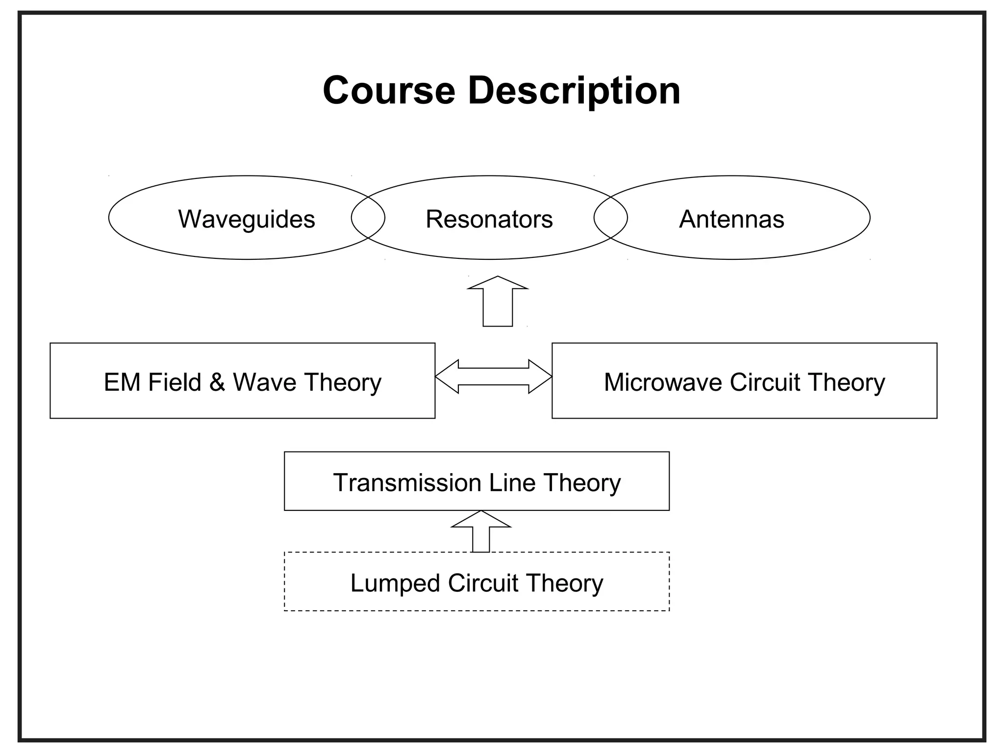
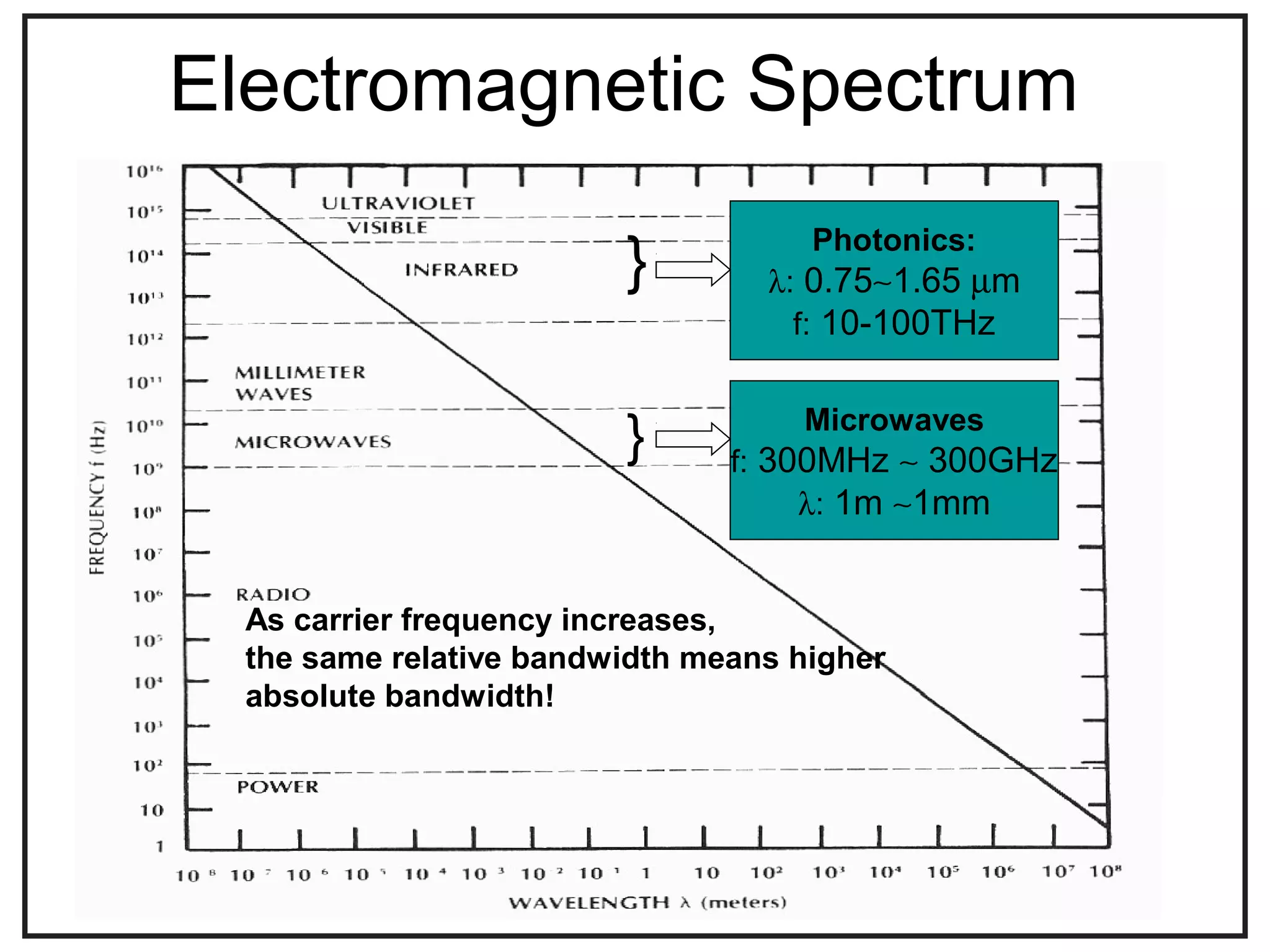
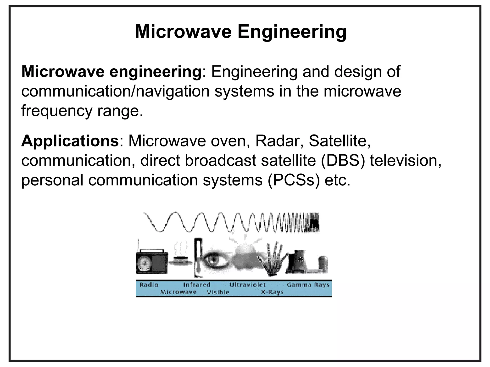
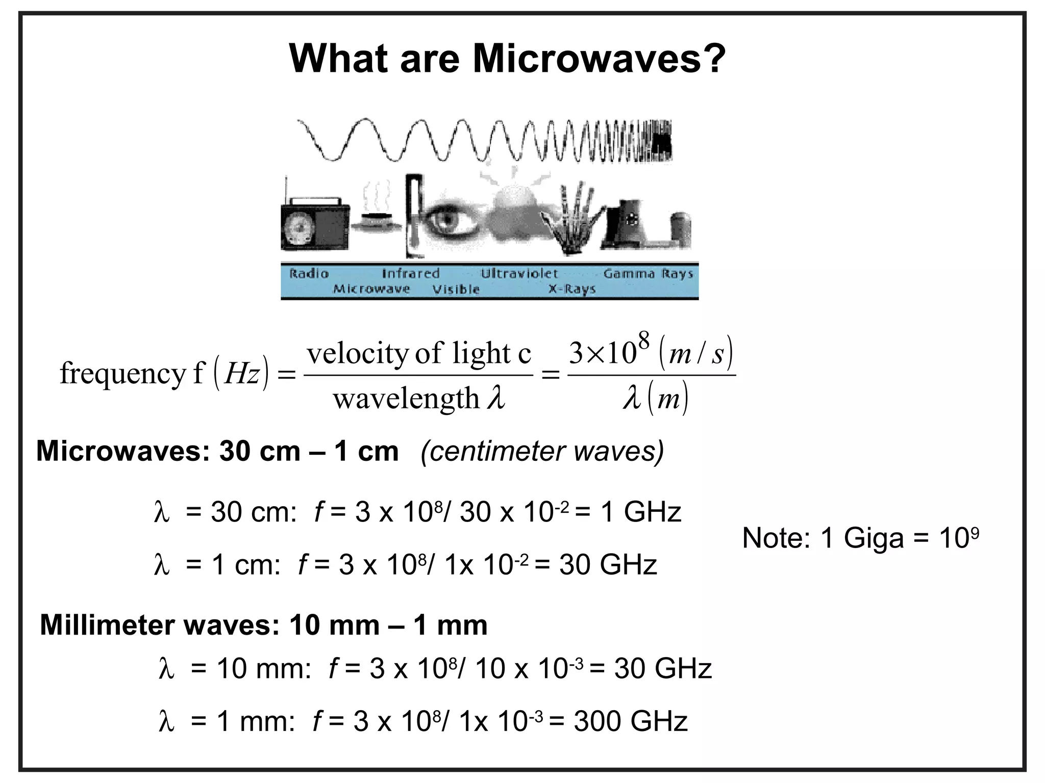
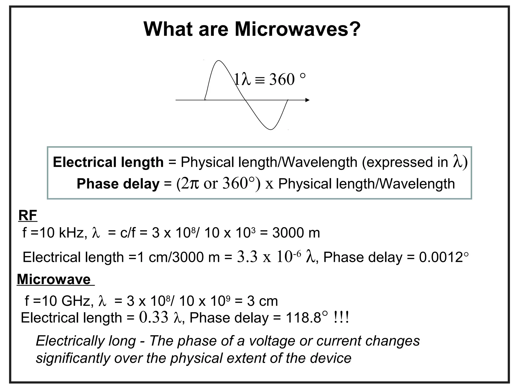
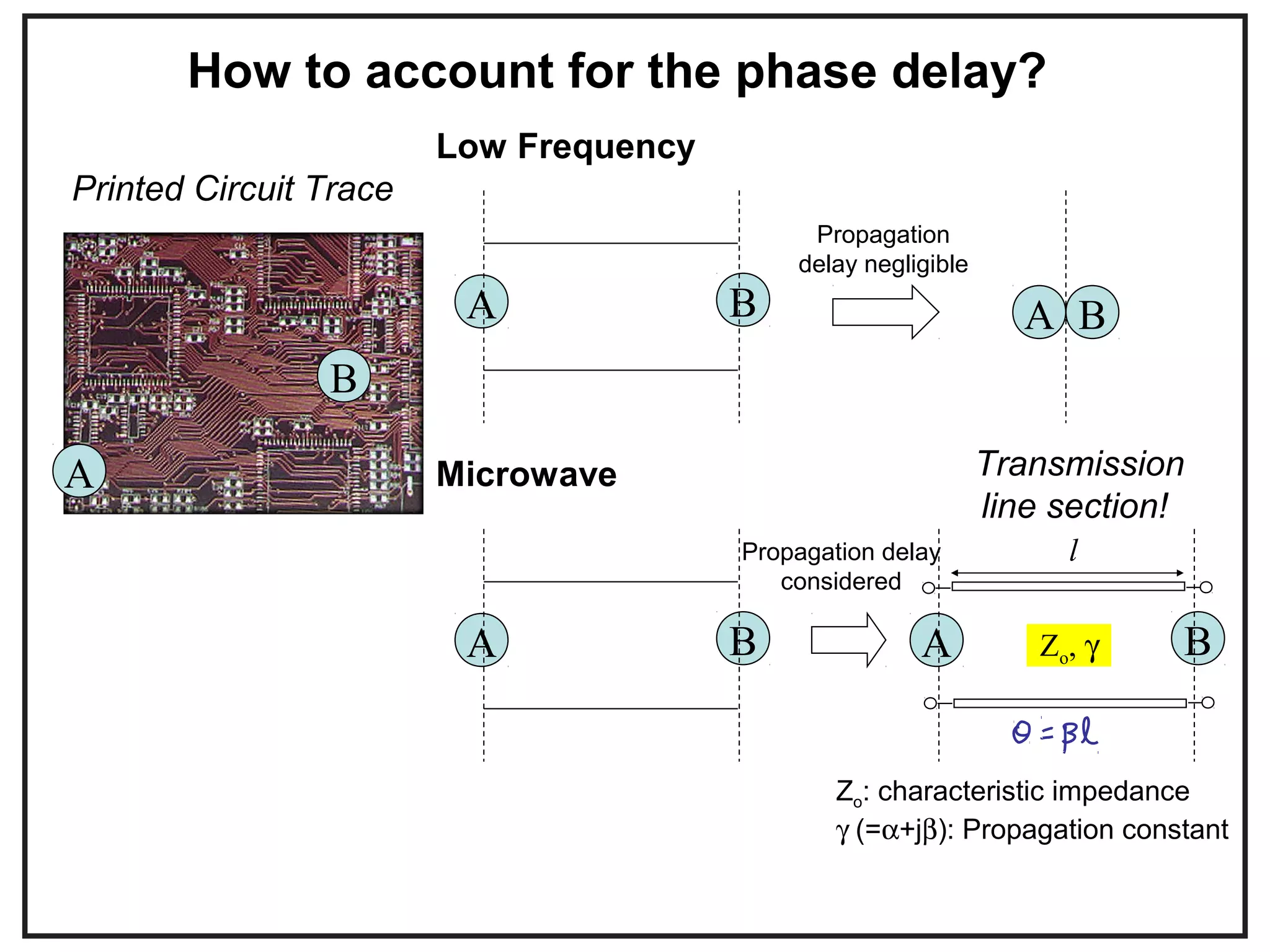
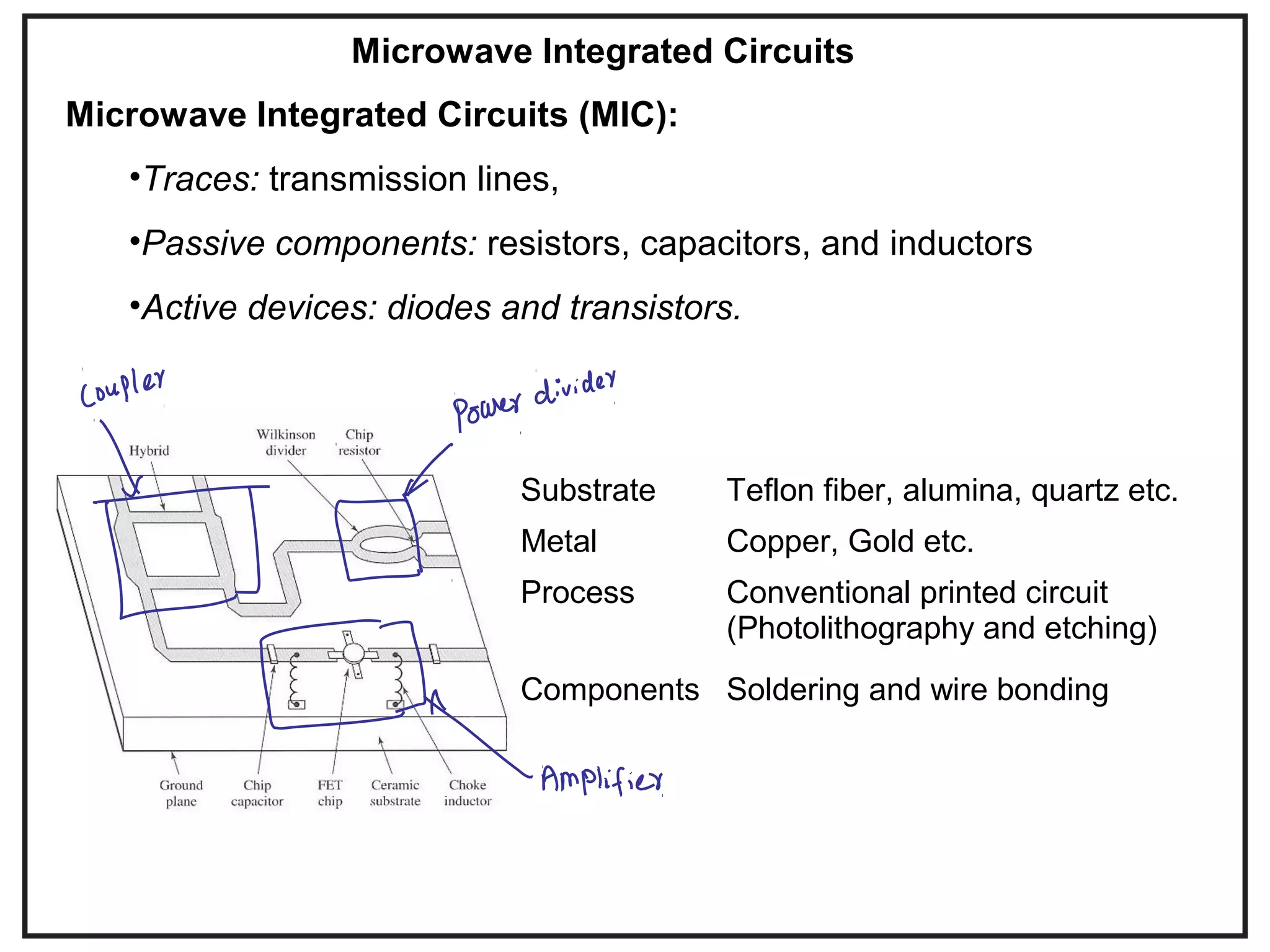
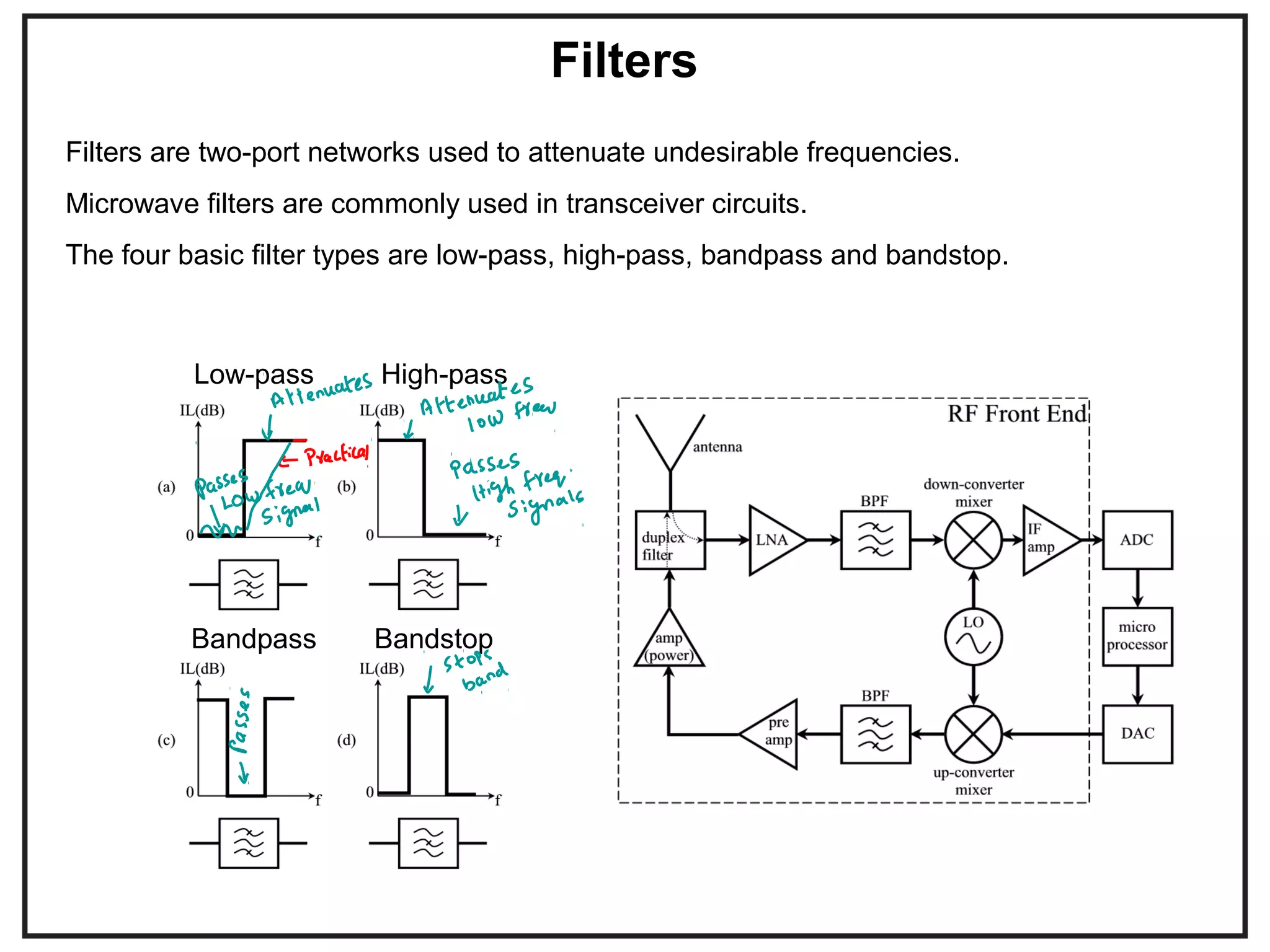
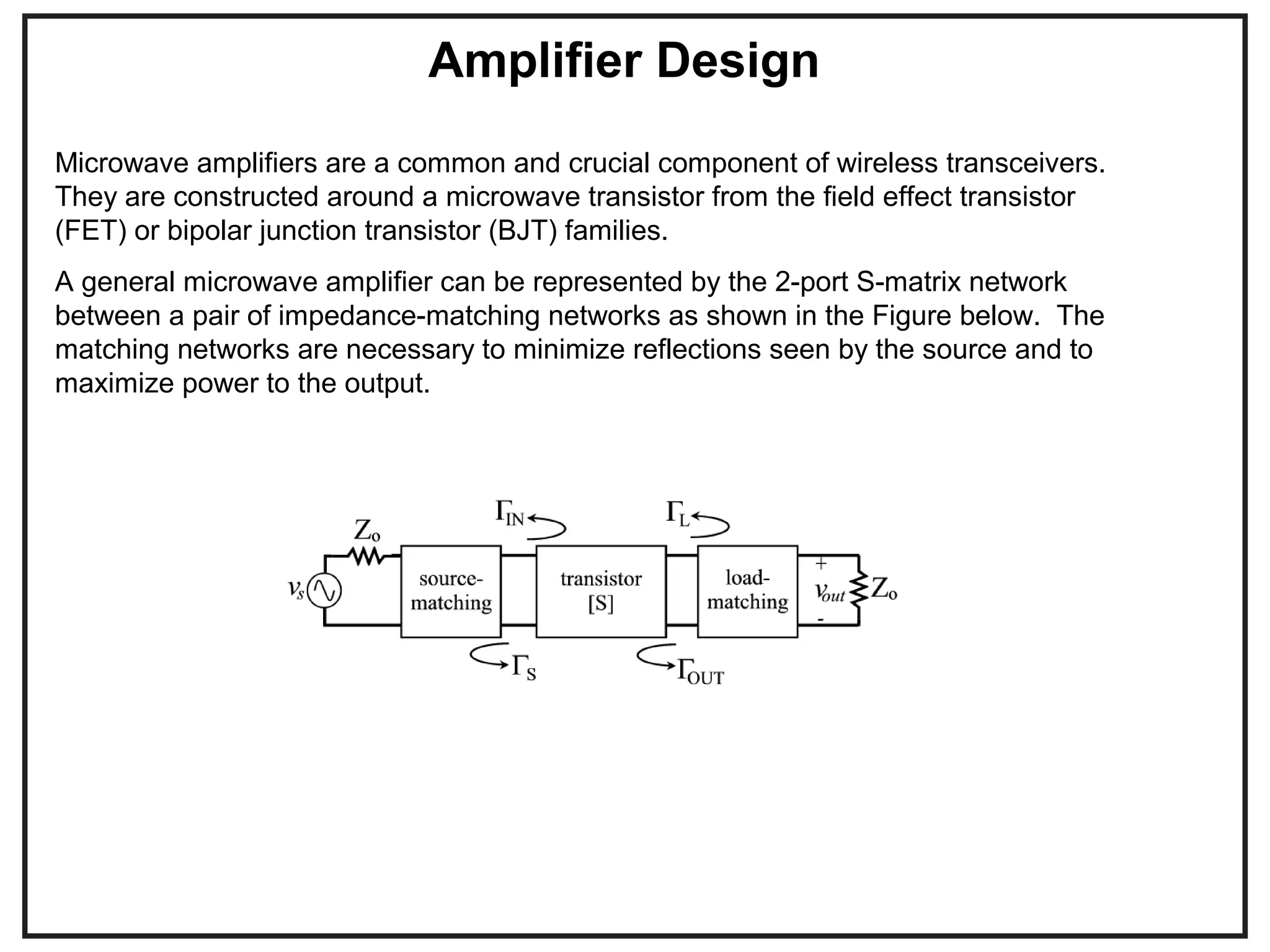
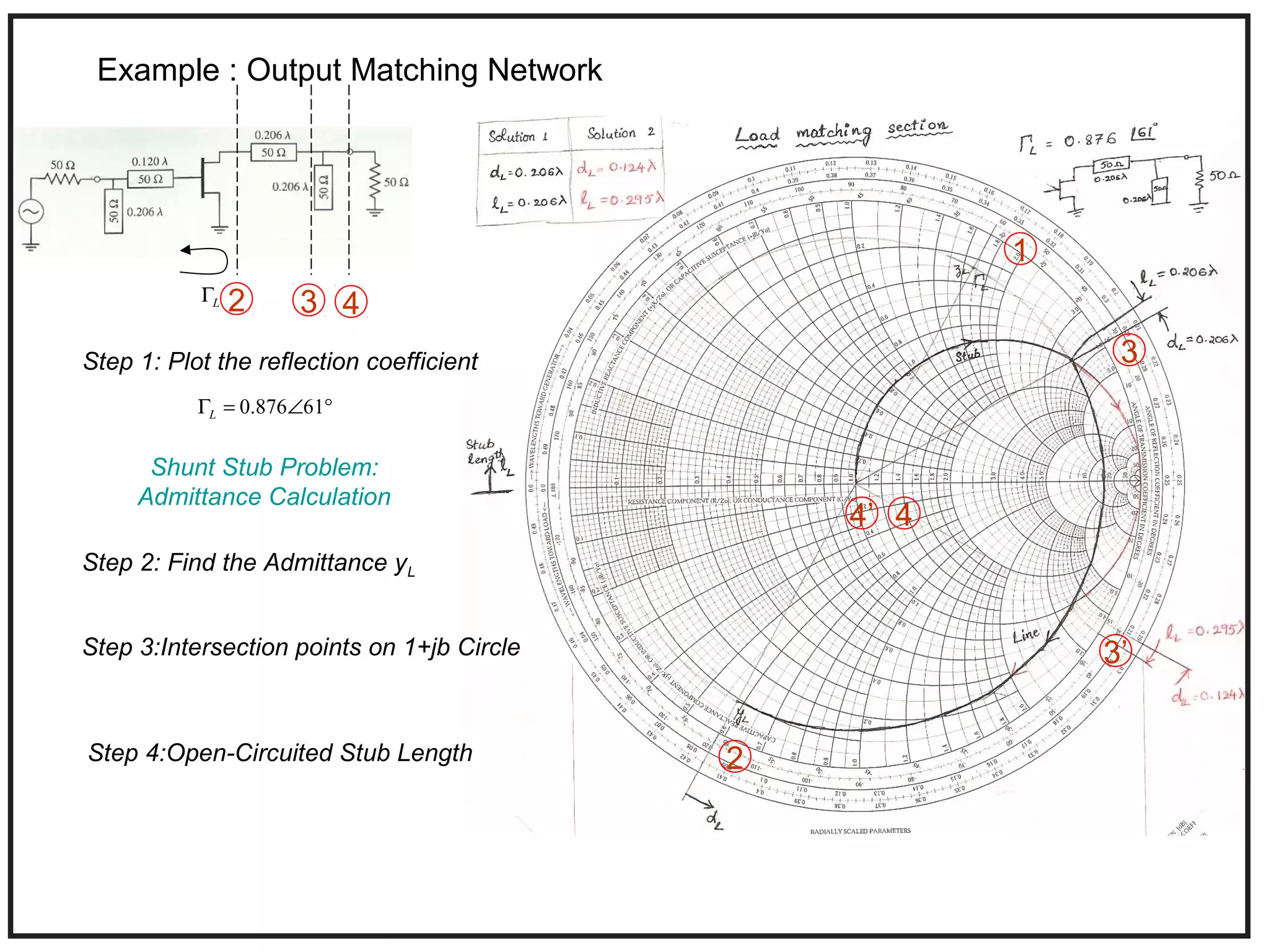
This document provides an overview of microwave engineering and describes key concepts such as transmission lines, scattering parameters, couplers, and filters. The objectives are to provide the basic theory of microwaves and examine applications in modern communication systems. Microwave engineering involves the design of systems like radar, satellite communications, and wireless networks that operate in the microwave frequency range from 300 MHz to 300 GHz.

![Scattering Parameters (S-Parameters)
•Consider a circuit or device inserted into a T-
Line as shown in the Figure.
•We can refer to this circuit or device as a
two-port network.
•The behavior of the network can be
completely characterized by its scattering
parameters (S-parameters), or its scattering
matrix, [S].
•Scattering matrices are frequently used to
characterize multiport networks, especially at
high frequencies.
•They are used to represent microwave
devices, such as amplifiers and circulators,
and are easily related to concepts of gain,
loss and reflection.
[ ] 11 12
21 22
S S
S
S S
=
Scattering matrix](https://image.slidesharecdn.com/introductiontomicrowaves-150628040624-lva1-app6891/75/Introduction-to-microwaves-11-2048.jpg)
![Scattering Parameters (S-Parameters)
The scattering parameters represent ratios of
voltage waves entering and leaving the ports
(If the same characteristic impedance, Zo, at
all ports in the network are the same).
1 11 1 12 2 .V S V S V− + +
= +
2 21 1 22 2
.V S V S V− + +
= +
11 121 1
21 222 2
,
S SV V
S SV V
− +
− +
=
In matrix form this is written
[ ] [ ][ ] .V S V
− +
=
2
1
11
1 0V
V
S
V +
−
+
=
=
1
1
12
2 0V
V
S
V +
−
+
=
=
1
2
22
2 0V
V
S
V +
−
+
=
=
2
2
21
1 0V
V
S
V +
−
+
=
=](https://image.slidesharecdn.com/introductiontomicrowaves-150628040624-lva1-app6891/75/Introduction-to-microwaves-12-2048.jpg)
![Scattering Parameters (S-Parameters)
Properties:
The two-port network is reciprocal if the
transmission characteristics are the same in
both directions (i.e. S21 = S12).
It is a property of passive circuits (circuits with
no active devices or ferrites) that they form
reciprocal networks.
A network is reciprocal if it is equal to its
transpose. Stated mathematically, for a
reciprocal network
[ ] [ ] ,
t
S S=
11 12 11 21
21 22 12 22
.
t
S S S S
S S S S
=
12 21S S=Condition for Reciprocity:
1) Reciprocity](https://image.slidesharecdn.com/introductiontomicrowaves-150628040624-lva1-app6891/75/Introduction-to-microwaves-13-2048.jpg)
![Scattering Parameters (S-Parameters)
Properties:
A lossless network does not contain any resistive
elements and there is no attenuation of the signal.
No real power is delivered to the network.
Consequently, for any passive lossless network,
what goes in must come out!
In terms of scattering parameters, a network is
lossless if
2) Lossless Networks
[ ] [ ] [ ]*
,
t
S S U=
1 0
[ ] .
0 1
U =
where [U] is the unitary matrix
For a 2-port network, the product of the transpose matrix and the complex conjugate
matrix yields
[ ] [ ]
( ) ( )
( ) ( )
2 2 * *
11 21 11 12 21 22*
2 2* *
12 11 22 21 12 22
1 0
0 1
t
S S S S S S
S S
S S S S S S
+ +
=
+ +
=
2 2
11 21
1S S+ =
If the network is reciprocal and lossless
* *
11 12 21 22
0S S S S+ =](https://image.slidesharecdn.com/introductiontomicrowaves-150628040624-lva1-app6891/75/Introduction-to-microwaves-14-2048.jpg)
![[ ]
−
−
=
00
00
00
00
αβ
αβ
βα
βα
S
[ ]
=
0
0
0
0
342414
342313
242312
141312
SSS
SSS
SSS
SSS
S
[ ]
=
00
00
00
00
αβ
αβ
βα
βα
j
j
j
j
S
SymmetricCoupler AntisymmetricCoupler
122
=+βα
Areciprocal,lossless,matchedfour-portnetwork
behavesasadirectionalcoupler
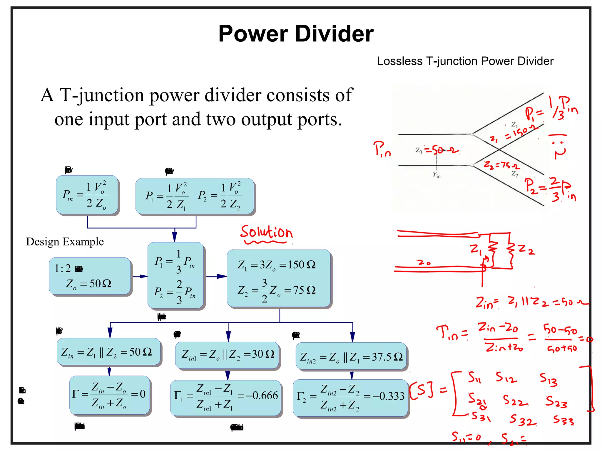
Couplers
COUPLERS
A coupler will transmit half or more of its
power from its input (port 1) to its through
port (port 2).
A portion of the power will be drawn off to
the coupled port (port 3), and ideally none
will go to the isolated port (port 4).
If the isolated port is internally terminated
in a matched load, the coupler is most
often referred to as a directional coupler.
For a lossless network:
Coupling coefficient: ( )3120log .C S= −
( )2120log .IL S= −Insertion Loss:
( )4120log ,I S= −Isolation:
31
41
20log ,
S
D
S
=
÷
Directivity:
(dB)D I C= −](https://image.slidesharecdn.com/introductiontomicrowaves-150628040624-lva1-app6891/75/Introduction-to-microwaves-20-2048.jpg)
![COUPLERS
Design Example
Example 10.10: Suppose an antisymmetrical coupler has the following characteristics:
C = 10.0 dB
D = 15.0 dB
IL = 2.00 dB
VSWR = 1.30
Coupling coefficient: ( )3120log .C S= −
( )2120log .IL S= −Insertion Loss:
10/ 20
31 10 0.316.S −
= =
2 / 20
21 10 0.794.S −
= =
11
1
0.130.
1
VSWR
S
VSWR
−
= =
+
25 ,I D C dB= + =
25/ 20
41 10 0.056.S −
= =
VSWR = 1.30
[ ]
0.130 0.794 0.316 0.056
0.794 0.130 0.056 0.316
0.316 0.056 0.130 0.794
0.056 0.316 0.794 0.130
S
−
=
−
Given](https://image.slidesharecdn.com/introductiontomicrowaves-150628040624-lva1-app6891/75/Introduction-to-microwaves-21-2048.jpg)
![COUPLERS
[ ]
0 1 1 0
1 0 0 1
.
1 0 0 12
0 1 1 0
j
S
−−
=
−
[ ]
0 1 0
0 0 11
1 0 02
0 1 0
,
j
j
S
j
j
−
=
The quadrature hybrid (or branch-line hybrid) is
a 3 dB coupler. The quadrature term comes
from the 90 deg phase difference between the
outputs at ports 2 and 3.
The coupling and insertion loss are both equal
to 3 dB.
Ring hybrid (or rat-race) couplerQuadrature hybrid Coupler
A microwave signal fed at port 1 will split evenly
in both directions, giving identical signals out of
ports 2 and 3. But the split signals are 180 deg
out of phase at port 4, the isolated port, so they
cancel and no power exits port 4.
The insertion loss and coupling are both equal to
3 dB. Not only can the ring hybrid split power to
two ports, but it can add and subtract a pair of
signals.](https://image.slidesharecdn.com/introductiontomicrowaves-150628040624-lva1-app6891/75/Introduction-to-microwaves-22-2048.jpg)


![RF Circuit Design - [Ch3-1] Microwave Network](https://cdn.slidesharecdn.com/ss_thumbnails/ch3-1-150613064402-lva1-app6892-thumbnail.jpg?width=640&height=640&fit=bounds)


