Downloaded 371 times

![Department of Electronic Engineering, NTUT
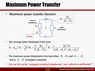
Normalized Impedances (I)
Reference:
[1] K. Kurokawa, “Power waves and the scattering matrix.” IEEE Trans. Microwave Theory and techniques, vol. 13, pp.194-202,
Mar. 1965.
LZ
sE
sZ
V
I
s s sZ R jX
L L LZ R jX
• Normalize the impedances with respect to Rs
1 s
s s s
s
X
z r jx j
R
L L
L L L
s s
R X
z r jx j
R R
4/31](https://image.slidesharecdn.com/ch3-2-150613064404-lva1-app6891/85/RF-Circuit-Design-Ch3-2-Power-Waves-and-Power-Gain-Expressions-4-320.jpg)
![Department of Electronic Engineering, NTUT
Generalized Scattering Parameter (I)
1 11 1 12 2p p p p pb S a S a
2 21 1 22 2p p p p pb S a S a
1 1 1 1
1
1
2
pa V Z I
R
2 2 2 2
2
1
2
pa V Z I
R
1 1 1 1
1
1
2
pb V Z I
R
Two-port
Network
[Sp]
2pa
2pb
1pa
1pb
Port 1 Port 2
1E
1Z
2I1I
1V
2V
2E
2Z
1 2 2 2
2
1
2
pb V Z I
R
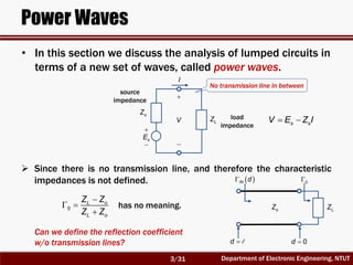
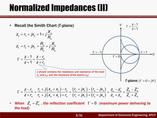
• Considering a two-port network, the generalized scattering matrix [Sp]
is found with respect to a reference impedance Re{Z1} at port 1 and
to Re{Z2} at port 2. If Z1 = Z2 = Zo, [Sp] = [S].
9/31](https://image.slidesharecdn.com/ch3-2-150613064404-lva1-app6891/85/RF-Circuit-Design-Ch3-2-Power-Waves-and-Power-Gain-Expressions-9-320.jpg)
![Department of Electronic Engineering, NTUT
Generalized Scattering Parameter (II)
2
1
11
1 0p
p
p
p a
b
S
a
Two-port
Network
[Sp]
2 0pa
2pb
1pa
1pb
Port 1 Port 2
1E
1Z
2I1I
1V
2V
2Z
1 11 1 12 2p p p p pb S a S a
2 21 1 22 2p p p p pb S a S a
1 1
11
1 1
T
p
T
Z Z
S
Z Z
2 2 2
1 1 11
1 1
1
2 2
IN p p AVS pP a b P S
1TZ
• Can we find the power by using [S] but not [Sp] ? Sure! We will talk
about this later.
10/31](https://image.slidesharecdn.com/ch3-2-150613064404-lva1-app6891/85/RF-Circuit-Design-Ch3-2-Power-Waves-and-Power-Gain-Expressions-10-320.jpg)
![Department of Electronic Engineering, NTUT
Power-Gain Expressions (I)
Transistor
[S]
2a
2b
1a
1b
Port 1 Port 2
sE
sZ
out
LZ
in
s L
s o
s
s o
Z Z
Z Z
L o
L
L o
Z Z
Z Z
1 11 1 12 2b S a S a
2 21 1 22 2b S a S a
• Consider a microwave amplifier with the source and load reflection
coefficients and measured in a Zo system:s L
• For the transistor, the input and output traveling waves measured in a
Zo system (this is very practical) :
14/31](https://image.slidesharecdn.com/ch3-2-150613064404-lva1-app6891/85/RF-Circuit-Design-Ch3-2-Power-Waves-and-Power-Gain-Expressions-14-320.jpg)
![Department of Electronic Engineering, NTUT
Power-Gain Expressions (II)
sE
sZ
s
LZ
L
Transistor
[S]
The reflection coefficients and S-parameters are separately measured
in a Zo (usually 50 Ω) system
Transistor
[S]
2a
2b
1a
1b
sE
sZ
out
LZ
in
s L
After connecting them all together
The goal is to find the input and output
power relations.
1b
1a 2a
2b
15/31](https://image.slidesharecdn.com/ch3-2-150613064404-lva1-app6891/85/RF-Circuit-Design-Ch3-2-Power-Waves-and-Power-Gain-Expressions-15-320.jpg)
![Department of Electronic Engineering, NTUT
Input Reflection Coefficient
1
1
in
b
a
2 2La b
2 21 1 22 2Lb S a S b 21 1
2
221 L
S a
b
S
Transistor
[S]
2a
2b
1a
1b
sE
sZ
out
LZ
in
s L
• After connecting the circuits together, the first step is to find the new
input coefficient , which is the result coming from and .in S L
1 11 1 12 2b S a S a
2 21 1 22 2b S a S a
1 12 21
11
1 221
L
in
L
b S S
S
a S
12 21
1 11 1 12 2 11 1 1
221
L
L
L
S S
b S a S b S a a
S
a1 is your input, so the goal here is to find the reflected wave b1
1 11 1 12 2b S a S a
a1 is your input, to find b1 = you need to find a2
to find a2 = you need to find b2
the relationship between b2 and a1
16/31](https://image.slidesharecdn.com/ch3-2-150613064404-lva1-app6891/85/RF-Circuit-Design-Ch3-2-Power-Waves-and-Power-Gain-Expressions-16-320.jpg)
![Department of Electronic Engineering, NTUT
Output Reflection Coefficient
2
2 0s
out
E
b
a
1 1sa b
1 11 1 12 2sb S b S a 12 2
1
111 s
S a
b
S
12 21
2 21 1 22 2 2 22 2
111
s
s
s
S S
b S b S a a S a
S
12 212
22
2 110
1
s
s
out
sE
S Sb
S
a S
Transistor
[S]
2a
2b
1a
1b
sE
sZ
out
LZ
in
s L
• After connecting the circuits together, the second step is to find the
new output coefficient , which is the result coming from and .out S s
1 11 1 12 2b S a S a
2 21 1 22 2b S a S a
The same procedure as finding is applied.in
17/31](https://image.slidesharecdn.com/ch3-2-150613064404-lva1-app6891/85/RF-Circuit-Design-Ch3-2-Power-Waves-and-Power-Gain-Expressions-17-320.jpg)
![Department of Electronic Engineering, NTUT
Definition of the Power Gains
Transistor
[S]
sE
sZ
LZ
PAVNPAVS PLPin
Ms
interface interface
ML
• The power gain L
p
in
P
G
P
• The transducer power gain L
T p s
AVS
P
G G M
P
• The available power gain AVN T
A
AVS L
P G
G
P M
p TG G
A TG G
• When the Input and output are matched: p T AG G G
From the amplifier input to load
From the source to load
21/31](https://image.slidesharecdn.com/ch3-2-150613064404-lva1-app6891/85/RF-Circuit-Design-Ch3-2-Power-Waves-and-Power-Gain-Expressions-21-320.jpg)
![Department of Electronic Engineering, NTUT
Power Gain
2 2
2
2 2
1
1
1
2
1
1
2
L
L
p
in
in
bP
G
P a
21 1
2
221 L
S a
b
S
2
2
212 2
22
11
1 1
L
p
in L
G S
S
• The Power Gain Gp
where
Transistor
[S]
sE
sZ
LZ
PAVNPAVS PLPin
Ms
interface interface
ML
22/31](https://image.slidesharecdn.com/ch3-2-150613064404-lva1-app6891/85/RF-Circuit-Design-Ch3-2-Power-Waves-and-Power-Gain-Expressions-22-320.jpg)
![Department of Electronic Engineering, NTUT
Transducer Power Gain
• The Transducer Power Gain GT
L L in in
T p p s
AVS in AVS AVS
P P P P
G G G M
P P P P
2 2 2 2
2 2
21 212 2 2 2
22 11
1 1 1 1
1 1 1 1
s L s L
T
s in L s out L
G S S
S S
2 2
2
1 1
1
s in
s
s in
M
where
Transistor
[S]
sE
sZ
LZ
PAVNPAVS PLPin
Ms
interface interface
ML
23/31](https://image.slidesharecdn.com/ch3-2-150613064404-lva1-app6891/85/RF-Circuit-Design-Ch3-2-Power-Waves-and-Power-Gain-Expressions-23-320.jpg)
![Department of Electronic Engineering, NTUT
Available Power Gain
• The Available Power Gain GA
AVN L AVN AVN T
A T
AVS AVS L L L
P P P P G
G G
P P P P M
2
2
212 2
11
1 1
1 1
s
A
s out
G S
S
Transistor
[S]
sE
sZ
LZ
PAVNPAVS PLPin
Ms
interface interface
ML
2 2
2
1 1
1
L out
L
out L
M
where
24/31](https://image.slidesharecdn.com/ch3-2-150613064404-lva1-app6891/85/RF-Circuit-Design-Ch3-2-Power-Waves-and-Power-Gain-Expressions-24-320.jpg)
![Department of Electronic Engineering, NTUT
Summary
• The power delivered to the load can be calculated by using three
methods:
(1) Real power dissipated at load ( )
(2) Power waves (generalized [Sp], linked with reflections)
(3) Traveling waves ([S], it’s practical and useful in amplifier design)
Re 2L L LP V I
• Available power from source (maximum average power the source can
provide when matched) :
2
2 2
,
1
2 8
s
AVS p p rms
s
E
P a a
R
2 2 21 1 1
2 2 2
L p p AVS pP a b P b
• When mismatch occurs:
Power wave
Power wave
L p inP G P L T AVSP G P
• Power gains (defined with traveling waves, circuitries are separately
measured in a Zo system) :
31/31](https://image.slidesharecdn.com/ch3-2-150613064404-lva1-app6891/85/RF-Circuit-Design-Ch3-2-Power-Waves-and-Power-Gain-Expressions-31-320.jpg)

El capítulo 3-2 discute la transferencia máxima de potencia y las expresiones de ganancia de potencia mediante el análisis de circuitos agrupados en el contexto de ondas de potencia. Se aborda cómo definir coeficientes de reflexión y el teorema de conjugación en circuitos sin línea de transmisión, así como las implicaciones de la adaptación de impedancias. También se presentan ejemplos de cálculo de ondas de potencia y parámetros de dispersión en redes de dos puertos.

![RF Circuit Design - [Ch1-2] Transmission Line Theory](https://cdn.slidesharecdn.com/ss_thumbnails/ch1-2-150613064349-lva1-app6892-thumbnail.jpg?width=640&height=640&fit=bounds)
![RF Circuit Design - [Ch2-2] Smith Chart](https://cdn.slidesharecdn.com/ss_thumbnails/ch2-2-150613064401-lva1-app6891-thumbnail.jpg?width=640&height=640&fit=bounds)
![RF Circuit Design - [Ch3-1] Microwave Network](https://cdn.slidesharecdn.com/ss_thumbnails/ch3-1-150613064402-lva1-app6892-thumbnail.jpg?width=640&height=640&fit=bounds)
![RF Circuit Design - [Ch4-1] Microwave Transistor Amplifier](https://cdn.slidesharecdn.com/ss_thumbnails/ch4-1-150613064409-lva1-app6892-thumbnail.jpg?width=640&height=640&fit=bounds)
![RF Circuit Design - [Ch2-1] Resonator and Impedance Matching](https://cdn.slidesharecdn.com/ss_thumbnails/ch2-1-150613064353-lva1-app6892-thumbnail.jpg?width=640&height=640&fit=bounds)
![RF Module Design - [Chapter 3] Linearity](https://cdn.slidesharecdn.com/ss_thumbnails/rfch3-150613070345-lva1-app6891-thumbnail.jpg?width=640&height=640&fit=bounds)
![RF Module Design - [Chapter 1] From Basics to RF Transceivers](https://cdn.slidesharecdn.com/ss_thumbnails/rfch1-150613070344-lva1-app6892-thumbnail.jpg?width=640&height=640&fit=bounds)
![Circuit Network Analysis - [Chapter1] Basic Circuit Laws](https://cdn.slidesharecdn.com/ss_thumbnails/ch1-150613063856-lva1-app6892-thumbnail.jpg?width=640&height=640&fit=bounds)
![RF Module Design - [Chapter 6] Power Amplifier](https://cdn.slidesharecdn.com/ss_thumbnails/rfch6-150613070347-lva1-app6891-thumbnail.jpg?width=640&height=640&fit=bounds)
![射頻電子 - [第三章] 史密斯圖與阻抗匹配](https://cdn.slidesharecdn.com/ss_thumbnails/ch3-150613065103-lva1-app6892-thumbnail.jpg?width=640&height=640&fit=bounds)
![射頻電子 - [第五章] 射頻放大器設計](https://cdn.slidesharecdn.com/ss_thumbnails/ch5-150613065105-lva1-app6892-thumbnail.jpg?width=640&height=640&fit=bounds)
![RF Circuit Design - [Ch4-2] LNA, PA, and Broadband Amplifier](https://cdn.slidesharecdn.com/ss_thumbnails/ch4-2-150613064410-lva1-app6891-thumbnail.jpg?width=640&height=640&fit=bounds)
![Agilent ADS 模擬手冊 [實習2] 放大器設計](https://cdn.slidesharecdn.com/ss_thumbnails/2adsamp-150613072818-lva1-app6892-thumbnail.jpg?width=640&height=640&fit=bounds)
![Circuit Network Analysis - [Chapter2] Sinusoidal Steady-state Analysis](https://cdn.slidesharecdn.com/ss_thumbnails/ch2-150613063856-lva1-app6892-thumbnail.jpg?width=640&height=640&fit=bounds)
![射頻電子 - [第一章] 知識回顧與通訊系統簡介](https://cdn.slidesharecdn.com/ss_thumbnails/ch1-150613065058-lva1-app6891-thumbnail.jpg?width=640&height=640&fit=bounds)

![RF Module Design - [Chapter 5] Low Noise Amplifier](https://cdn.slidesharecdn.com/ss_thumbnails/rfch5-150613070346-lva1-app6891-thumbnail.jpg?width=640&height=640&fit=bounds)
![射頻電子實驗手冊 [實驗1 ~ 5] ADS入門, 傳輸線模擬, 直流模擬, 暫態模擬, 交流模擬](https://cdn.slidesharecdn.com/ss_thumbnails/simlab15-150613072411-lva1-app6892-thumbnail.jpg?width=640&height=640&fit=bounds)
![RF Module Design - [Chapter 8] Phase-Locked Loops](https://cdn.slidesharecdn.com/ss_thumbnails/rfch8-150613070348-lva1-app6892-thumbnail.jpg?width=640&height=640&fit=bounds)

![Multiband Transceivers - [Chapter 2] Noises and Linearities](https://cdn.slidesharecdn.com/ss_thumbnails/ch2-150613070933-lva1-app6892-thumbnail.jpg?width=640&height=640&fit=bounds)
![RF Circuit Design - [Ch1-1] Sinusoidal Steady-state Analysis](https://cdn.slidesharecdn.com/ss_thumbnails/ch1-1-150613064348-lva1-app6891-thumbnail.jpg?width=640&height=640&fit=bounds)
![RF Module Design - [Chapter 2] Noises](https://cdn.slidesharecdn.com/ss_thumbnails/rfch2-150613070344-lva1-app6892-thumbnail.jpg?width=640&height=640&fit=bounds)


![射頻電子實驗手冊 - [實驗7] 射頻放大器模擬](https://cdn.slidesharecdn.com/ss_thumbnails/simlab7-150613072420-lva1-app6892-thumbnail.jpg?width=640&height=640&fit=bounds)
![射頻電子 - [第二章] 傳輸線理論](https://cdn.slidesharecdn.com/ss_thumbnails/ch2-150613065059-lva1-app6891-thumbnail.jpg?width=640&height=640&fit=bounds)
![Circuit Network Analysis - [Chapter4] Laplace Transform](https://cdn.slidesharecdn.com/ss_thumbnails/ch4-150613063858-lva1-app6891-thumbnail.jpg?width=640&height=640&fit=bounds)
![電路學 - [第五章] 一階RC/RL電路](https://cdn.slidesharecdn.com/ss_thumbnails/circuitch5-150613063008-lva1-app6891-thumbnail.jpg?width=640&height=640&fit=bounds)
![射頻電子 - [第四章] 散射參數網路](https://cdn.slidesharecdn.com/ss_thumbnails/ch4-150613065103-lva1-app6891-thumbnail.jpg?width=640&height=640&fit=bounds)
![電路學 - [第六章] 二階RLC電路](https://cdn.slidesharecdn.com/ss_thumbnails/circuitch6-150613063009-lva1-app6892-thumbnail.jpg?width=640&height=640&fit=bounds)
![電路學 - [第七章] 正弦激勵, 相量與穩態分析](https://cdn.slidesharecdn.com/ss_thumbnails/circuitch7-150613063009-lva1-app6891-thumbnail.jpg?width=640&height=640&fit=bounds)
![電路學 - [第八章] 磁耦合電路](https://cdn.slidesharecdn.com/ss_thumbnails/circuitch8-150613063010-lva1-app6892-thumbnail.jpg?width=640&height=640&fit=bounds)
![Circuit Network Analysis - [Chapter3] Fourier Analysis](https://cdn.slidesharecdn.com/ss_thumbnails/ch3-150613063858-lva1-app6891-thumbnail.jpg?width=640&height=640&fit=bounds)
![Circuit Network Analysis - [Chapter5] Transfer function, frequency response, ...](https://cdn.slidesharecdn.com/ss_thumbnails/ch5-150613063859-lva1-app6891-thumbnail.jpg?width=640&height=640&fit=bounds)
![電路學 - [第四章] 儲能元件](https://cdn.slidesharecdn.com/ss_thumbnails/circuitch4-150613063008-lva1-app6891-thumbnail.jpg?width=640&height=640&fit=bounds)
![電路學 - [第三章] 網路定理](https://cdn.slidesharecdn.com/ss_thumbnails/circuitch3-150613063007-lva1-app6892-thumbnail.jpg?width=640&height=640&fit=bounds)
![射頻電子 - [第六章] 低雜訊放大器設計](https://cdn.slidesharecdn.com/ss_thumbnails/ch6-150613065106-lva1-app6892-thumbnail.jpg?width=640&height=640&fit=bounds)
![射頻電子 - [實驗第一章] 基頻放大器設計](https://cdn.slidesharecdn.com/ss_thumbnails/e1-150613065108-lva1-app6892-thumbnail.jpg?width=640&height=640&fit=bounds)


![Agilent ADS 模擬手冊 [實習3] 壓控振盪器模擬](https://cdn.slidesharecdn.com/ss_thumbnails/3adsosc-150613072819-lva1-app6892-thumbnail.jpg?width=640&height=640&fit=bounds)
![Agilent ADS 模擬手冊 [實習1] 基本操作與射頻放大器設計](https://cdn.slidesharecdn.com/ss_thumbnails/1adsbasics-150613072812-lva1-app6891-thumbnail.jpg?width=640&height=640&fit=bounds)
![射頻電子實驗手冊 - [實驗8] 低雜訊放大器模擬](https://cdn.slidesharecdn.com/ss_thumbnails/simlab8-150613072425-lva1-app6891-thumbnail.jpg?width=640&height=640&fit=bounds)
![射頻電子實驗手冊 [實驗6] 阻抗匹配模擬](https://cdn.slidesharecdn.com/ss_thumbnails/simlab6-150613072411-lva1-app6892-thumbnail.jpg?width=640&height=640&fit=bounds)
![[ZigBee 嵌入式系統] ZigBee Architecture 與 TI Z-Stack Firmware](https://cdn.slidesharecdn.com/ss_thumbnails/zigbeearchitecture-150613072045-lva1-app6892-thumbnail.jpg?width=640&height=640&fit=bounds)
![[ZigBee 嵌入式系統] ZigBee 應用實作 - 使用 TI Z-Stack Firmware](https://cdn.slidesharecdn.com/ss_thumbnails/zigbeeappimplementation-150613072040-lva1-app6891-thumbnail.jpg?width=640&height=640&fit=bounds)
![[嵌入式系統] MCS-51 實驗 - 使用 IAR (3)](https://cdn.slidesharecdn.com/ss_thumbnails/mcs51iarpart3-150613071723-lva1-app6892-thumbnail.jpg?width=640&height=640&fit=bounds)
![[嵌入式系統] MCS-51 實驗 - 使用 IAR (2)](https://cdn.slidesharecdn.com/ss_thumbnails/mcs51iarpart2-150613071717-lva1-app6891-thumbnail.jpg?width=640&height=640&fit=bounds)
![[嵌入式系統] MCS-51 實驗 - 使用 IAR (1)](https://cdn.slidesharecdn.com/ss_thumbnails/mcs51iarpart1-150613071712-lva1-app6892-thumbnail.jpg?width=640&height=640&fit=bounds)

![[嵌入式系統] 嵌入式系統進階](https://cdn.slidesharecdn.com/ss_thumbnails/advembedded-150613071653-lva1-app6892-thumbnail.jpg?width=640&height=640&fit=bounds)
![Multiband Transceivers - [Chapter 7] Spec. Table](https://cdn.slidesharecdn.com/ss_thumbnails/ch7table-150613070936-lva1-app6892-thumbnail.jpg?width=640&height=640&fit=bounds)
![Multiband Transceivers - [Chapter 7] Multi-mode/Multi-band GSM/GPRS/TDMA/AMP...](https://cdn.slidesharecdn.com/ss_thumbnails/ch7-150613070936-lva1-app6892-thumbnail.jpg?width=640&height=640&fit=bounds)
![Multiband Transceivers - [Chapter 6] Multi-mode and Multi-band Transceivers](https://cdn.slidesharecdn.com/ss_thumbnails/ch6-150613070935-lva1-app6891-thumbnail.jpg?width=640&height=640&fit=bounds)
![Multiband Transceivers - [Chapter 4] Design Parameters of Wireless Radios](https://cdn.slidesharecdn.com/ss_thumbnails/ch4-150613070934-lva1-app6892-thumbnail.jpg?width=640&height=640&fit=bounds)
![Multiband Transceivers - [Chapter 5] Software-Defined Radios](https://cdn.slidesharecdn.com/ss_thumbnails/ch5-150613070934-lva1-app6892-thumbnail.jpg?width=640&height=640&fit=bounds)


