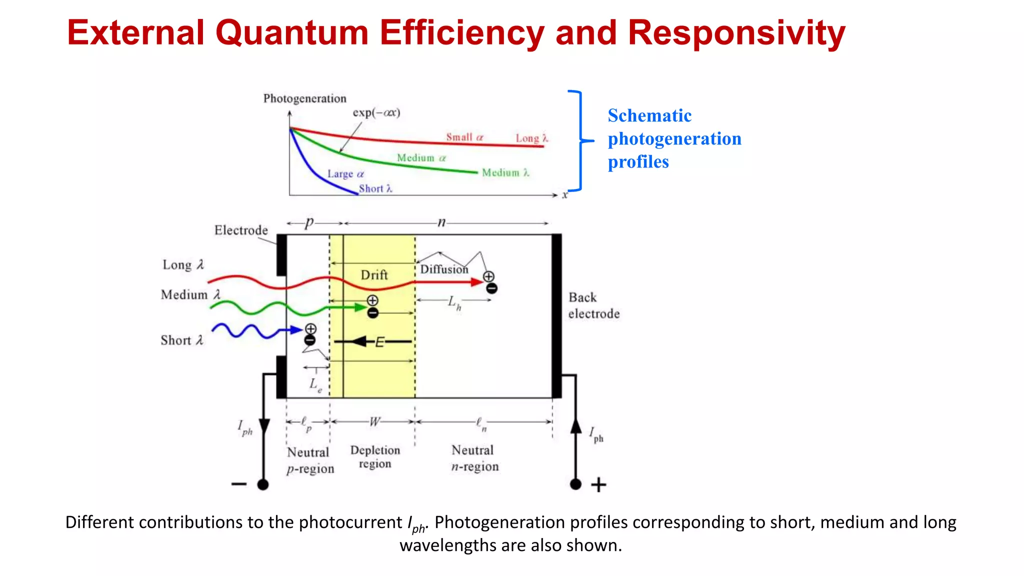
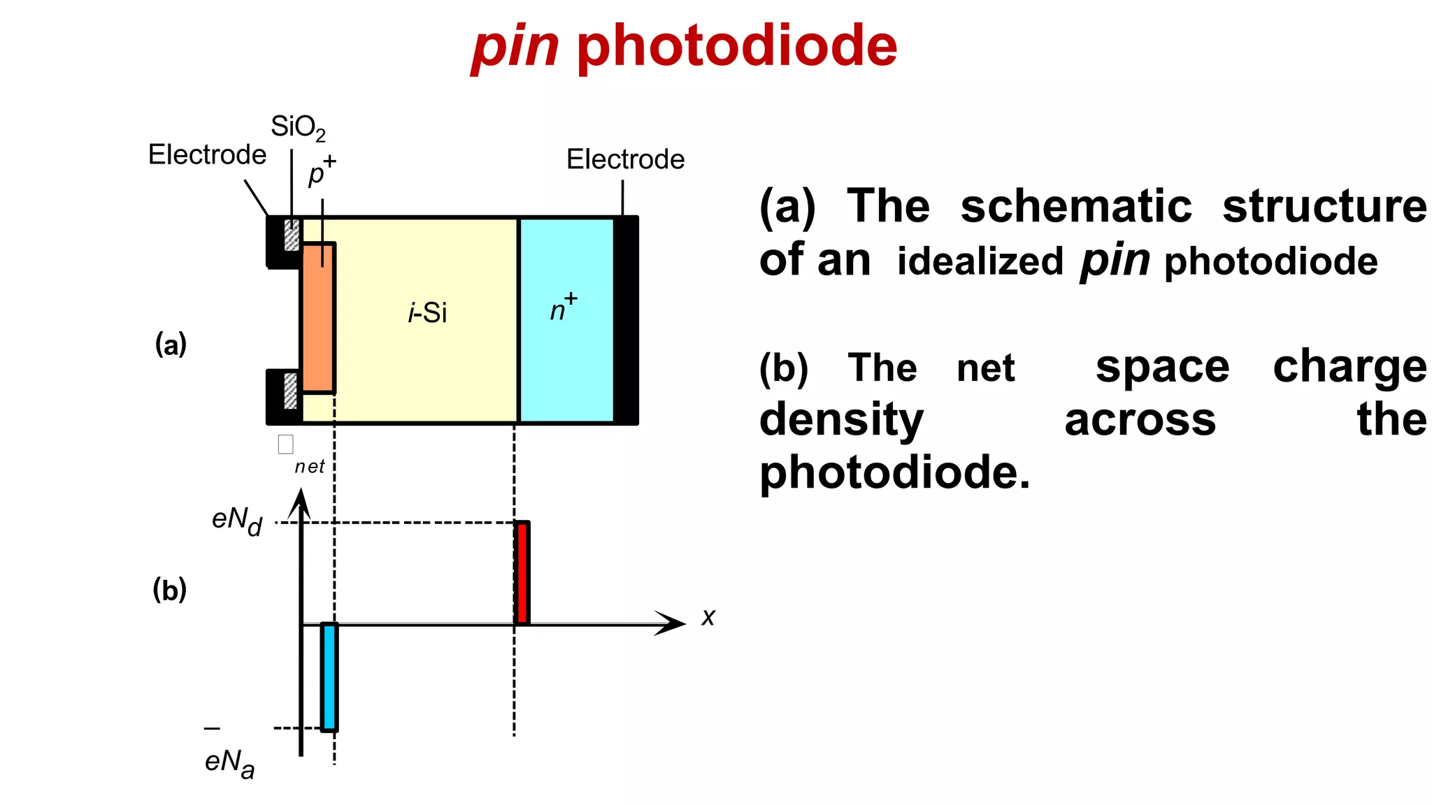
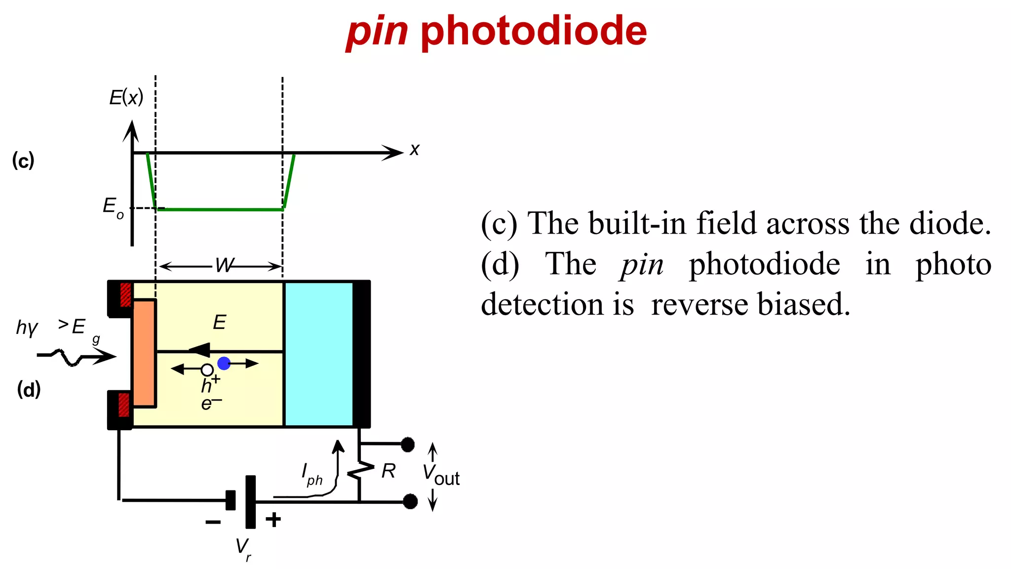
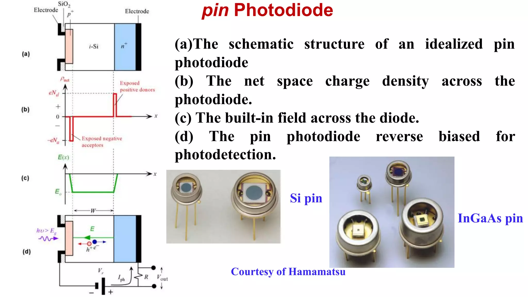
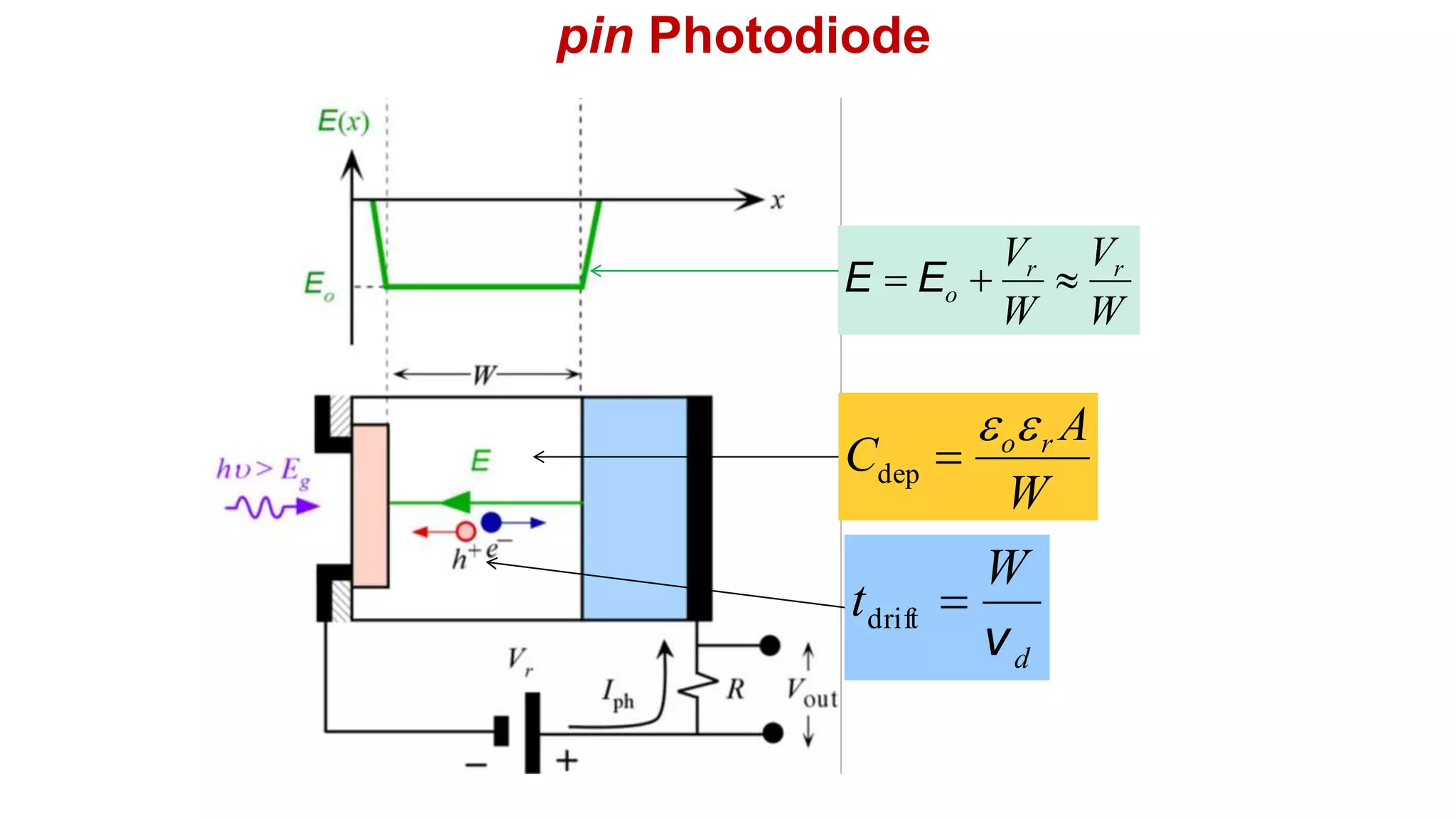
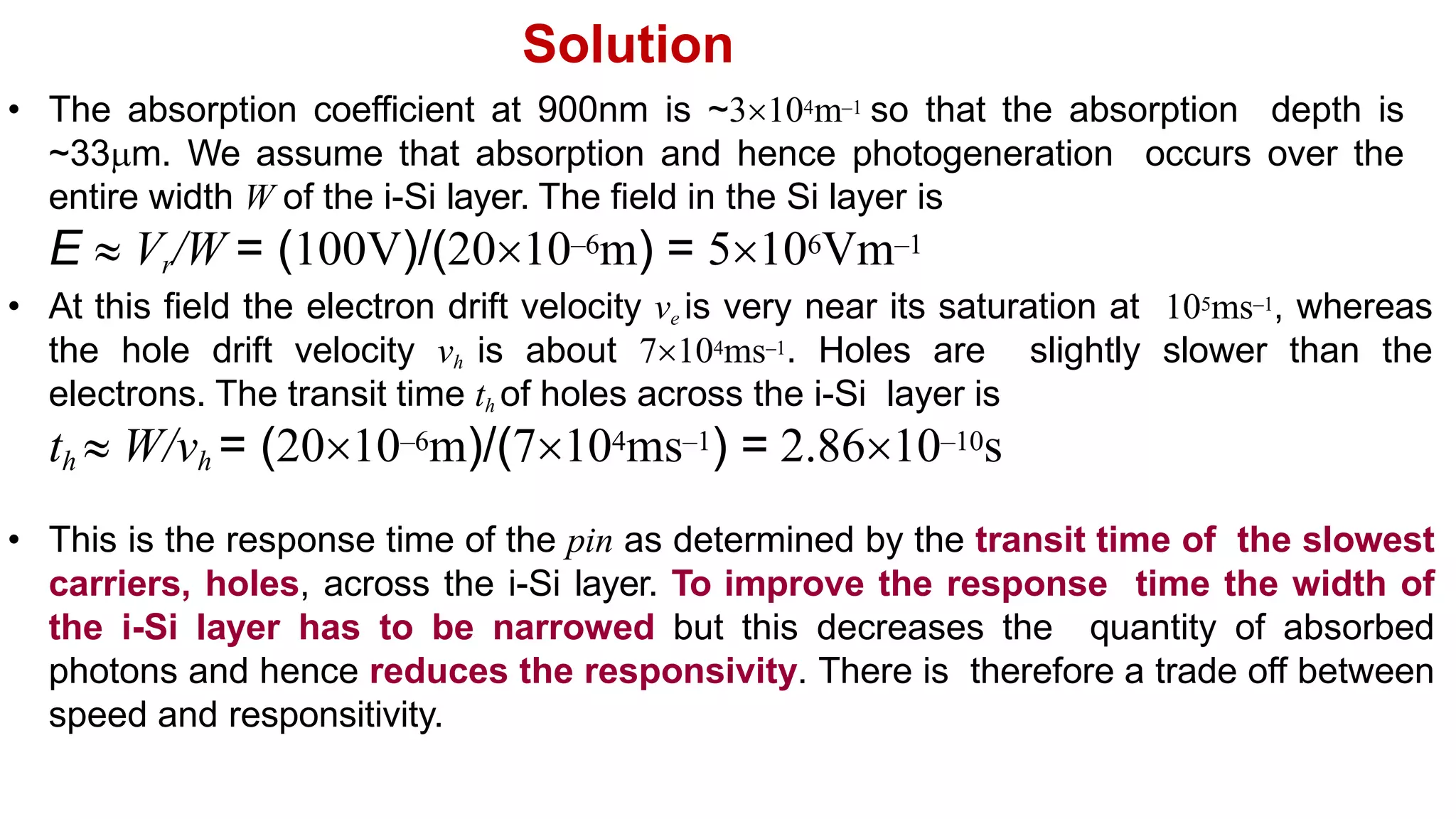
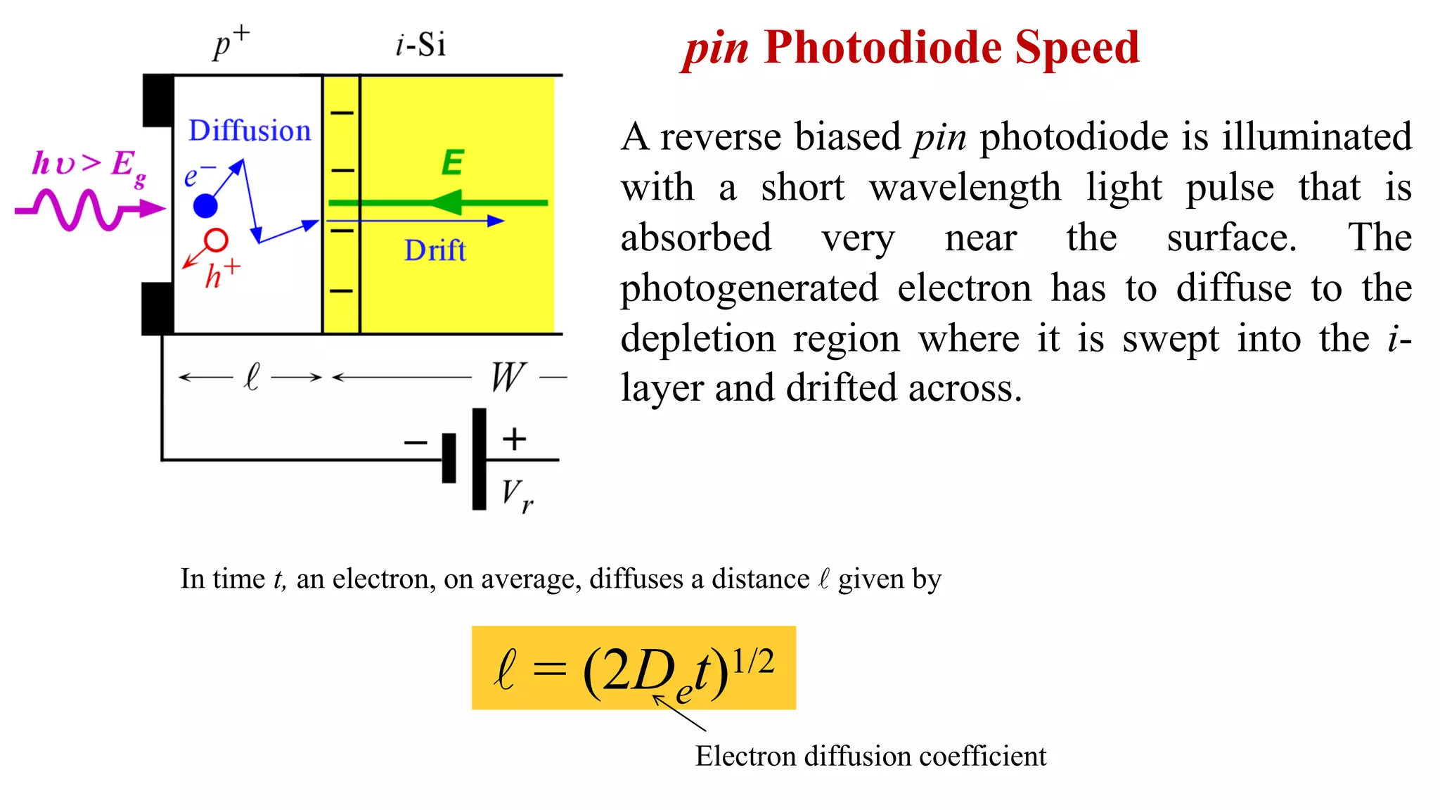
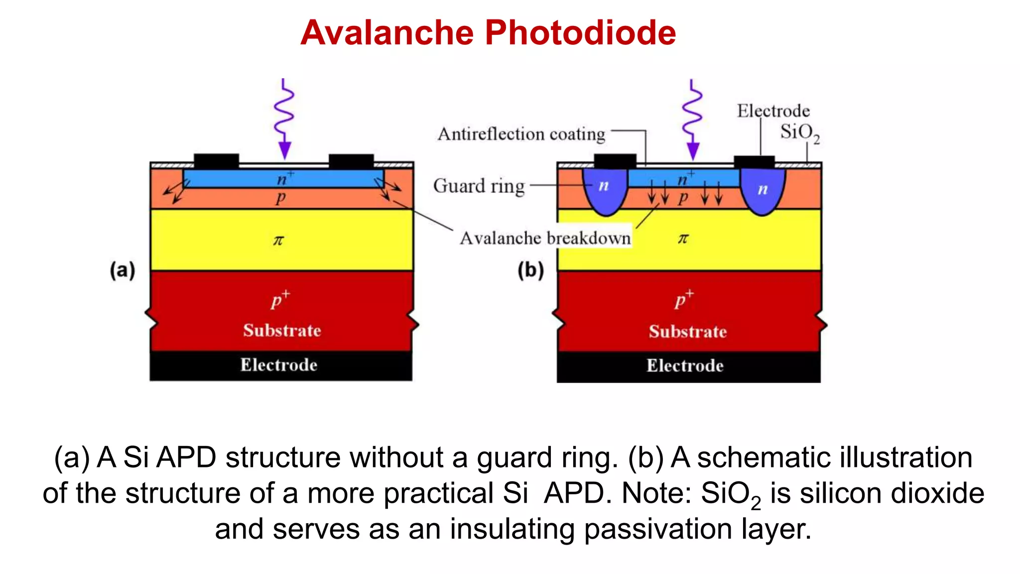
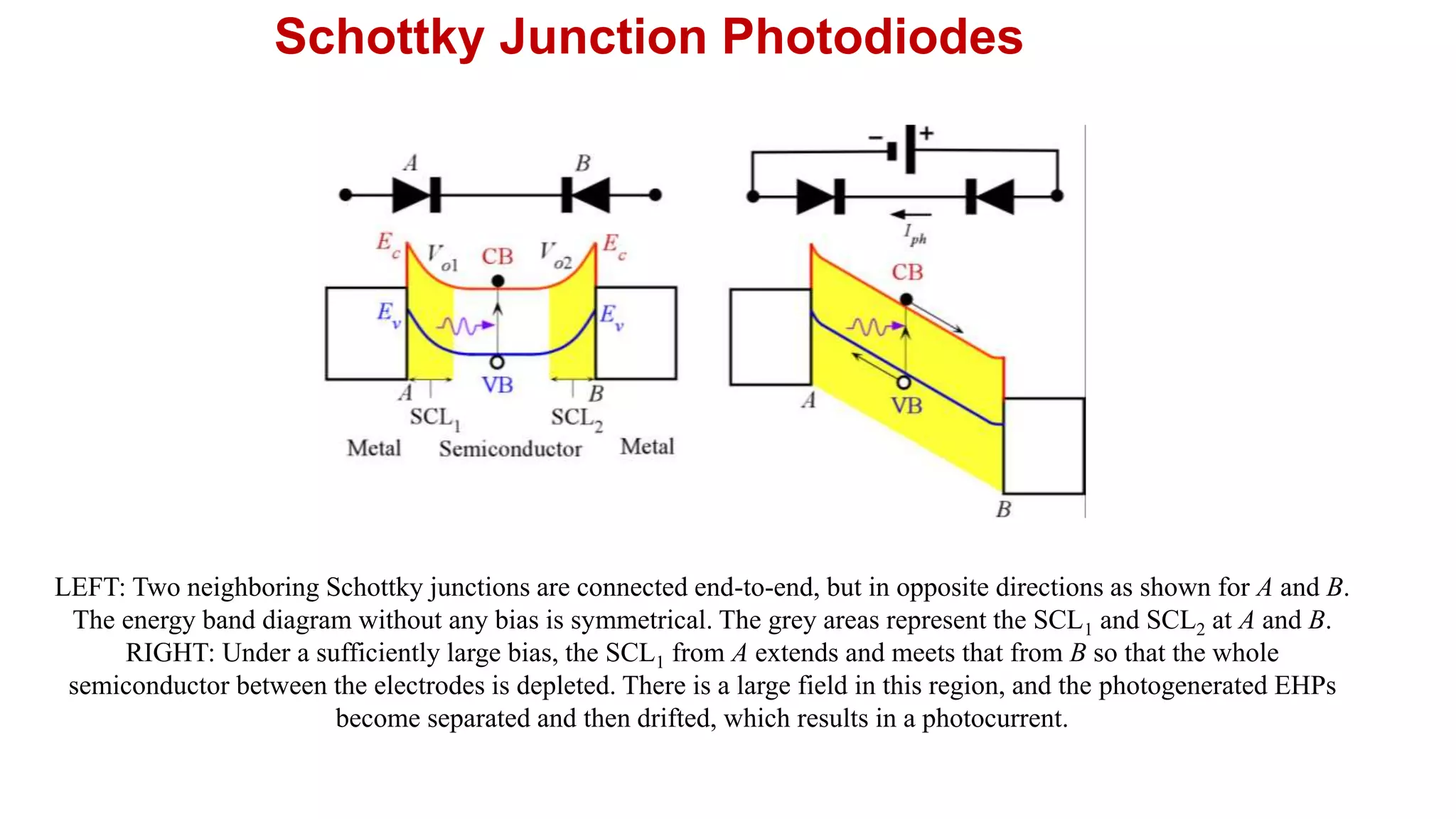
A pin photodiode operates as follows:
1. Photons are absorbed over the intrinsic (i-Si) layer, generating electron-hole pairs.
2. The built-in electric field separates and drifts the photogenerated carriers toward the contacts.
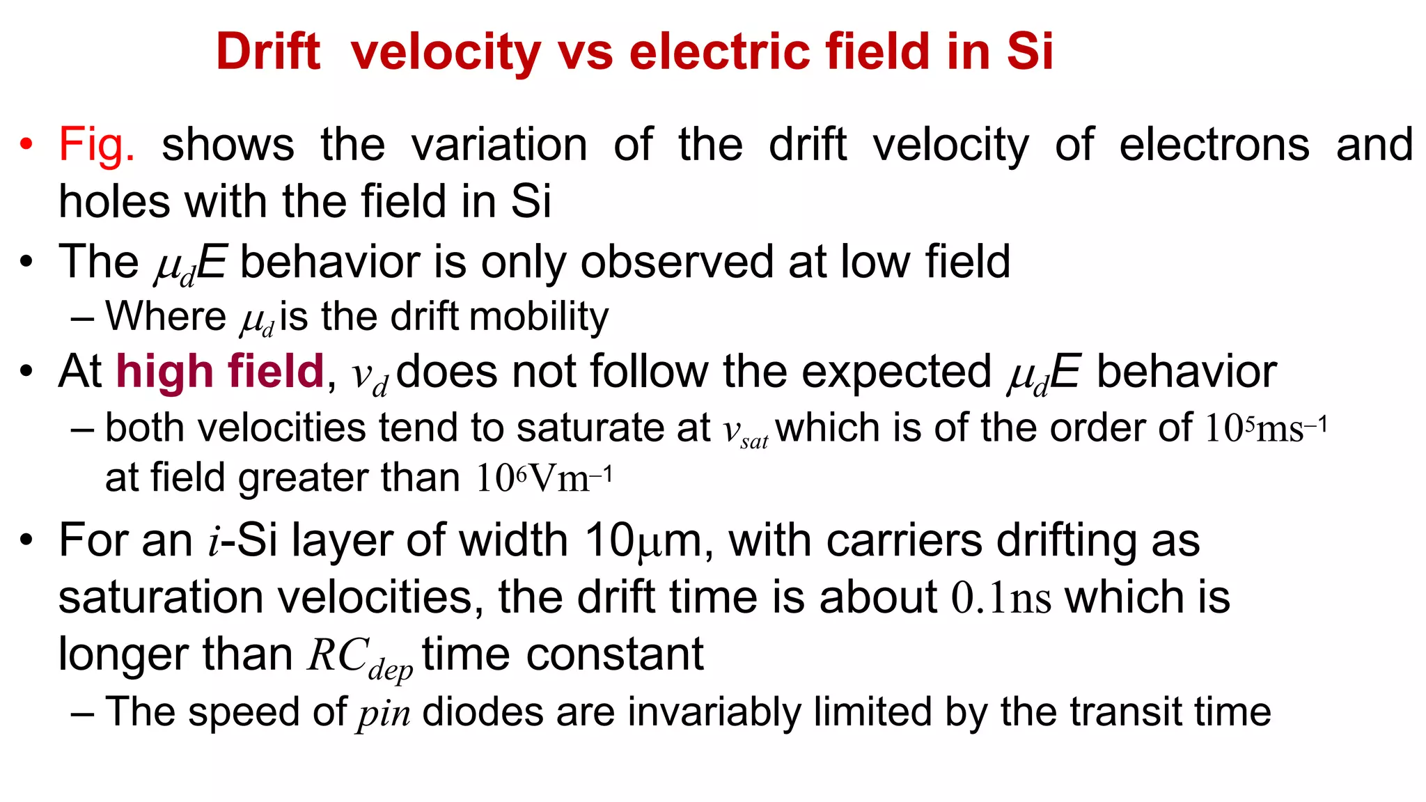
3. The transit time of carriers across the i-Si layer determines the response time of the pin photodiode. Wider i-Si layers absorb more photons but increase transit time.
![Internal Quantum Efficiency i
photons
absorbed
of
Number
ated
photogener
EHP
of
Number
y
Efficienc
Quantum
Internal
i
Assuming lp is very thin, and assuming W
>> Lh
)]
exp(
1
[
)
0
(
W
h
P
e
I o
i
ph a
u
T
T = Transmission coefficient of AR coating
a = Absorption coefficient](https://image.slidesharecdn.com/photodiodeandphotodetectors-230206141846-d5ac85f8/75/Photodiode-and-Photodetectors-pptx-11-2048.jpg)
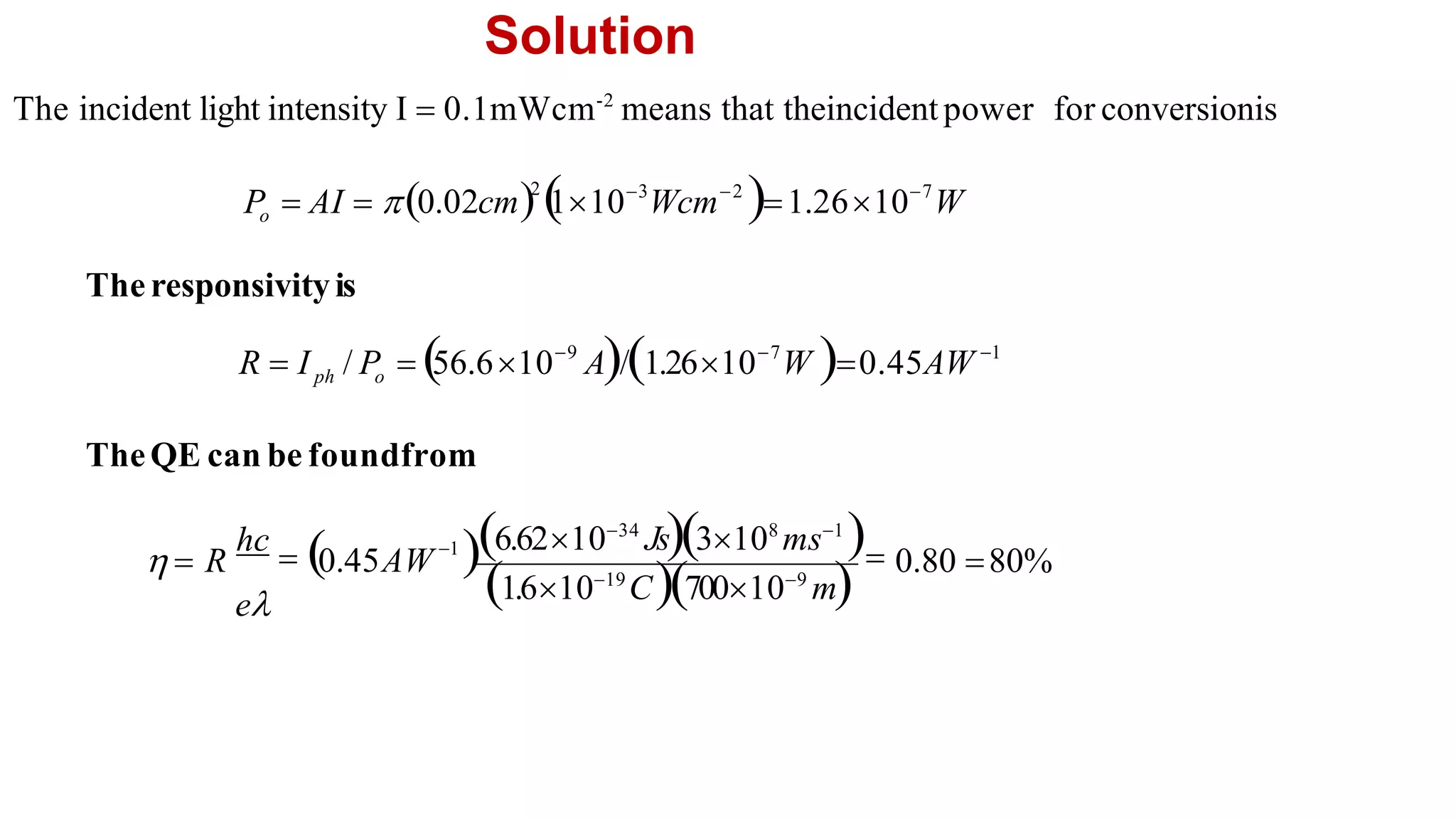

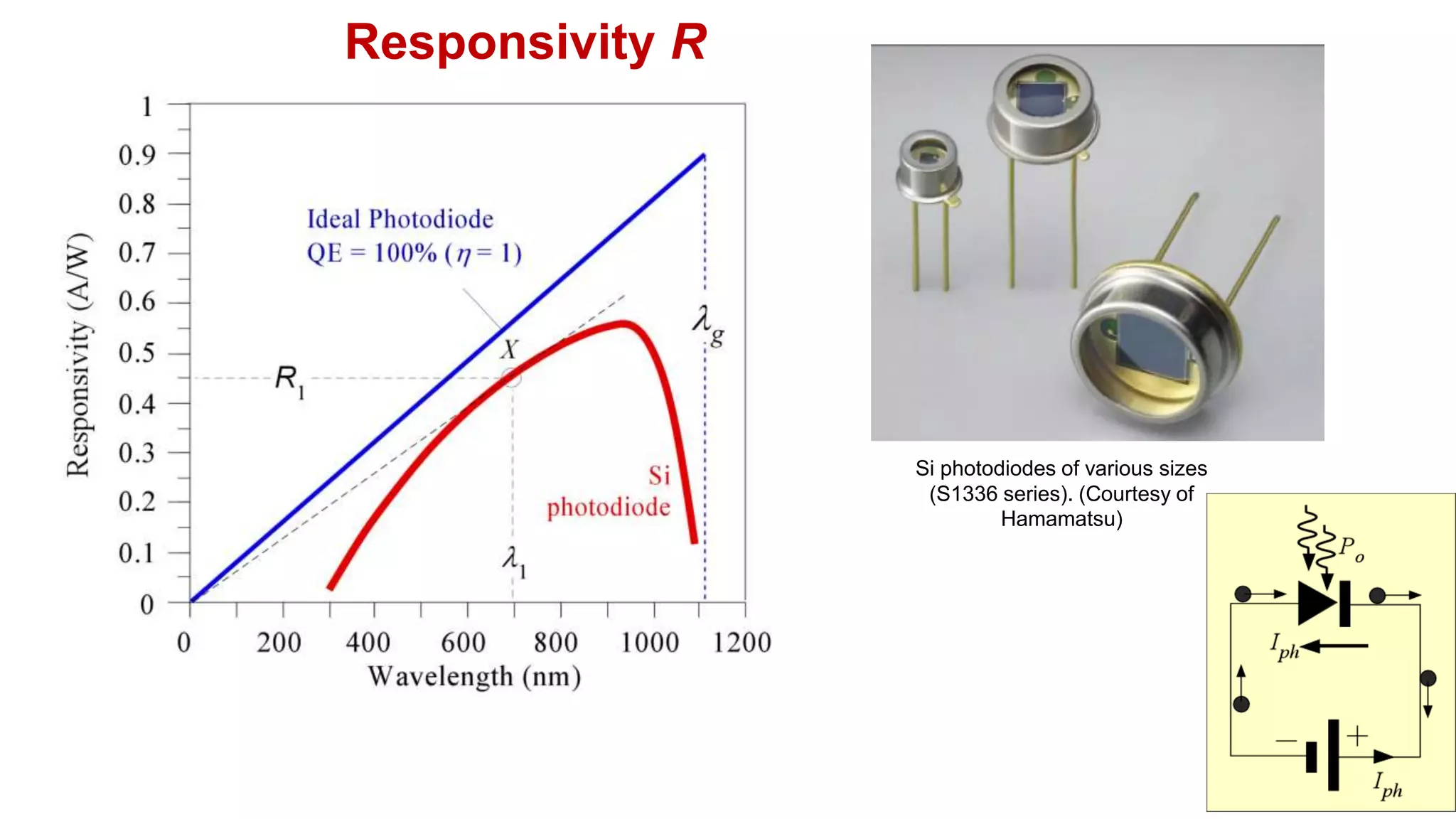
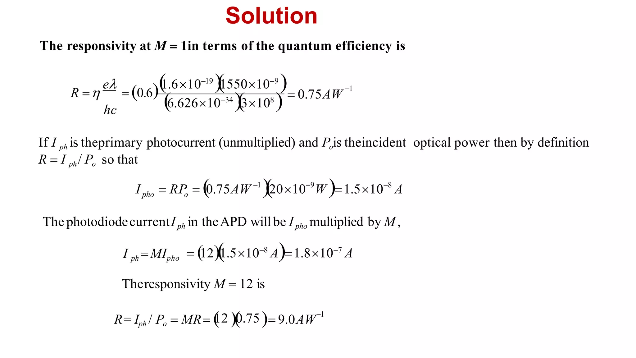
 = 1.2610-7 W or 0.126 W.
The responsivity is
R = Iph /Po = (56.6 10-9 A)/(1.2610-7 W ) = 0.45 A W-1
The QE can be found from
%
80
80
.
0
m)
10
C)(700
10
(1.6
)
s
m
10
s)(3
J
10
(6.62
)
W
A
45
.
0
( 9
19
-1
8
-34
1
-
e
hc
R](https://image.slidesharecdn.com/photodiodeandphotodetectors-230206141846-d5ac85f8/75/Photodiode-and-Photodetectors-pptx-33-2048.jpg)

![EXAMPLE : Photocarrier Diffusion in a pin photodiode
A reverse biased pin photodiode is illuminated with a short wavelength light pulse that is absorbed very
near the surface. The photogenerated electron has to diffuse to the depletion region where it is swept
into the i-layer and drifted across by the field in this region. What is the speed of response of this
photodiode if the i-Si layer is 20 m and the p+-layer is 1 m and the applied voltage is 60 V? The
diffusion coefficient (De) of electrons in the heavily doped p+-region is approximately 310-4 m2 s-1.
Solution
There is no electric field in the p+-side outside
the depletion region as shown in Figure 5.12 .
The photogenerated electrons have to make it
across to the n+-side to give rise to a
photocurrent. In the p+-side, the electrons
move by diffusion. In time t, an electron, on
average, diffuses a distance l given by
l = [2Det]1/2
The diffusion time tdiff is the time it takes for an
electron to diffuse across the p+-side (of length
l ) to reach the depletion layer and is given by](https://image.slidesharecdn.com/photodiodeandphotodetectors-230206141846-d5ac85f8/75/Photodiode-and-Photodetectors-pptx-36-2048.jpg)
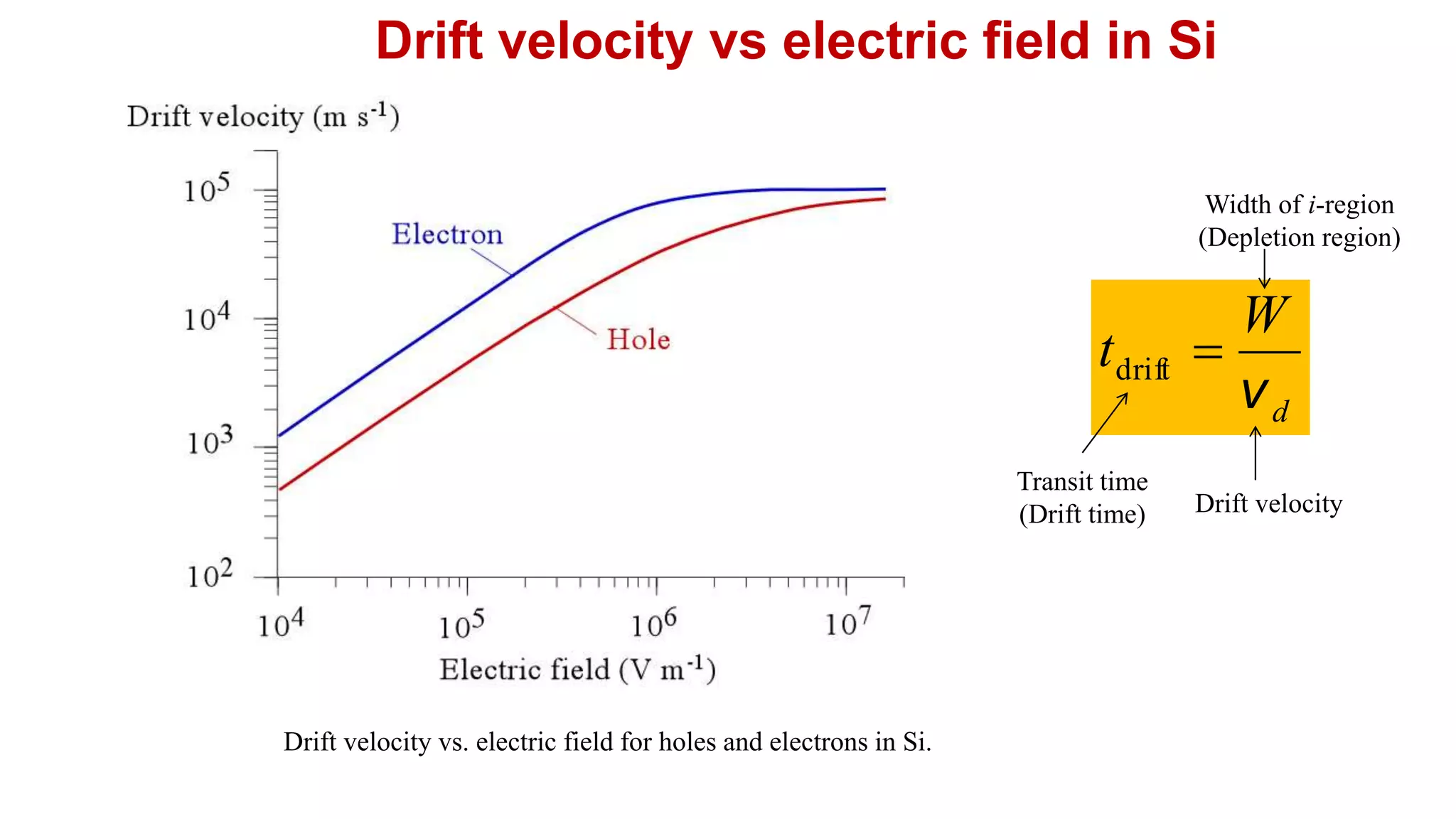
![EXAMPLE: Photocarrier Diffusion in a pin photodiode
Solution (continued)
tdiff = l 2/(2De) = (110-6 m)2 / [2(310-4 m2 s-1)] = 1.6710-9 s or 1.67 ns.
On the other hand, once the electron reaches the depletion region, it
becomes drifted across the width W of the i-Si layer at the saturation drift
velocity since the electric field here is E = Vr / W = 60 V / 20 m = 3106 V m-
1; and at this field the electron drift velocity ve saturates at 105 m s-1. The drift
time across the i-Si layer is
tdrift = W / ve = (2010-6 m) / (1105 m s-1) = 2.010-10 s or 0.2 ns.
Thus, the response time of the pin to a pulse of short wavelength
radiation that is absorbed near the surface is very roughly tdiff + tdrift or 1.87
ns. Notice that the diffusion of the electron is much slower than its drift. In a
proper analysis, we have to consider the diffusion and drift of many carriers,
and we have to average (tdiff + tdrift) for all the electrons.](https://image.slidesharecdn.com/photodiodeandphotodetectors-230206141846-d5ac85f8/75/Photodiode-and-Photodetectors-pptx-37-2048.jpg)
![EXAMPLE: Steady state photocurrent in the pin photodiode
We assume these will drift through the depletion region and thereby contribute to the
photocurrent. The current contribution d Iph from absorption and photogeneration at x
within the SCL will thus be
We can integrate this from x = 0 (assuming lp is very thin) to the end of x = W, and
assuming W >> Lh to find
Steady state photocurrent pin photodiode (5.5.4)
where the approximate sign embeds the many assumptions we made in deriving Eq. (5.5.4).
Consider a pin photodiode without an AR coating so that T = 0.68. Assume i = 1. The SCL
width is 20 m. If the device is to be used at 900 nm, what would be the photocurrent if the
incident radiation power is 100 nW? What is the responsivity? Find the photocurrent and
the responsivity if a perfect AR coating is used. What is the primary limiting factor? What is
the responsivity if W = 40 µm?
x
x
h
P
e
h
x
x
P
e
δI o
i
o
i
ph d
a
u
a
u
d
a
)
exp(
)
0
(
)
(
T
)]
exp(
1
[
)
0
(
W
h
P
e
I o
i
ph a
u
T](https://image.slidesharecdn.com/photodiodeandphotodetectors-230206141846-d5ac85f8/75/Photodiode-and-Photodetectors-pptx-39-2048.jpg)
![EXAMPLE: Steady state photocurrent in the pin photodiode
Solution (continued)
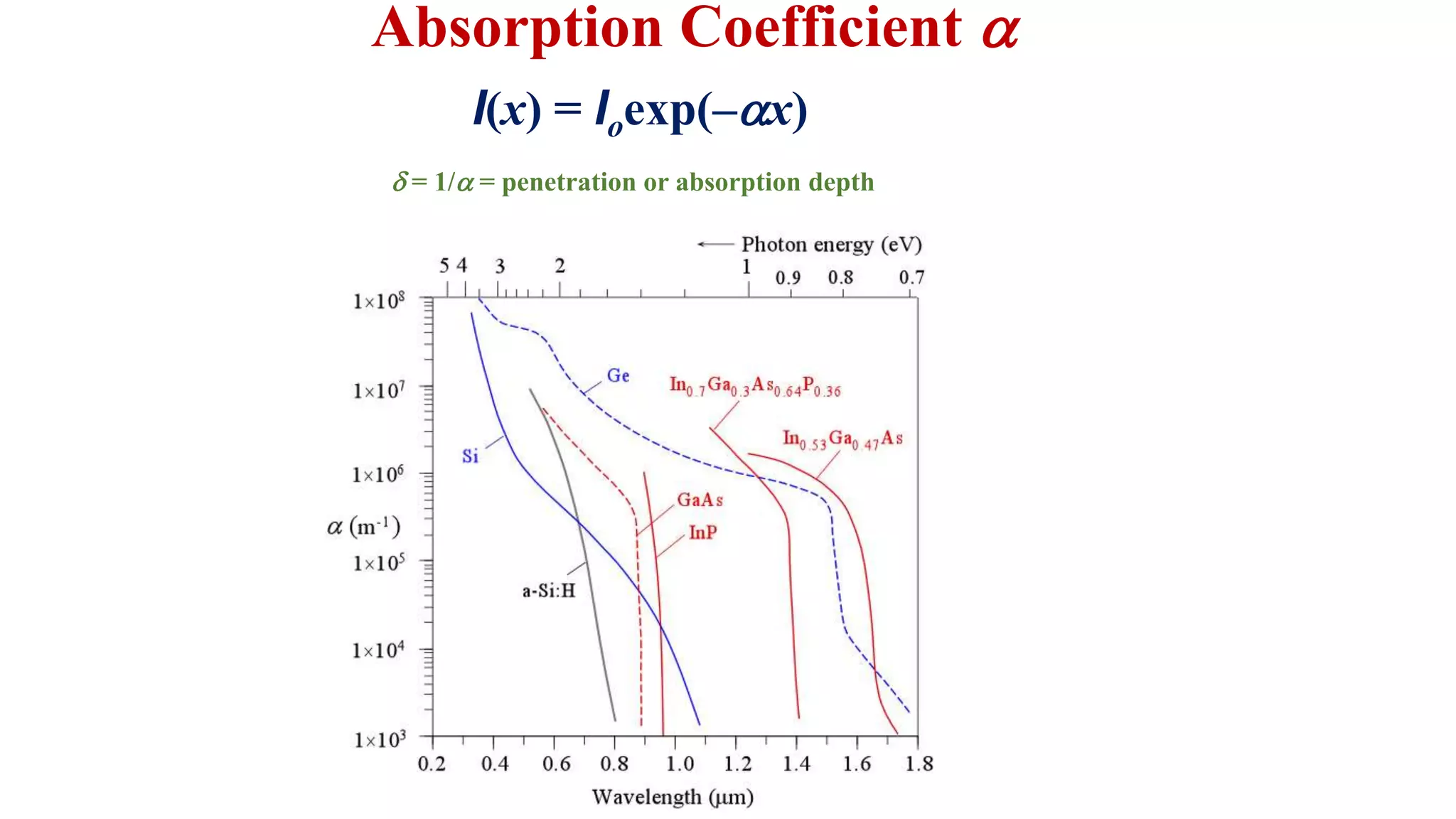
From Figure 5.5, at = 900 nm, a 3 ×10⁴ m-1. Further for =0.90 m, the photon
energy hu = 1.24 / 0.90 = 1.38 eV. Given Po(0) = 100 nW, we have
= 22 nA
and the responsivity R = 22 nA / 100 nW = 0.22 A W-1, which is on the low-side.
Consider next, a perfect AR coating so that T = 1, and using Eq. (5.5.4) again, we find
Iph = 32.7 nA and R = 0.33 A W-1, a significant improvement.
The factor [1exp(aW)] is only 0.451, and can be significantly improved by making
the SCL thicker. Setting W = 40 m, gives [1exp(aW)] = 0.70 and R = 0.51, which is
close to values for commercial devices.
The maximum theoretical photocurrent would be obtained by setting exp(aW) 0, T
= 1, i = 1, which gives Iph = 73 nA and R = 0.73 A W-1.
)]
10
20
10
3
exp(
1
[
)
10
6
.
1
38
.
1
(
)
10
100
)(
68
.
0
)(
1
)(
10
6
.
1
( 6
4
19
9
19
ph
I](https://image.slidesharecdn.com/photodiodeandphotodetectors-230206141846-d5ac85f8/75/Photodiode-and-Photodetectors-pptx-40-2048.jpg)
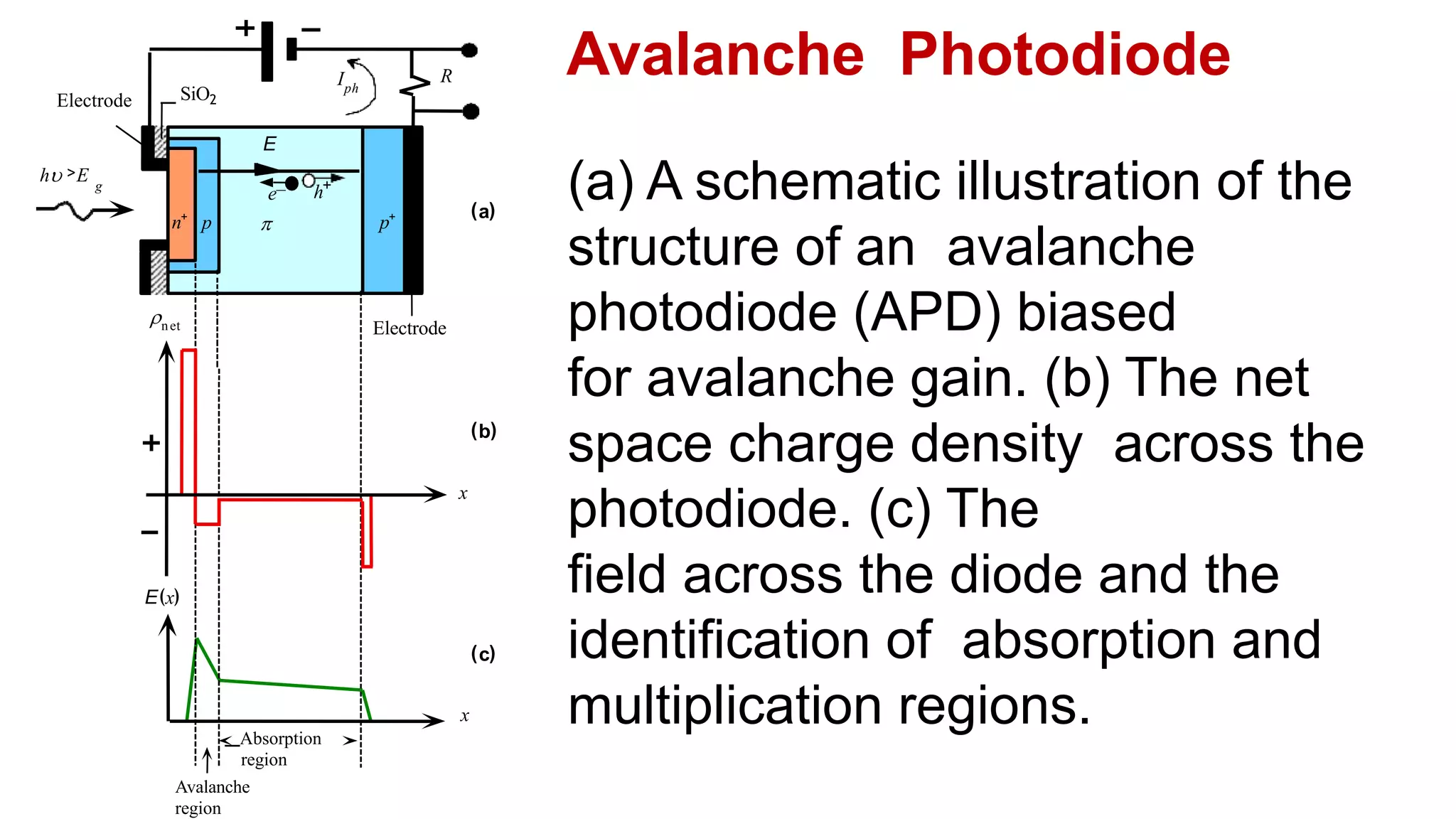

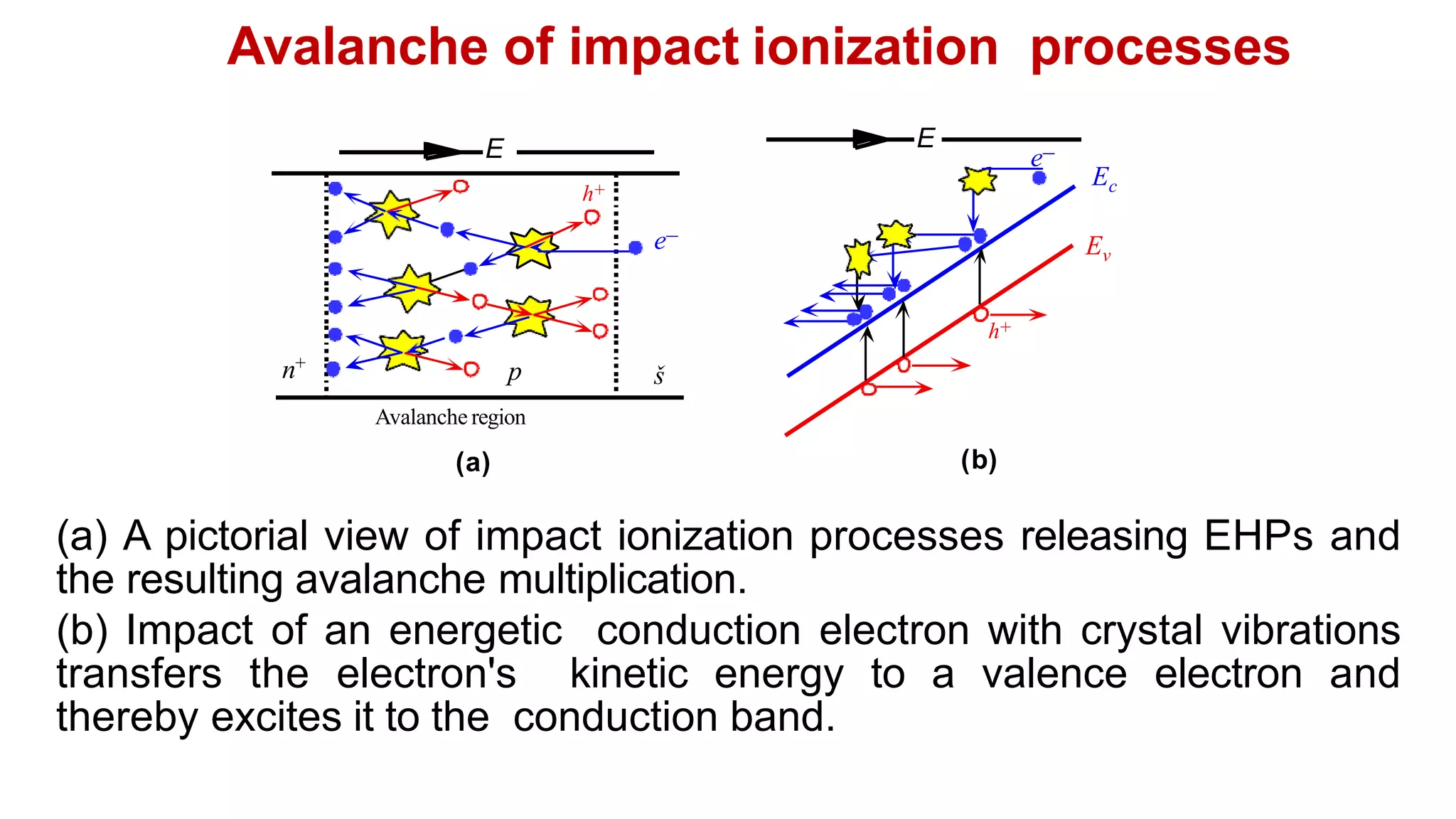

![Avalanche Photodiode Gain or Multiplication M
M = exp(aew)
Ionization coefficient
k
w
k
k
M
e
]
)
1
(
exp[
1
a
Electrons only
Electrons and holes
k ah / ae](https://image.slidesharecdn.com/photodiodeandphotodetectors-230206141846-d5ac85f8/75/Photodiode-and-Photodetectors-pptx-53-2048.jpg)


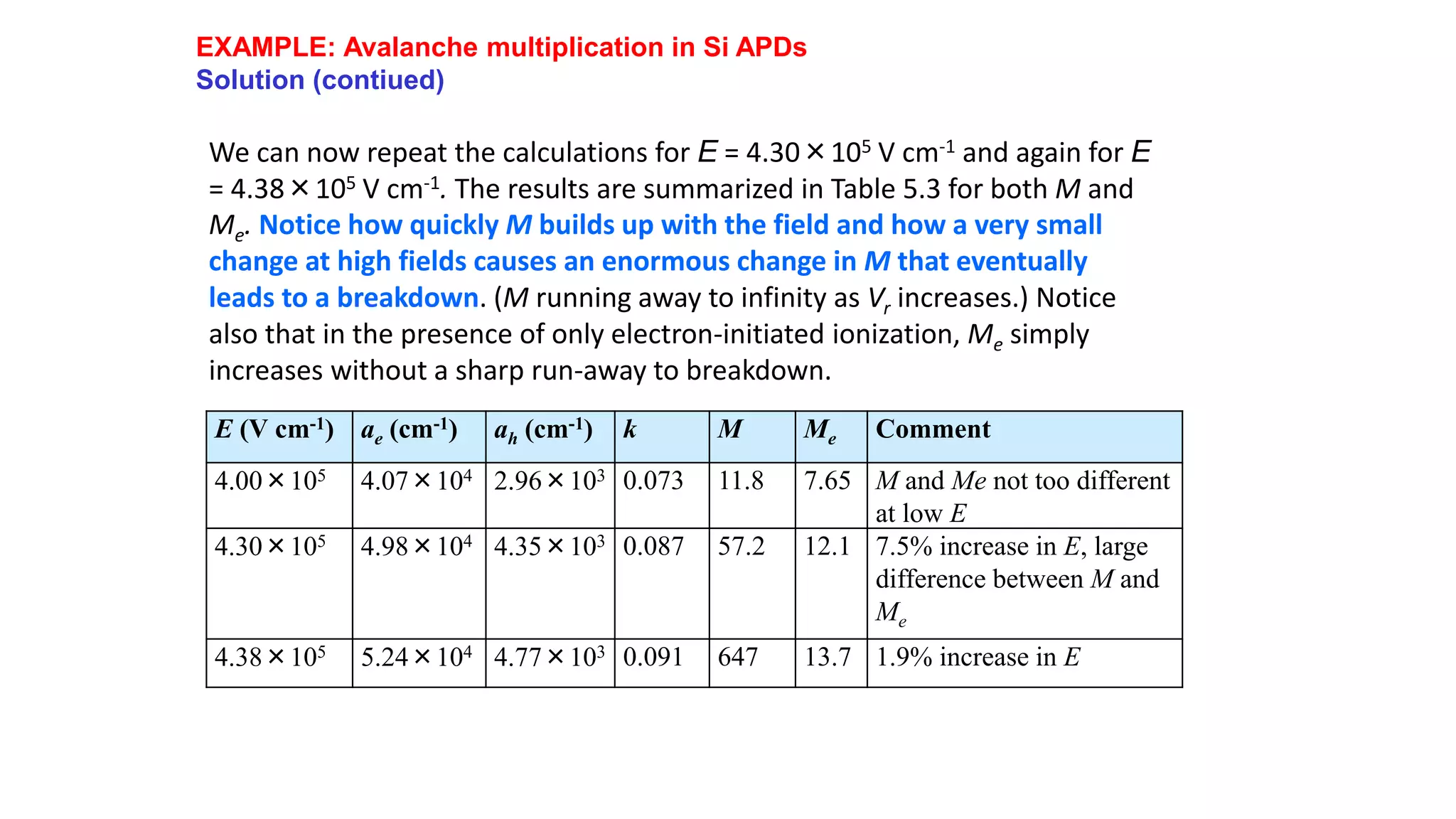
![EXAMPLE: Avalanche multiplication in Si APDs
The electron and hole ionization coefficients ae and ah in silicon are approximately given by Eq. (5.6.4)
with A 0.740×106 cm-1, B 1.16×10⁶ V cm-1 for electrons (ae) and A 0.725×106 cm-1 and B
2.2×10⁶ V cm-1 for holes (ah). Suppose that the width w of the avalanche region is 0.5 m. Find the
multiplication gain M when the applied field in this region reaches 4.00×10⁵ V cm-1, 4.30×10⁵ V cm-1
and 4.38×10⁵ V cm-1
. What is your conclusion?
Solution
At the field of E = 4.00×10⁵ V cm-1, from Eq. (5.6.4)
ae = Aexp(B/E)
= (0.74×106 cm-1)exp[1.16×10⁶ V cm-1)/(4.00×105 V cm-1)]
= 4.07×104 cm-1.
Similarly using Eq. (5.6.4) for holes, ah = 2.96×103 cm-1. Thus k = ah /ae = 0.073.
Using this k and ae above in Eq. (5.6.6) with w = 0.5×10⁻⁴ cm,
= 11.8
Note that if we had only electron avalanche without holes ionizing, then the
multiplication would be
Me = exp (aew) = exp[(4.07×104 cm-1)(0.5×10⁻⁴ cm)] = 7.65
073
.
0
)]
cm
10
5
.
0
)(
cm
10
07
.
4
)(
073
.
0
1
(
exp[
073
.
0
1
1
-
4
4
M](https://image.slidesharecdn.com/photodiodeandphotodetectors-230206141846-d5ac85f8/75/Photodiode-and-Photodetectors-pptx-68-2048.jpg)


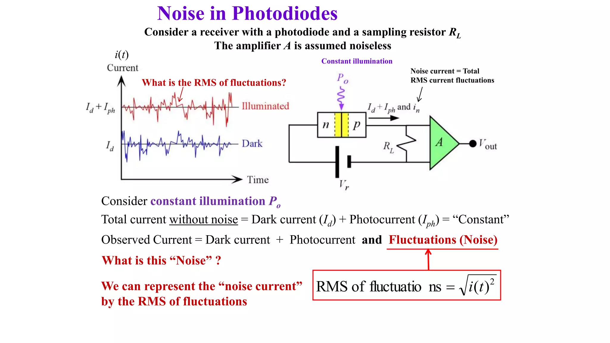
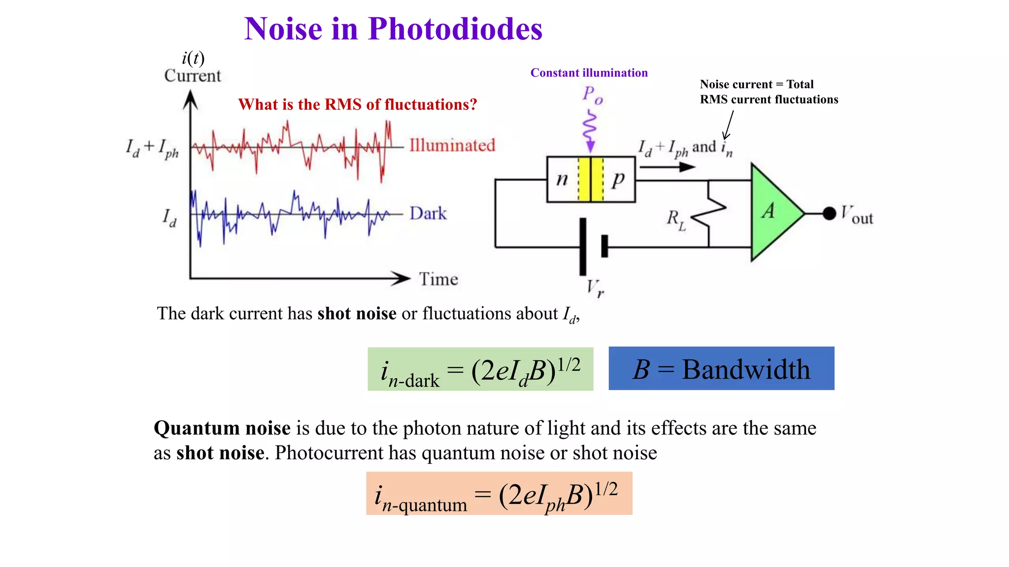
![Noise in Photodiodes
2
quantum
2
dark
2
n
n
n i
i
i
Total shot noise current, in
in = [2e(Id + Iph)B]1/2
We can conceptually view the photodetector current as
Id + Iph + in
This flows through a load resistor RL and voltage across RL is amplified by A to
give Vout
The noise voltage (RMS) due to shot noise in PD = inRLA](https://image.slidesharecdn.com/photodiodeandphotodetectors-230206141846-d5ac85f8/75/Photodiode-and-Photodetectors-pptx-103-2048.jpg)

![Summary of Noise in PD and RL
Important Note: Total noise is always found by first summing the average powers involved
in individual fluctuations e.g. power in shot noise + power in thermal noise
Power in shot noise in PD = in
2RL = [2e(Id + Iph)B]RL
Power in thermal fluctuations in RL = 4kBTB
Noise in the amplifier A must also be included
See advanced textbooks](https://image.slidesharecdn.com/photodiodeandphotodetectors-230206141846-d5ac85f8/75/Photodiode-and-Photodetectors-pptx-106-2048.jpg)

![Noise in Avalanche Photodiode (APD)
in-APD = Min = M[2e(Ido + Ipho)B]1/2
in-APD = [2e(Ido + Ipho)M2B]1/2
Ideally the shot noise is simply multiplied so that we
should expect
But, we observe excess noise above this shot noise
Avalanche Noise
in-APD = [2e(Ido + Ipho)M2FB]1/2
Excess Noise Factor](https://image.slidesharecdn.com/photodiodeandphotodetectors-230206141846-d5ac85f8/75/Photodiode-and-Photodetectors-pptx-112-2048.jpg)
![Noise in Avalanche Photodiode (APD)
Excess Avalanche Noise Factor F
in-APD = [2e(Ido + Ipho)M2FB]1/2
Excess Noise Factor
APDs exhibit excess avalanche noise due to the randomness of the impact
ionization process in the multiplication region. Some carriers travel far
and some short distances within this zone before they cause impact
ionization
F Mx where x is an index that depends on the
semiconductor, the APD structure and the type of carrier
that initiates the avalanche (electron or hole)
For Si APDs, x is 0.30.5 whereas for Ge and III-V (such as InGaAs)
alloys it is 0.71](https://image.slidesharecdn.com/photodiodeandphotodetectors-230206141846-d5ac85f8/75/Photodiode-and-Photodetectors-pptx-113-2048.jpg)
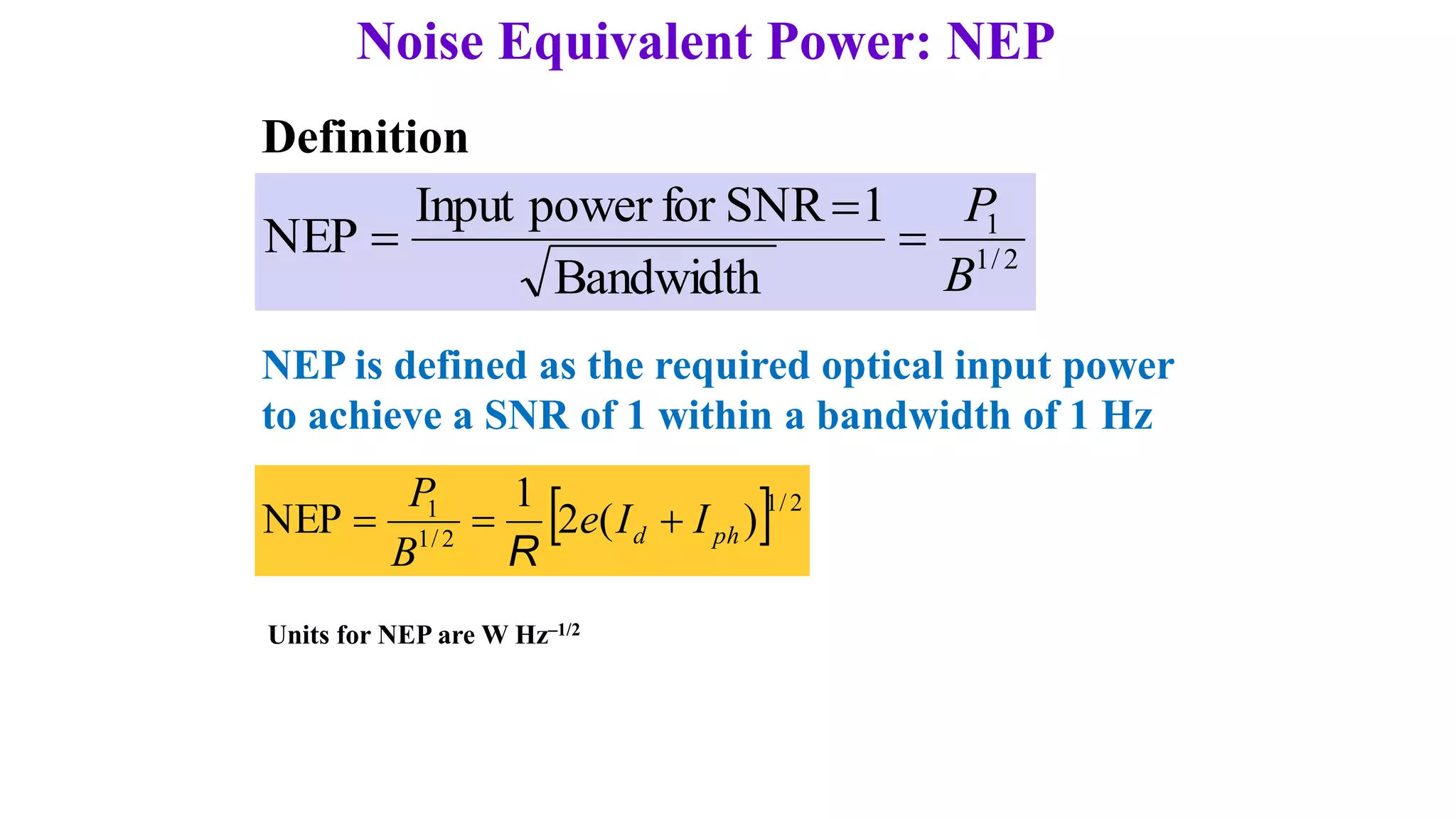
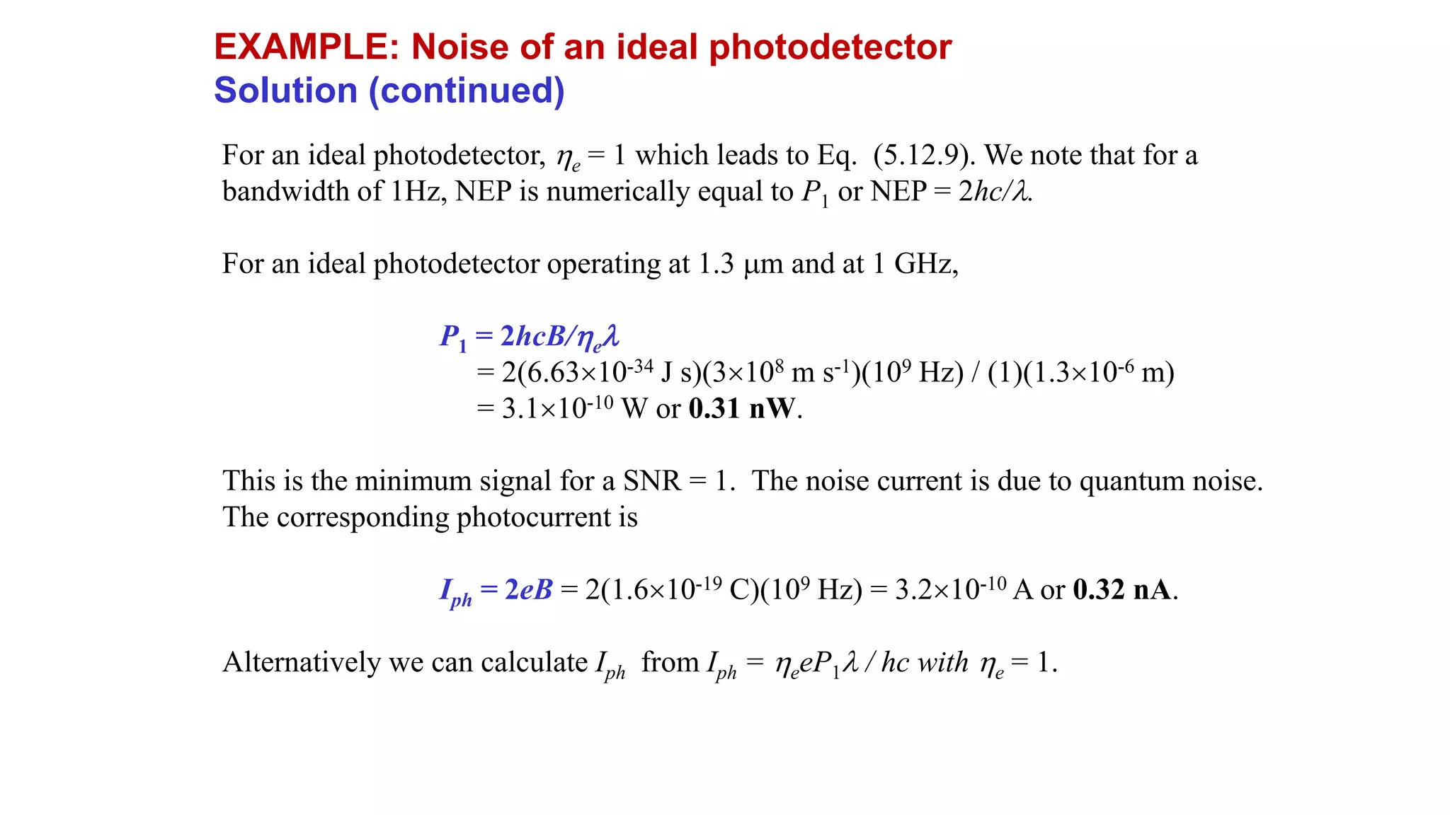
![EXAMPLE: Noise of an ideal photodetector
Consider an ideal photodiode with e = 1 (QE = 100%) and no dark current, Id = 0. Show that the
minimum optical power required for a signal to noise ratio (SNR) of 1 is
(5.12.9)
Calculate the minimum optical power for a SNR = 1 for an ideal photodetector operating at 1300 nm
with a bandwidth of 1 GHz? What is the corresponding photocurrent?
Solution
We need the incident optical power P1 that makes the photocurrent Iph equal to the
noise current in, so that SNR = 1. The photocurrent (signal) is equal to the noise
current when
Iph = in =[2e(Id + Iph)B]1/2 = [2eIphB]1/2
since Id = 0. Solving the above, Iph = 2eB
From Eqs. (5.4.3) and (5.4.4), the photocurrent Iph and the incident optical
power P1 are related by
Thus,
B
hc
P
2
1
eB
hc
eP
I e
ph 2
1
B
hc
P
e
2
1 ](https://image.slidesharecdn.com/photodiodeandphotodetectors-230206141846-d5ac85f8/75/Photodiode-and-Photodetectors-pptx-114-2048.jpg)


![EXAMPLE: SNR of a receiver
Solution (continued)
Shot noise current from the detector = [2e(Id + Iph)B]1/2 = 0.047 nA
= 1.29 nA
Thus, the noise contribution from RL is greater than that from the photodiode.
The SNR is
= 15.0
Generally SNR is quoted in decibels. We need 10log(SNR), or 10log(15.0)
i.e., 11.8 dB. Clearly, the load resistance has a dramatic effect on the overall noise
performance.
2
9
2
9
2
9
)
A
10
29
.
1
(
)
A
10
047
.
0
(
)
A
10
5
(
SNR
](https://image.slidesharecdn.com/photodiodeandphotodetectors-230206141846-d5ac85f8/75/Photodiode-and-Photodetectors-pptx-118-2048.jpg)
![EXAMPLE: Noise in an APD
Consider an InGaAs APD with x 0.7 which is biased to operate at M = 10. The unmultiplied dark current
is 10 nA and bandwidth is 700 MHz.
(a) What is the APD noise current per square root of bandwidth?
(b) What is the APD noise current for a bandwidth of 700 MHz?
(c) If the responsivity (at M = 1) is 0.8 A W-1 what is the minimum optical power for a SNR of 10?
Solution
(a) In the absence of any photocurrent, the noise in the APD comes from the
dark current. If the unmultipled dark current is Ido then the noise current (rms) is
in-dark = [2eIdoM2+xB]1/2
Thus,
= 1.27 10-12 A Hz-1/2 or 1.27 pA Hz-1/2.
(b) In a bandwidth B of 700 MHz, the noise current is
in-dark = (700106 Hz)1/2(1.27 pA Hz-1/2)
= 3.3510-8 A or 33.5 nA.
7
.
0
2
9
19
2
dark
)
10
)(
A
10
10
)(
C
10
6
.
1
(
2
2
B
x
do
n
M
eI
i](https://image.slidesharecdn.com/photodiodeandphotodetectors-230206141846-d5ac85f8/75/Photodiode-and-Photodetectors-pptx-119-2048.jpg)
![EXAMPLE: Noise in an APD
Solution (continued)
(c) The SNR with a primary photocurrent Ipho in the APD is
Rearranging to obtain Ipho we get,
This is a quadratic equation in Ipho with defined coefficients since M, x, B, Ido and
SNR are given. Solving this quadratic with a SNR = 10 for Ipho we find
Ipho 1.76 10-8 A or 17.6 nA
While it may seem odd that Ipho is less than the dark noise current (33.5 nA) itself,
the actual photocurrent Iph however is 176 nA, since it is multiplied by M. Further the
total noise current, in-APD = [2e(Ido + Ipho)M2+xB]1/2 is 55.7 nA so that one can easily
check that SNR = Iph
2 / i2
n-APD is indeed 10.
By the definition of responsivity, R = Ipho/Po, we find,
Po = Ipho / R = (1.7610-8 A)/(0.8 A W-1) = 2.210-8 W or 22 nW
2 2
2
Signal Power
SNR
Noise Power 2 ( )
pho
x
do pho
M I
e I I M B
0
]
)
SNR
(
2
[
)]
SNR
(
2
[
)
( 2
2
2
2
do
x
pho
x
pho I
B
eM
I
B
eM
I
M](https://image.slidesharecdn.com/photodiodeandphotodetectors-230206141846-d5ac85f8/75/Photodiode-and-Photodetectors-pptx-120-2048.jpg)