SlideShare a Scribd company logo
1 of 14
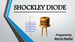
SHOCKLEY DIODE
Prepared by
Barira Nashal
Contents
Introduction
Construction
Working or characteristics
Application
Introduction
The term Shockley diode or PNPN diode is named from the
inventor “William Shockley”.
It is a four layer semiconductor device and it was the first
semiconductor devices.
It is similar to a thyristor with detached gate.
This type of diode is not available commercially and not
particularly useful. But, this diode is more useful in making other
kinds of thyristors such as DIAC,TRIAC and SCR.
Internal Structure And Symbol
EquivalentCircuitDiagram
Construction
The construction of this diode is done by connecting the four
layers to form PNPN junction.The basic circuit of this diode using
two transistors. In the circuit, the collector terminal of the
T1 transistor is connected to the base terminal of theT2
transistor.
The J1 junction is designed at the EB junction ofT1 transistor,
J2 is at common connected BC junction betweenT1 &T2
transistors,
J3 is at BE junction ofT2 transistor.
So, as the BE junctions, J1& J3 must be forward biased & as a CB
junction, J2 must be reverse biased for linear operation.
Working
The shockley diode functions like a normal thyristor without any
trigger inputs . When the diode is in the forward, the current
flows through the diode, whereas in reverse bias, there is no flow
of current.
The Shockley diode comprises of three junctions namely J1, J2
and J3. Whenever the voltage is applied to the diode then the
anode terminal is made positive with respect to the cathode, J1
and J3 junctions are forward biased where J2 is reverse biased.
Forward Biasing
When the voltage is applied to the shockley diode in such a
way that anode is made positive with respect to cathode,
junctions J1 and J3 are forward biased and J2 is reverse biased.
Until the voltage across the diode is less than the break over
voltage, as an open switch shockley diode exhibits a very high
resistance and allows no current to flow through it.
Once the break over voltage is reached (as the forward
voltage is increased), it exhibits a very low resistance due to
the breakdown of junction J2.
Therefore, it acts like a short circuit and allows the current to
flow until the current reaches to the holding current level of
the diode.
ON-state current flows only when the voltage is more than
the break over voltageVBO.
Reverse Biasing
When the anode is made negative with respect to
the cathode, junctions J1 and J3 are reverse biased
and junction J2 is forward biased.
If the reverse bias voltage is increased (beyond
the breakdown voltage of the shockley diode), J1
and J3 are reverse biased, then the reverse current
will flow through the diode.
This reverse current produces the heat, further
this could ruin the entire diode.
Therefore, shockley diode should never be
operated in reverse biased condition with a
voltage equal to the reverse breakdown voltage.
To Turn Off Diode ..
Once the shockley diode is ON it acts like a closed switch offer a
very low resistance to the current flow.To turn OFF the diode,
the applied voltage must be reduced to a value such that current
flowing through the diode is less than the holding current IH of
the diode. In this state, junction J2 comes from reverse
breakdown state and restores its high resistance value.
Characteristics curve
Applications
1. Shockley Diode used as Relaxation
Oscillator:
When the battery voltage is applied to the circuit, the
capacitor charges through a resistance R.
When the applied voltage or voltage across the capacitor is
more than the break over voltage of shockley diode, it
becomes turned ON and acts as a Switch.
This causes rapidly to discharge the capacitor through the
diode.
When the current through the diode is less than the holding
current of the diode, the diode becomes turned OFF and
capacitor charges again.
The voltage across the capacitor isVBO where the voltage at
the reference is more than zero volts because the capacitor
will not discharge completely.
2. Shockley Diode used asTrigger Switch:
Most common applications of shockley diode are
switching circuits , to turn ON the SCR. SCR is triggered
by the shockley diode.The Resistive and capacitor RC
network is fed with a DC supply which drives the
shockley diode.
When theVDC is applied, shockley is forward biased and
also capacitor starts charging through the resistance.
When the charging voltage of the capacitor reaches to
the break over voltage of the diode, diode starts
conducting and the capacitor starts discharging through
the diode.This conduction of shockley diode drives the
SCR into turn ON state, then the buzzer gives an alarm.
Once the SCR is turned ON it will remain in the latching
or ON state until the power is removed.The triggering
times of SCR is controlled by selecting proper values of
capacitor and resistors.
Thank You !!!

More Related Content

What's hot

Thyristors (2)
Thyristors (2)Thyristors (2)
Thyristors (2)Chethan Sp
 
Bio-polar junction transistor (edc)
Bio-polar junction transistor  (edc)Bio-polar junction transistor  (edc)
Bio-polar junction transistor (edc)Abhinay Potlabathini
 
Unijunction transistor (ujt)
Unijunction transistor (ujt)Unijunction transistor (ujt)
Unijunction transistor (ujt)Sushama Nikam
 
EST 130, Transistor Biasing and Amplification.
EST 130, Transistor Biasing and Amplification.EST 130, Transistor Biasing and Amplification.
EST 130, Transistor Biasing and Amplification.CKSunith1
 
Unijunction transistor
Unijunction transistorUnijunction transistor
Unijunction transistorhepzijustin
 
Op amp(operational amplifier)
Op amp(operational amplifier)Op amp(operational amplifier)
Op amp(operational amplifier)Kausik das
 
Unit-I Characteristics of opamp
Unit-I Characteristics of opampUnit-I Characteristics of opamp
Unit-I Characteristics of opampDr.Raja R
 
Zener Diode-As Voltage Regulator
Zener Diode-As Voltage RegulatorZener Diode-As Voltage Regulator
Zener Diode-As Voltage RegulatorAdeel Rasheed
 
Operational amplifier
Operational amplifierOperational amplifier
Operational amplifiershire ali
 
Presentation on half and full wave ractifier.ppt
Presentation on half and full wave ractifier.pptPresentation on half and full wave ractifier.ppt
Presentation on half and full wave ractifier.pptKawsar Ahmed
 
Halfwave and full wave rectificaton
Halfwave and full wave rectificaton Halfwave and full wave rectificaton
Halfwave and full wave rectificaton University of Karachi
 
Basic of Diode Rectifiers
Basic of Diode RectifiersBasic of Diode Rectifiers
Basic of Diode Rectifiersssuser4b487e1
 
Clipper_and_clamper.ppt
Clipper_and_clamper.pptClipper_and_clamper.ppt
Clipper_and_clamper.pptAbhishekghjgj
 

What's hot (20)

Transistor configurations
Transistor configurationsTransistor configurations
Transistor configurations
 
Thyristors (2)
Thyristors (2)Thyristors (2)
Thyristors (2)
 
Bio-polar junction transistor (edc)
Bio-polar junction transistor  (edc)Bio-polar junction transistor  (edc)
Bio-polar junction transistor (edc)
 
Ujt uni junction transistor - basics
Ujt   uni junction transistor - basicsUjt   uni junction transistor - basics
Ujt uni junction transistor - basics
 
Semiconductor diode
Semiconductor diodeSemiconductor diode
Semiconductor diode
 
Unijunction transistor (ujt)
Unijunction transistor (ujt)Unijunction transistor (ujt)
Unijunction transistor (ujt)
 
EST 130, Transistor Biasing and Amplification.
EST 130, Transistor Biasing and Amplification.EST 130, Transistor Biasing and Amplification.
EST 130, Transistor Biasing and Amplification.
 
Clampers
ClampersClampers
Clampers
 
Unijunction transistor
Unijunction transistorUnijunction transistor
Unijunction transistor
 
Transistor biasing
Transistor biasing Transistor biasing
Transistor biasing
 
Hybrid Parameter in BJT
Hybrid Parameter in BJTHybrid Parameter in BJT
Hybrid Parameter in BJT
 
Op amp(operational amplifier)
Op amp(operational amplifier)Op amp(operational amplifier)
Op amp(operational amplifier)
 
Clipper and clampers
Clipper and clampersClipper and clampers
Clipper and clampers
 
Unit-I Characteristics of opamp
Unit-I Characteristics of opampUnit-I Characteristics of opamp
Unit-I Characteristics of opamp
 
Zener Diode-As Voltage Regulator
Zener Diode-As Voltage RegulatorZener Diode-As Voltage Regulator
Zener Diode-As Voltage Regulator
 
Operational amplifier
Operational amplifierOperational amplifier
Operational amplifier
 
Presentation on half and full wave ractifier.ppt
Presentation on half and full wave ractifier.pptPresentation on half and full wave ractifier.ppt
Presentation on half and full wave ractifier.ppt
 
Halfwave and full wave rectificaton
Halfwave and full wave rectificaton Halfwave and full wave rectificaton
Halfwave and full wave rectificaton
 
Basic of Diode Rectifiers
Basic of Diode RectifiersBasic of Diode Rectifiers
Basic of Diode Rectifiers
 
Clipper_and_clamper.ppt
Clipper_and_clamper.pptClipper_and_clamper.ppt
Clipper_and_clamper.ppt
 

Similar to Shockley Diode

lec 03 Power diode and types-1.pptx
lec 03 Power diode and types-1.pptxlec 03 Power diode and types-1.pptx
lec 03 Power diode and types-1.pptxZeeshanEjaz10
 
Types of Diodes
Types of DiodesTypes of Diodes
Types of DiodesMoin Aman
 
Basics and types_of_diodes
Basics and types_of_diodesBasics and types_of_diodes
Basics and types_of_diodesbadarhusnain
 
Electronic Devices - Special Diodes - Unit 1.pptx
Electronic Devices - Special Diodes - Unit 1.pptxElectronic Devices - Special Diodes - Unit 1.pptx
Electronic Devices - Special Diodes - Unit 1.pptxDhivya Ramachandran
 
Ch2-Diode.for electrical and computer engineering
Ch2-Diode.for electrical and computer engineeringCh2-Diode.for electrical and computer engineering
Ch2-Diode.for electrical and computer engineeringabdiihuseen31
 
PE4MSc_Ch1_SC_devices.pptx
PE4MSc_Ch1_SC_devices.pptxPE4MSc_Ch1_SC_devices.pptx
PE4MSc_Ch1_SC_devices.pptxAddisuMengesha2
 
Diode data sheet for alarm type project
Diode data sheet for alarm type projectDiode data sheet for alarm type project
Diode data sheet for alarm type projectmegha agrawal
 
Electrical and Electronics Engineering
Electrical and Electronics EngineeringElectrical and Electronics Engineering
Electrical and Electronics EngineeringEkeeda
 
Basic electronics (p-n Junction)
Basic electronics (p-n Junction)Basic electronics (p-n Junction)
Basic electronics (p-n Junction)Hitarth Patel
 
SCR NEW FOR TOMMOROW.pdf
SCR  NEW FOR TOMMOROW.pdfSCR  NEW FOR TOMMOROW.pdf
SCR NEW FOR TOMMOROW.pdfyogeshkute
 
Tanya makkar (5003)
Tanya makkar (5003)Tanya makkar (5003)
Tanya makkar (5003)Tanya Makkar
 

Similar to Shockley Diode (20)

lec 03 Power diode and types-1.pptx
lec 03 Power diode and types-1.pptxlec 03 Power diode and types-1.pptx
lec 03 Power diode and types-1.pptx
 
Diodes
DiodesDiodes
Diodes
 
Types of Diodes
Types of DiodesTypes of Diodes
Types of Diodes
 
Basics and types_of_diodes
Basics and types_of_diodesBasics and types_of_diodes
Basics and types_of_diodes
 
Electronic Devices - Special Diodes - Unit 1.pptx
Electronic Devices - Special Diodes - Unit 1.pptxElectronic Devices - Special Diodes - Unit 1.pptx
Electronic Devices - Special Diodes - Unit 1.pptx
 
Ch2-Diode.for electrical and computer engineering
Ch2-Diode.for electrical and computer engineeringCh2-Diode.for electrical and computer engineering
Ch2-Diode.for electrical and computer engineering
 
PE4MSc_Ch1_SC_devices.pptx
PE4MSc_Ch1_SC_devices.pptxPE4MSc_Ch1_SC_devices.pptx
PE4MSc_Ch1_SC_devices.pptx
 
Bsc 1 cbcs e1 unit 2
Bsc 1 cbcs e1 unit 2Bsc 1 cbcs e1 unit 2
Bsc 1 cbcs e1 unit 2
 
Diode data sheet for alarm type project
Diode data sheet for alarm type projectDiode data sheet for alarm type project
Diode data sheet for alarm type project
 
Diode
DiodeDiode
Diode
 
Chapter2
Chapter2Chapter2
Chapter2
 
power electronics
power electronicspower electronics
power electronics
 
SCR
SCRSCR
SCR
 
Electrical and Electronics Engineering
Electrical and Electronics EngineeringElectrical and Electronics Engineering
Electrical and Electronics Engineering
 
Basic electronics (p-n Junction)
Basic electronics (p-n Junction)Basic electronics (p-n Junction)
Basic electronics (p-n Junction)
 
Chapter 1.
Chapter 1.Chapter 1.
Chapter 1.
 
ELECTRONICS DEVICES AND CIRCUITS
ELECTRONICS DEVICES AND CIRCUITSELECTRONICS DEVICES AND CIRCUITS
ELECTRONICS DEVICES AND CIRCUITS
 
SCR NEW FOR TOMMOROW.pdf
SCR  NEW FOR TOMMOROW.pdfSCR  NEW FOR TOMMOROW.pdf
SCR NEW FOR TOMMOROW.pdf
 
8. semiconductors.rr
8. semiconductors.rr8. semiconductors.rr
8. semiconductors.rr
 
Tanya makkar (5003)
Tanya makkar (5003)Tanya makkar (5003)
Tanya makkar (5003)
 

More from Barira Khan

Ardu sat (Arduino based satellite)
Ardu sat (Arduino based satellite)Ardu sat (Arduino based satellite)
Ardu sat (Arduino based satellite)Barira Khan
 
Virtual Instrument
Virtual InstrumentVirtual Instrument
Virtual InstrumentBarira Khan
 
Iconoscope camera tube
Iconoscope camera tubeIconoscope camera tube
Iconoscope camera tubeBarira Khan
 
Frequency modulation and its circuits
Frequency modulation and its circuitsFrequency modulation and its circuits
Frequency modulation and its circuitsBarira Khan
 
Training of astronauts
Training of astronauts Training of astronauts
Training of astronauts Barira Khan
 
Computer summary
Computer summaryComputer summary
Computer summaryBarira Khan
 

More from Barira Khan (8)

Ardu sat (Arduino based satellite)
Ardu sat (Arduino based satellite)Ardu sat (Arduino based satellite)
Ardu sat (Arduino based satellite)
 
Virtual Instrument
Virtual InstrumentVirtual Instrument
Virtual Instrument
 
Management
ManagementManagement
Management
 
Iconoscope camera tube
Iconoscope camera tubeIconoscope camera tube
Iconoscope camera tube
 
Frequency modulation and its circuits
Frequency modulation and its circuitsFrequency modulation and its circuits
Frequency modulation and its circuits
 
Training of astronauts
Training of astronauts Training of astronauts
Training of astronauts
 
Computer summary
Computer summaryComputer summary
Computer summary
 
LIGHTING
LIGHTINGLIGHTING
LIGHTING
 

Recently uploaded

Computed Fields and api Depends in the Odoo 17
Computed Fields and api Depends in the Odoo 17Computed Fields and api Depends in the Odoo 17
Computed Fields and api Depends in the Odoo 17Celine George
 
“Oh GOSH! Reflecting on Hackteria's Collaborative Practices in a Global Do-It...
“Oh GOSH! Reflecting on Hackteria's Collaborative Practices in a Global Do-It...“Oh GOSH! Reflecting on Hackteria's Collaborative Practices in a Global Do-It...
“Oh GOSH! Reflecting on Hackteria's Collaborative Practices in a Global Do-It...Marc Dusseiller Dusjagr
 
Solving Puzzles Benefits Everyone (English).pptx
Solving Puzzles Benefits Everyone (English).pptxSolving Puzzles Benefits Everyone (English).pptx
Solving Puzzles Benefits Everyone (English).pptxOH TEIK BIN
 
Science 7 - LAND and SEA BREEZE and its Characteristics
Science 7 - LAND and SEA BREEZE and its CharacteristicsScience 7 - LAND and SEA BREEZE and its Characteristics
Science 7 - LAND and SEA BREEZE and its CharacteristicsKarinaGenton
 
Final demo Grade 9 for demo Plan dessert.pptx
Final demo Grade 9 for demo Plan dessert.pptxFinal demo Grade 9 for demo Plan dessert.pptx
Final demo Grade 9 for demo Plan dessert.pptxAvyJaneVismanos
 
internship ppt on smartinternz platform as salesforce developer
internship ppt on smartinternz platform as salesforce developerinternship ppt on smartinternz platform as salesforce developer
internship ppt on smartinternz platform as salesforce developerunnathinaik
 
call girls in Kamla Market (DELHI) 🔝 >༒9953330565🔝 genuine Escort Service 🔝✔️✔️
call girls in Kamla Market (DELHI) 🔝 >༒9953330565🔝 genuine Escort Service 🔝✔️✔️call girls in Kamla Market (DELHI) 🔝 >༒9953330565🔝 genuine Escort Service 🔝✔️✔️
call girls in Kamla Market (DELHI) 🔝 >༒9953330565🔝 genuine Escort Service 🔝✔️✔️9953056974 Low Rate Call Girls In Saket, Delhi NCR
 
Hybridoma Technology ( Production , Purification , and Application )
Hybridoma Technology  ( Production , Purification , and Application  ) Hybridoma Technology  ( Production , Purification , and Application  )
Hybridoma Technology ( Production , Purification , and Application ) Sakshi Ghasle
 
भारत-रोम व्यापार.pptx, Indo-Roman Trade,
भारत-रोम व्यापार.pptx, Indo-Roman Trade,भारत-रोम व्यापार.pptx, Indo-Roman Trade,
भारत-रोम व्यापार.pptx, Indo-Roman Trade,Virag Sontakke
 
A Critique of the Proposed National Education Policy Reform
A Critique of the Proposed National Education Policy ReformA Critique of the Proposed National Education Policy Reform
A Critique of the Proposed National Education Policy ReformChameera Dedduwage
 
ECONOMIC CONTEXT - LONG FORM TV DRAMA - PPT
ECONOMIC CONTEXT - LONG FORM TV DRAMA - PPTECONOMIC CONTEXT - LONG FORM TV DRAMA - PPT
ECONOMIC CONTEXT - LONG FORM TV DRAMA - PPTiammrhaywood
 
Blooming Together_ Growing a Community Garden Worksheet.docx
Blooming Together_ Growing a Community Garden Worksheet.docxBlooming Together_ Growing a Community Garden Worksheet.docx
Blooming Together_ Growing a Community Garden Worksheet.docxUnboundStockton
 
How to Configure Email Server in Odoo 17
How to Configure Email Server in Odoo 17How to Configure Email Server in Odoo 17
How to Configure Email Server in Odoo 17Celine George
 
BASLIQ CURRENT LOOKBOOK LOOKBOOK(1) (1).pdf
BASLIQ CURRENT LOOKBOOK  LOOKBOOK(1) (1).pdfBASLIQ CURRENT LOOKBOOK  LOOKBOOK(1) (1).pdf
BASLIQ CURRENT LOOKBOOK LOOKBOOK(1) (1).pdfSoniaTolstoy
 
EPANDING THE CONTENT OF AN OUTLINE using notes.pptx
EPANDING THE CONTENT OF AN OUTLINE using notes.pptxEPANDING THE CONTENT OF AN OUTLINE using notes.pptx
EPANDING THE CONTENT OF AN OUTLINE using notes.pptxRaymartEstabillo3
 
Sanyam Choudhary Chemistry practical.pdf
Sanyam Choudhary Chemistry practical.pdfSanyam Choudhary Chemistry practical.pdf
Sanyam Choudhary Chemistry practical.pdfsanyamsingh5019
 
History Class XII Ch. 3 Kinship, Caste and Class (1).pptx
History Class XII Ch. 3 Kinship, Caste and Class (1).pptxHistory Class XII Ch. 3 Kinship, Caste and Class (1).pptx
History Class XII Ch. 3 Kinship, Caste and Class (1).pptxsocialsciencegdgrohi
 
Alper Gobel In Media Res Media Component
Alper Gobel In Media Res Media ComponentAlper Gobel In Media Res Media Component
Alper Gobel In Media Res Media ComponentInMediaRes1
 
_Math 4-Q4 Week 5.pptx Steps in Collecting Data
_Math 4-Q4 Week 5.pptx Steps in Collecting Data_Math 4-Q4 Week 5.pptx Steps in Collecting Data
_Math 4-Q4 Week 5.pptx Steps in Collecting DataJhengPantaleon
 
POINT- BIOCHEMISTRY SEM 2 ENZYMES UNIT 5.pptx
POINT- BIOCHEMISTRY SEM 2 ENZYMES UNIT 5.pptxPOINT- BIOCHEMISTRY SEM 2 ENZYMES UNIT 5.pptx
POINT- BIOCHEMISTRY SEM 2 ENZYMES UNIT 5.pptxSayali Powar
 

Recently uploaded (20)

Computed Fields and api Depends in the Odoo 17
Computed Fields and api Depends in the Odoo 17Computed Fields and api Depends in the Odoo 17
Computed Fields and api Depends in the Odoo 17
 
“Oh GOSH! Reflecting on Hackteria's Collaborative Practices in a Global Do-It...
“Oh GOSH! Reflecting on Hackteria's Collaborative Practices in a Global Do-It...“Oh GOSH! Reflecting on Hackteria's Collaborative Practices in a Global Do-It...
“Oh GOSH! Reflecting on Hackteria's Collaborative Practices in a Global Do-It...
 
Solving Puzzles Benefits Everyone (English).pptx
Solving Puzzles Benefits Everyone (English).pptxSolving Puzzles Benefits Everyone (English).pptx
Solving Puzzles Benefits Everyone (English).pptx
 
Science 7 - LAND and SEA BREEZE and its Characteristics
Science 7 - LAND and SEA BREEZE and its CharacteristicsScience 7 - LAND and SEA BREEZE and its Characteristics
Science 7 - LAND and SEA BREEZE and its Characteristics
 
Final demo Grade 9 for demo Plan dessert.pptx
Final demo Grade 9 for demo Plan dessert.pptxFinal demo Grade 9 for demo Plan dessert.pptx
Final demo Grade 9 for demo Plan dessert.pptx
 
internship ppt on smartinternz platform as salesforce developer
internship ppt on smartinternz platform as salesforce developerinternship ppt on smartinternz platform as salesforce developer
internship ppt on smartinternz platform as salesforce developer
 
call girls in Kamla Market (DELHI) 🔝 >༒9953330565🔝 genuine Escort Service 🔝✔️✔️
call girls in Kamla Market (DELHI) 🔝 >༒9953330565🔝 genuine Escort Service 🔝✔️✔️call girls in Kamla Market (DELHI) 🔝 >༒9953330565🔝 genuine Escort Service 🔝✔️✔️
call girls in Kamla Market (DELHI) 🔝 >༒9953330565🔝 genuine Escort Service 🔝✔️✔️
 
Hybridoma Technology ( Production , Purification , and Application )
Hybridoma Technology  ( Production , Purification , and Application  ) Hybridoma Technology  ( Production , Purification , and Application  )
Hybridoma Technology ( Production , Purification , and Application )
 
भारत-रोम व्यापार.pptx, Indo-Roman Trade,
भारत-रोम व्यापार.pptx, Indo-Roman Trade,भारत-रोम व्यापार.pptx, Indo-Roman Trade,
भारत-रोम व्यापार.pptx, Indo-Roman Trade,
 
A Critique of the Proposed National Education Policy Reform
A Critique of the Proposed National Education Policy ReformA Critique of the Proposed National Education Policy Reform
A Critique of the Proposed National Education Policy Reform
 
ECONOMIC CONTEXT - LONG FORM TV DRAMA - PPT
ECONOMIC CONTEXT - LONG FORM TV DRAMA - PPTECONOMIC CONTEXT - LONG FORM TV DRAMA - PPT
ECONOMIC CONTEXT - LONG FORM TV DRAMA - PPT
 
Blooming Together_ Growing a Community Garden Worksheet.docx
Blooming Together_ Growing a Community Garden Worksheet.docxBlooming Together_ Growing a Community Garden Worksheet.docx
Blooming Together_ Growing a Community Garden Worksheet.docx
 
How to Configure Email Server in Odoo 17
How to Configure Email Server in Odoo 17How to Configure Email Server in Odoo 17
How to Configure Email Server in Odoo 17
 
BASLIQ CURRENT LOOKBOOK LOOKBOOK(1) (1).pdf
BASLIQ CURRENT LOOKBOOK  LOOKBOOK(1) (1).pdfBASLIQ CURRENT LOOKBOOK  LOOKBOOK(1) (1).pdf
BASLIQ CURRENT LOOKBOOK LOOKBOOK(1) (1).pdf
 
EPANDING THE CONTENT OF AN OUTLINE using notes.pptx
EPANDING THE CONTENT OF AN OUTLINE using notes.pptxEPANDING THE CONTENT OF AN OUTLINE using notes.pptx
EPANDING THE CONTENT OF AN OUTLINE using notes.pptx
 
Sanyam Choudhary Chemistry practical.pdf
Sanyam Choudhary Chemistry practical.pdfSanyam Choudhary Chemistry practical.pdf
Sanyam Choudhary Chemistry practical.pdf
 
History Class XII Ch. 3 Kinship, Caste and Class (1).pptx
History Class XII Ch. 3 Kinship, Caste and Class (1).pptxHistory Class XII Ch. 3 Kinship, Caste and Class (1).pptx
History Class XII Ch. 3 Kinship, Caste and Class (1).pptx
 
Alper Gobel In Media Res Media Component
Alper Gobel In Media Res Media ComponentAlper Gobel In Media Res Media Component
Alper Gobel In Media Res Media Component
 
_Math 4-Q4 Week 5.pptx Steps in Collecting Data
_Math 4-Q4 Week 5.pptx Steps in Collecting Data_Math 4-Q4 Week 5.pptx Steps in Collecting Data
_Math 4-Q4 Week 5.pptx Steps in Collecting Data
 
POINT- BIOCHEMISTRY SEM 2 ENZYMES UNIT 5.pptx
POINT- BIOCHEMISTRY SEM 2 ENZYMES UNIT 5.pptxPOINT- BIOCHEMISTRY SEM 2 ENZYMES UNIT 5.pptx
POINT- BIOCHEMISTRY SEM 2 ENZYMES UNIT 5.pptx
 

Shockley Diode

  • 3. Introduction The term Shockley diode or PNPN diode is named from the inventor “William Shockley”. It is a four layer semiconductor device and it was the first semiconductor devices. It is similar to a thyristor with detached gate. This type of diode is not available commercially and not particularly useful. But, this diode is more useful in making other kinds of thyristors such as DIAC,TRIAC and SCR.
  • 6. Construction The construction of this diode is done by connecting the four layers to form PNPN junction.The basic circuit of this diode using two transistors. In the circuit, the collector terminal of the T1 transistor is connected to the base terminal of theT2 transistor. The J1 junction is designed at the EB junction ofT1 transistor, J2 is at common connected BC junction betweenT1 &T2 transistors, J3 is at BE junction ofT2 transistor. So, as the BE junctions, J1& J3 must be forward biased & as a CB junction, J2 must be reverse biased for linear operation.
  • 7. Working The shockley diode functions like a normal thyristor without any trigger inputs . When the diode is in the forward, the current flows through the diode, whereas in reverse bias, there is no flow of current. The Shockley diode comprises of three junctions namely J1, J2 and J3. Whenever the voltage is applied to the diode then the anode terminal is made positive with respect to the cathode, J1 and J3 junctions are forward biased where J2 is reverse biased.
  • 8. Forward Biasing When the voltage is applied to the shockley diode in such a way that anode is made positive with respect to cathode, junctions J1 and J3 are forward biased and J2 is reverse biased. Until the voltage across the diode is less than the break over voltage, as an open switch shockley diode exhibits a very high resistance and allows no current to flow through it. Once the break over voltage is reached (as the forward voltage is increased), it exhibits a very low resistance due to the breakdown of junction J2. Therefore, it acts like a short circuit and allows the current to flow until the current reaches to the holding current level of the diode. ON-state current flows only when the voltage is more than the break over voltageVBO.
  • 9. Reverse Biasing When the anode is made negative with respect to the cathode, junctions J1 and J3 are reverse biased and junction J2 is forward biased. If the reverse bias voltage is increased (beyond the breakdown voltage of the shockley diode), J1 and J3 are reverse biased, then the reverse current will flow through the diode. This reverse current produces the heat, further this could ruin the entire diode. Therefore, shockley diode should never be operated in reverse biased condition with a voltage equal to the reverse breakdown voltage.
  • 10. To Turn Off Diode .. Once the shockley diode is ON it acts like a closed switch offer a very low resistance to the current flow.To turn OFF the diode, the applied voltage must be reduced to a value such that current flowing through the diode is less than the holding current IH of the diode. In this state, junction J2 comes from reverse breakdown state and restores its high resistance value.
  • 12. Applications 1. Shockley Diode used as Relaxation Oscillator: When the battery voltage is applied to the circuit, the capacitor charges through a resistance R. When the applied voltage or voltage across the capacitor is more than the break over voltage of shockley diode, it becomes turned ON and acts as a Switch. This causes rapidly to discharge the capacitor through the diode. When the current through the diode is less than the holding current of the diode, the diode becomes turned OFF and capacitor charges again. The voltage across the capacitor isVBO where the voltage at the reference is more than zero volts because the capacitor will not discharge completely.
  • 13. 2. Shockley Diode used asTrigger Switch: Most common applications of shockley diode are switching circuits , to turn ON the SCR. SCR is triggered by the shockley diode.The Resistive and capacitor RC network is fed with a DC supply which drives the shockley diode. When theVDC is applied, shockley is forward biased and also capacitor starts charging through the resistance. When the charging voltage of the capacitor reaches to the break over voltage of the diode, diode starts conducting and the capacitor starts discharging through the diode.This conduction of shockley diode drives the SCR into turn ON state, then the buzzer gives an alarm. Once the SCR is turned ON it will remain in the latching or ON state until the power is removed.The triggering times of SCR is controlled by selecting proper values of capacitor and resistors.