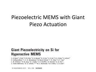
Piezoelectric MEMS with Giant
       Piezo Actuation
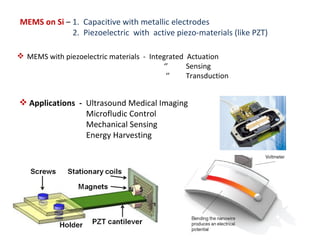
MEMS on Si – 1. Capacitive with metallic electrodes
             2. Piezoelectric with active piezo-materials (like PZT)

 MEMS with piezoelectric materials - Integrated Actuation
                                          ‘’     Sensing
                                           ‘’    Transduction


 Applications - Ultrasound Medical Imaging
                 Microfludic Control
                 Mechanical Sensing
                 Energy Harvesting
Piezoelectricity
    “Piezo” – Pressure; Piezo-electricity - pressure electricity

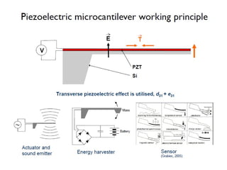
    Direct and Converse piezoelectric effect

Important Piezoelectric Parameters
Piezoelectric Figure of Merit
  Piezoelectric Strain Constant (d) – Magnitude of the induced strain (x) by an external
  electric field.   x= d.E

  Piezoelectric Voltage constant (g) – field per unit strain.
                                      g =d/(εε0) ;            ε= permittivity

  Electromechanical Coupling Factor (k) – Conversion rate between elec. & mech. energy.
                       = (stored elec. Energy)/(Input mech. Energy)
                        = d2/ (εε0).s

  Energy Transmission Coefficient (λ) – Maximum k in actual device
                                      = ʃ E.dp = (εε0E + d.x)E

  Efficiency (Ƞ) - (output mech. Energy)/(Consumed elec. Energy)
Displacement and Stress/Strain relation (at low fields)


Clamping to the Substrate changes it all !!


 31 and 33 modes of piezoresponse
Piezoelectric Properties of representative materials
MEMS Based on PbZr(1-x)Tix03

                                                     Interesting Properties at MPB –
                                                     2.High Dielectric Susceptibility
                                                     3.High Remnant Polarization
                                                     4.High Piezoelectric Coefficient


Pertinent issues encountered while integrating on Si –
1. Suitable buffer layer owing to higher lattice mismatch.
2. Suitable bottom electrode maintaining epitaxial nature .
3. Suitable growth condition leading to defect-minimal interface.
MEMS Based on PZT
Earlier Works   Appl. Phys. Lett., Vol. 74, No. 23, 7
Appl. Phys. Lett. 68 (10)
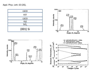
Appl. Phys. Lett. 63 (26),

                      LSCO
                      PZT
                      LSCO
                       YSZ
                       SiO2

                   (001) Si
Appl. Phys. Lett. 63 , 189
Appl. Phys. Lett., Vol. 76, No. 11, 13


Electron Diffraction Patterns


      PZT/YBCO             YBCO/MgO       STO/MgO   TiN/Si
J. Micromech. Microeng. 20 (2010) 055008


    Process Flow for MEMS Micro-fabrication


                                              Hysteresis Loop
PZT Membrane   PZT Cantilever
MEMS with Giant Piezo Coefficients


Problem with Giant Piezo MEMS – Relaxor materials are difficult
to integrate in Si matrix for device fabrication
PMN:25%PT
 PMN:33%PT
 PYN:46%PT

PZT
Giant Piezoelectricity for Hyperactive MEMS

Material: PMN:33%PT
Orientation : (001) {according to S. E. Park, T. R. Shrout, J. Appl. Phys. 82, 1804 (1997)}

Problem : Growth of Pyrochlore Phase.

Approaches : 1) The use of SrTiO3 buffer layer.
            2) a high miscut in Si substrate.
               (To incormorate volatile components in the film like PbO suppressing
                formation of pyrochlore)


        Zero Miscut               4o miscut
HRTEM at the Interface


   Atomically sharp interfaces.

Dielectric and Ferroelectric Measurement


   Existence of a built-in-bias – advantages and drawbacks.
Piezoresponse


Possible reason of higher piezo-activity- 1. Substantial self-polarization
                                         2. Built in bias


 Highest e31,f measured after poling = -27 +/- 3 c/m2
How far the properties hold w.r.t. microfabrication ?


 Fabrication
Cantilever deflection with external bias
Conclusions
      Epitaxial growth of PMN-PT on (001)Si using STO buffer.
      Improved growth through introduction of a high miscut in Si.
      Manifestation of giant piezoelectric properties.
      Higher figure of merit suitable for device integration.
      Preserved properties after microfabrocation.


Coda and Future Challenges
     High piezo-actuation through use of relaxors may enhance device sensitivity
     Denser device integration in IC – actuator arrays through easing downscaling.
     Low power consumption owing to reduction in actuation charge density.
     Smaller electromechanical devices with better performances.

  Exploitation of higher 33 mode response of PMN-PT rather 31 mode.
  Tuning the elastic properties of passive layers (SiO2, electrode, STO)to
   enhance in figure of merit further.
  Using SOI for complex device structures with desired passive layer thickness.
  Beyond EMS devices – tune and modulate multifunctional properties with
   giant electrostriction and dynamic strain control.

Piezoelectric mems

  • 1.
    Piezoelectric MEMS withGiant Piezo Actuation
  • 2.
    MEMS on Si– 1. Capacitive with metallic electrodes 2. Piezoelectric with active piezo-materials (like PZT)  MEMS with piezoelectric materials - Integrated Actuation ‘’ Sensing ‘’ Transduction  Applications - Ultrasound Medical Imaging Microfludic Control Mechanical Sensing Energy Harvesting
  • 3.
    Piezoelectricity  “Piezo” – Pressure; Piezo-electricity - pressure electricity  Direct and Converse piezoelectric effect Important Piezoelectric Parameters Piezoelectric Figure of Merit Piezoelectric Strain Constant (d) – Magnitude of the induced strain (x) by an external electric field. x= d.E Piezoelectric Voltage constant (g) – field per unit strain. g =d/(εε0) ; ε= permittivity Electromechanical Coupling Factor (k) – Conversion rate between elec. & mech. energy. = (stored elec. Energy)/(Input mech. Energy) = d2/ (εε0).s Energy Transmission Coefficient (λ) – Maximum k in actual device = ʃ E.dp = (εε0E + d.x)E Efficiency (Ƞ) - (output mech. Energy)/(Consumed elec. Energy)
  • 4.
    Displacement and Stress/Strainrelation (at low fields) Clamping to the Substrate changes it all !! 31 and 33 modes of piezoresponse
  • 5.
    Piezoelectric Properties ofrepresentative materials
  • 6.
    MEMS Based onPbZr(1-x)Tix03 Interesting Properties at MPB – 2.High Dielectric Susceptibility 3.High Remnant Polarization 4.High Piezoelectric Coefficient Pertinent issues encountered while integrating on Si – 1. Suitable buffer layer owing to higher lattice mismatch. 2. Suitable bottom electrode maintaining epitaxial nature . 3. Suitable growth condition leading to defect-minimal interface.
  • 7.
    MEMS Based onPZT Earlier Works Appl. Phys. Lett., Vol. 74, No. 23, 7
  • 8.
  • 9.
    Appl. Phys. Lett.63 (26), LSCO PZT LSCO YSZ SiO2 (001) Si
  • 10.
  • 11.
    Appl. Phys. Lett.,Vol. 76, No. 11, 13 Electron Diffraction Patterns PZT/YBCO YBCO/MgO STO/MgO TiN/Si
  • 13.
    J. Micromech. Microeng.20 (2010) 055008 Process Flow for MEMS Micro-fabrication Hysteresis Loop
  • 14.
    PZT Membrane PZT Cantilever
  • 15.
    MEMS with GiantPiezo Coefficients Problem with Giant Piezo MEMS – Relaxor materials are difficult to integrate in Si matrix for device fabrication
  • 17.
  • 18.
    Giant Piezoelectricity forHyperactive MEMS Material: PMN:33%PT Orientation : (001) {according to S. E. Park, T. R. Shrout, J. Appl. Phys. 82, 1804 (1997)} Problem : Growth of Pyrochlore Phase. Approaches : 1) The use of SrTiO3 buffer layer. 2) a high miscut in Si substrate. (To incormorate volatile components in the film like PbO suppressing formation of pyrochlore) Zero Miscut 4o miscut
  • 19.
    HRTEM at theInterface  Atomically sharp interfaces. Dielectric and Ferroelectric Measurement  Existence of a built-in-bias – advantages and drawbacks.
  • 20.
    Piezoresponse Possible reason ofhigher piezo-activity- 1. Substantial self-polarization 2. Built in bias Highest e31,f measured after poling = -27 +/- 3 c/m2
  • 21.
    How far theproperties hold w.r.t. microfabrication ? Fabrication
  • 22.
  • 23.
    Conclusions  Epitaxial growth of PMN-PT on (001)Si using STO buffer.  Improved growth through introduction of a high miscut in Si.  Manifestation of giant piezoelectric properties.  Higher figure of merit suitable for device integration.  Preserved properties after microfabrocation. Coda and Future Challenges  High piezo-actuation through use of relaxors may enhance device sensitivity  Denser device integration in IC – actuator arrays through easing downscaling.  Low power consumption owing to reduction in actuation charge density.  Smaller electromechanical devices with better performances.  Exploitation of higher 33 mode response of PMN-PT rather 31 mode.  Tuning the elastic properties of passive layers (SiO2, electrode, STO)to enhance in figure of merit further.  Using SOI for complex device structures with desired passive layer thickness.  Beyond EMS devices – tune and modulate multifunctional properties with giant electrostriction and dynamic strain control.