Download as PDF, PPTX


![/amradelm
Variations in interconnect
Temperature variations
on chip [2]
Sources of OCV
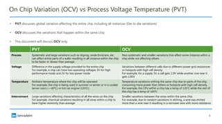
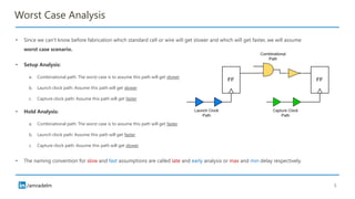
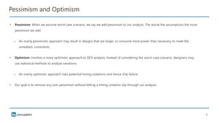
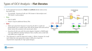
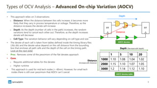
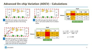
• Process Variations: Variations in the manufacturing process can lead to
differences in transistor characteristics (such as threshold voltage, oxide
thickness, doping concentration, etc.)
• Temperature Variations: Temperature fluctuations across the chip during
operation can cause variations in transistor behaviour and interconnect delays.
• Supply Voltage Variations: Fluctuations in the supply voltage, due to factors like
power supply noise or voltage drop, can affect the performance of transistors
and circuits.
• Interconnect Variations: Variations in interconnect resistance, capacitance, and
parasitic effects can lead to differences in signal propagation delay and power
consumption
MOSFET under microscope [1]
3](https://image.slidesharecdn.com/onchipvariationocv-241012070911-b1d156c9/85/VLSI-Static-Timing-Analysis-Timing-Checks-Part-5-On-Chip-Variation-3-320.jpg)


![/amradelm
Citations
• [1] https://www.bbvaopenmind.com/en/technology/innovation/mini-transistors-technological-revolution-20th-century/
• [2] L. Chen, W. Jin and S. X. . -D. Tan, "Fast Thermal Analysis for Chiplet Design based on Graph Convolution Networks," 2022 27th
Asia and South Pacific Design Automation Conference (ASP-DAC), Taipei, Taiwan, 2022, pp. 485-492, doi: 10.1109/ASP-
DAC52403.2022.9712583.](https://image.slidesharecdn.com/onchipvariationocv-241012070911-b1d156c9/85/VLSI-Static-Timing-Analysis-Timing-Checks-Part-5-On-Chip-Variation-22-320.jpg)


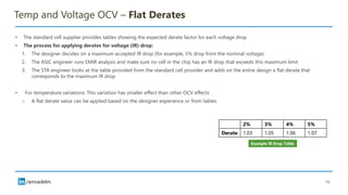
The document discusses on-chip variation (OCV), which arises from various factors like manufacturing process variations, temperature fluctuations, and voltage supply differences, affecting the performance of integrated circuits. It distinguishes OCV from global variations and explains approaches for analyzing OCV, including pessimistic and optimistic strategies, flat derates, advanced on-chip variation (AOCV), and parametric on-chip variation (POCV). The goal of these analyses is to balance design safety with performance efficiency while addressing specific challenges posed by variations within integrated circuits.


![[Back2School] STA Methodology- Chapter 7pdf](https://cdn.slidesharecdn.com/ss_thumbnails/stamethodology-250624214856-5fd24ebc-thumbnail.jpg?width=640&height=640&fit=bounds)