Downloaded 27 times

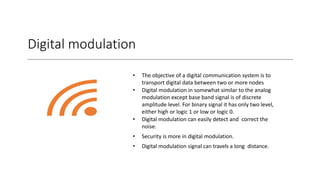
![Amplitude Shift Keying (ASK)
• As information signal is of binary
format, only two voltage levels
occur at input (either +1V or -1V)
• As a result, we get only two voltage
levels at output (either [Ac cos(ωct)
] or OV)
• Because of these two output voltage
levels, the carrier is either in “ON”
or “OFF” state.
• That’s the reason why ASK is also
known as “ON-OFF Keying (OOK)](https://image.slidesharecdn.com/phaseshiftkeying-190601002043/85/Phase-shift-keying-6-320.jpg)
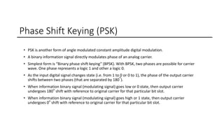
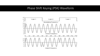
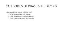
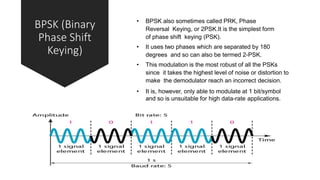

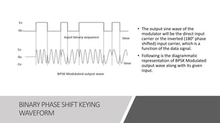
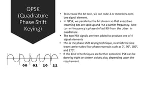
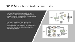
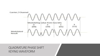
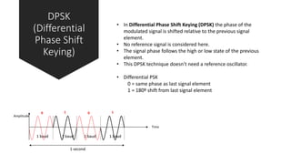
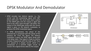
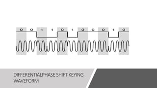
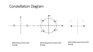

Phase Shift Keying (PSK) is a digital modulation technique that encodes data by manipulating the phase of a carrier wave. There are three main types of PSK: BPSK uses two phases separated by 180 degrees to represent 1 and 0; QPSK uses four phases separated by 90 degrees to represent 2 bits per symbol; DPSK shifts the phase relative to the previous symbol by 0 or 180 degrees without a reference carrier. PSK is commonly used in optical communications systems due to its efficiency and noise resistance.