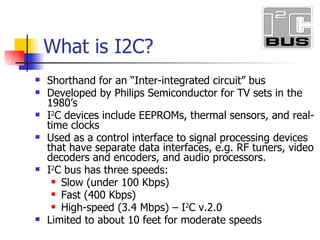
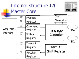
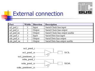
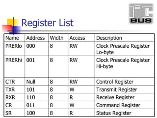
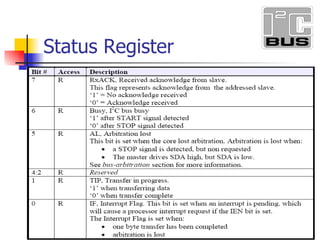
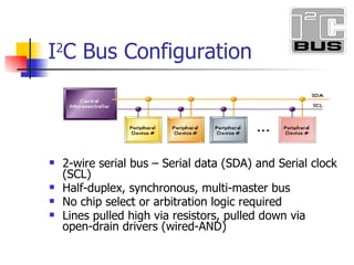
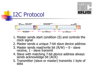
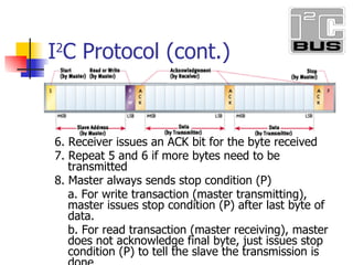
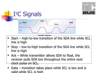
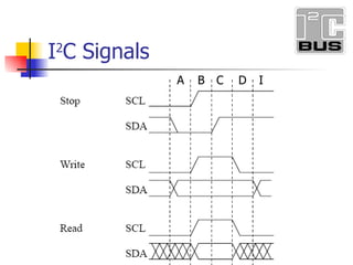
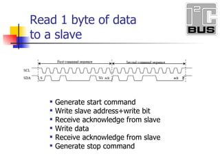
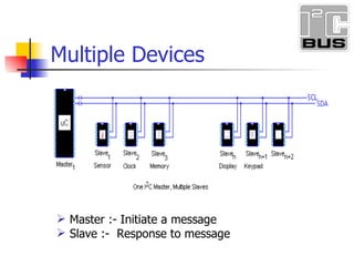
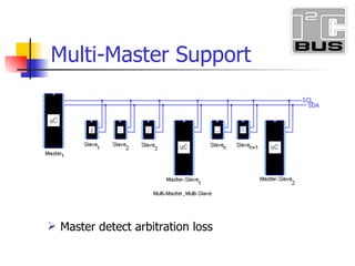
Mr.Tejas Dave Chovatiya Ravi Jitendra Edle Sachin Nigam Prepared by:- Guide by:- “ I2C Bus Protocol Implementation” THAKUR INSTITUTE OF CAREER ADVANCEMENT
Shorthand for an “Inter-integrated circuit” bus Developed by Philips Semiconductor for TV sets in the 1980’s I 2 C devices include EEPROMs, thermal sensors, and real-time clocks Used as a control interface to signal processing devices that have separate data interfaces, e.g. RF tuners, video decoders and encoders, and audio processors. I 2 C bus has three speeds: Slow (under 100 Kbps) Fast (400 Kbps) High-speed (3.4 Mbps) – I 2 C v.2.0 Limited to about 10 feet for moderate speeds What is I2C?
Addr 000 Addr 001 Addr 011 Addr 100 Addr 101 Addr 110 SDA SCL Internal structure I2C  Master Core  WISHBORN Interface Prescale  Register Command Register Transmit Register Status  Register Receiver Register Data IO Shift Register Bit & Byte Controller Clock Generator
External connection
Register List Status Register R 8 100 SR Command Register W 8 011 CR Receive Register R 8 110 RXR Transmit Register W 8 101 TXR Control Register RW 8 Null CTR Clock Prescale Register Hi-byte RW 8 001 PRERhi Clock Prescale Register Lo-byte RW 8 000 PRERlo Description Access Width Address Name
  Control register
Transmit Register Receive Register
Command Register
Status Register
I 2 C Bus Configuration 2-wire serial bus – Serial data (SDA) and Serial clock (SCL) Half-duplex, synchronous, multi-master bus No chip select or arbitration logic required Lines pulled high via resistors, pulled down via open-drain drivers (wired-AND)
I2C Protocol  1. Master sends start condition (S) and controls the clock signal 2. Master sends a unique 7-bit slave device address 3. Master sends read/write bit (R/W) – 0 - slave receive, 1 - slave transmit 4. Slave with matching 7-bit device address always sends acknowledge bit (ACK)  5. Transmitter (slave or master) transmits 1 byte of data
I 2 C Protocol (cont.) 6. Receiver issues an ACK bit for the byte received 7. Repeat 5 and 6 if more bytes need to be transmitted 8. Master always sends stop condition (P) a. For write transaction (master transmitting), master issues stop condition (P) after last byte of data. b. For read transaction (master receiving), master does not acknowledge final byte, just issues stop condition (P) to tell the slave the transmission is done
Start – high-to-low transition of the SDA line while SCL line is high Stop – low-to-high transition of the SDA line while SCL line is high Ack – While transmitter allows SDA to float, the receiver pulls SDA low throughout the entire next clock pulse on SCL. Data – transition takes place while SCL is low and is valid while SCL is high I 2 C Signals
  Bit Command Controller I
A B I 2 C Signals C D I
Write 1 byte of data  to a slave Generate start command Write slave address+write bit Receive acknowledge from slave Write data Receive acknowledge from slave Generate stop command
Read 1 byte of data  to a slave  Generate start command Write slave address+write bit Receive acknowledge from slave Write data Receive acknowledge from slave Generate stop command
Receive acknowledge from slave Generate repeated start signal Write slave address + read bit Receive acknowledge from slave Read byte from slave Write no acknowledge to slave,indicationg end of transfer Generate stop signal
I 2 C Features “ Clock stretching” – when the receiver needs more time to process a bit, it can pull SCL low to keep it from going high a bit longer. This technique is called clock stretching .   On SDL low, the transmitter can send its next data value, but this value will not be interpreted as a valid data symbol by the receiver until after the slave is ready to release SCL to go high. “ General call” broadcast – addresses every device on the bus 10-bit extended addressing for new designs.  7-bit addresses all exhausted
Clock Synchronization If two or more masters simultaneously try to control the bus, a clock synchronization procedure determines the bus clock.  Because of the wired-AND connection of the I2C signals a high to low transition affects all devices connected to the bus.
Master :- Initiate a message  Slave :-  Response to message Multiple Devices
Master detect arbitration loss Multi-Master Support
Reduce IC Pins, Cost and Area  Reduce PCB Size And Cost Advantages Of I2C
Addr 000 Addr 001 Addr 011 Addr 100 Addr 101 Addr 110 SDA SCL Internal structure I2C  Master Core  WISHBORN Interface Prescale  Register Command Register Transmit Register Status  Register Receiver Register Data IO Shift Register Bit & Byte Controller Clock Generator
References I 2 C: http://www-us2.semiconductors.philips.com/acrobat/various/ I2C_BUS_SPECIFICATION_1995.pdf http://www.esacademy.com/faq/i2c/index.htm http://www.embedded.com/story/OEG20020528S0057
Thank you

I2C

  • 1.
    Mr.Tejas Dave ChovatiyaRavi Jitendra Edle Sachin Nigam Prepared by:- Guide by:- “ I2C Bus Protocol Implementation” THAKUR INSTITUTE OF CAREER ADVANCEMENT
  • 2.
    Shorthand for an“Inter-integrated circuit” bus Developed by Philips Semiconductor for TV sets in the 1980’s I 2 C devices include EEPROMs, thermal sensors, and real-time clocks Used as a control interface to signal processing devices that have separate data interfaces, e.g. RF tuners, video decoders and encoders, and audio processors. I 2 C bus has three speeds: Slow (under 100 Kbps) Fast (400 Kbps) High-speed (3.4 Mbps) – I 2 C v.2.0 Limited to about 10 feet for moderate speeds What is I2C?
  • 3.
    Addr 000 Addr001 Addr 011 Addr 100 Addr 101 Addr 110 SDA SCL Internal structure I2C Master Core WISHBORN Interface Prescale Register Command Register Transmit Register Status Register Receiver Register Data IO Shift Register Bit & Byte Controller Clock Generator
  • 4.
  • 5.
    Register List StatusRegister R 8 100 SR Command Register W 8 011 CR Receive Register R 8 110 RXR Transmit Register W 8 101 TXR Control Register RW 8 Null CTR Clock Prescale Register Hi-byte RW 8 001 PRERhi Clock Prescale Register Lo-byte RW 8 000 PRERlo Description Access Width Address Name
  • 6.
    Controlregister
  • 7.
  • 8.
  • 9.
  • 10.
    I 2 CBus Configuration 2-wire serial bus – Serial data (SDA) and Serial clock (SCL) Half-duplex, synchronous, multi-master bus No chip select or arbitration logic required Lines pulled high via resistors, pulled down via open-drain drivers (wired-AND)
  • 11.
    I2C Protocol 1. Master sends start condition (S) and controls the clock signal 2. Master sends a unique 7-bit slave device address 3. Master sends read/write bit (R/W) – 0 - slave receive, 1 - slave transmit 4. Slave with matching 7-bit device address always sends acknowledge bit (ACK) 5. Transmitter (slave or master) transmits 1 byte of data
  • 12.
    I 2 CProtocol (cont.) 6. Receiver issues an ACK bit for the byte received 7. Repeat 5 and 6 if more bytes need to be transmitted 8. Master always sends stop condition (P) a. For write transaction (master transmitting), master issues stop condition (P) after last byte of data. b. For read transaction (master receiving), master does not acknowledge final byte, just issues stop condition (P) to tell the slave the transmission is done
  • 13.
    Start – high-to-lowtransition of the SDA line while SCL line is high Stop – low-to-high transition of the SDA line while SCL line is high Ack – While transmitter allows SDA to float, the receiver pulls SDA low throughout the entire next clock pulse on SCL. Data – transition takes place while SCL is low and is valid while SCL is high I 2 C Signals
  • 14.
    BitCommand Controller I
  • 15.
    A B I2 C Signals C D I
  • 16.
    Write 1 byteof data to a slave Generate start command Write slave address+write bit Receive acknowledge from slave Write data Receive acknowledge from slave Generate stop command
  • 17.
    Read 1 byteof data to a slave Generate start command Write slave address+write bit Receive acknowledge from slave Write data Receive acknowledge from slave Generate stop command
  • 18.
    Receive acknowledge fromslave Generate repeated start signal Write slave address + read bit Receive acknowledge from slave Read byte from slave Write no acknowledge to slave,indicationg end of transfer Generate stop signal
  • 19.
    I 2 CFeatures “ Clock stretching” – when the receiver needs more time to process a bit, it can pull SCL low to keep it from going high a bit longer. This technique is called clock stretching . On SDL low, the transmitter can send its next data value, but this value will not be interpreted as a valid data symbol by the receiver until after the slave is ready to release SCL to go high. “ General call” broadcast – addresses every device on the bus 10-bit extended addressing for new designs. 7-bit addresses all exhausted
  • 20.
    Clock Synchronization Iftwo or more masters simultaneously try to control the bus, a clock synchronization procedure determines the bus clock. Because of the wired-AND connection of the I2C signals a high to low transition affects all devices connected to the bus.
  • 21.
    Master :- Initiatea message Slave :- Response to message Multiple Devices
  • 22.
    Master detect arbitrationloss Multi-Master Support
  • 23.
    Reduce IC Pins,Cost and Area Reduce PCB Size And Cost Advantages Of I2C
  • 24.
    Addr 000 Addr001 Addr 011 Addr 100 Addr 101 Addr 110 SDA SCL Internal structure I2C Master Core WISHBORN Interface Prescale Register Command Register Transmit Register Status Register Receiver Register Data IO Shift Register Bit & Byte Controller Clock Generator
  • 25.
    References I 2C: http://www-us2.semiconductors.philips.com/acrobat/various/ I2C_BUS_SPECIFICATION_1995.pdf http://www.esacademy.com/faq/i2c/index.htm http://www.embedded.com/story/OEG20020528S0057
  • 26.