A photodiode is a semiconductor device that converts light into electrical current. It is a type of light sensor that operates based on the photoelectric effect, which means that when light falls on the photodiode, it generates electron-hole pairs, producing a current proportional to the intensity of the light.
![Responsivity
• The primary photocurrent resulting from absorption is:
• Quantum Efficiency:
• Responsivity:
)
1
)(
1
( )
(
0 f
w
p R
e
P
h
q
I s
[6-3]
h
P
q
IP
/
/
photons
incident
of
#
pairs
ated
photogener
hole
-
electron
of
#
0
[6-4]
[A/W]
0
h
q
P
I P
[6-5]](https://image.slidesharecdn.com/mywork-250625162143-e54e9a3c/85/photodiode-is-a-semiconductor-device-that-converts-2-320.jpg)
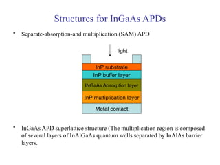
![Responsivity of APD
• The multiplication factor (current gain) M for all carriers generated in the
photodiode is defined as:
• Where is the average value of the total multiplied output current &
is the primary photocurrent.
• The responsivity of APD can be calculated by considering the current gain
as:
p
M
I
I
M [6-6]
M
I P
I
M
M
h
q
0
APD
[6-7]](https://image.slidesharecdn.com/mywork-250625162143-e54e9a3c/85/photodiode-is-a-semiconductor-device-that-converts-5-320.jpg)
![Signal Calculation
• Consider the modulated optical power signal P(t) falls on the photodetector
with the form of:
• Where s(t) is message electrical signal and m is modulation index.
Therefore the primary photocurrent is (for pin photodiode M=1):
• The root mean square signal current is then:
)]
(
1
[
)
( 0 t
ms
P
t
P
[6-8]
]
current
AC
)[
(
]
value
DC
[
)
(
ph t
i
I
t
MP
h
q
i p
P
[6-9]
signal
sinusoidal
for
2
2
2
2
2
2
2
2
2
P
p
p
s
p
s
I
m
i
M
i
i
[6-9]
[6-10]](https://image.slidesharecdn.com/mywork-250625162143-e54e9a3c/85/photodiode-is-a-semiconductor-device-that-converts-7-320.jpg)
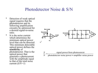
![Noise calculation (2)
• The total rms photodetector noise current is:
• The thermal noise of amplifier connected to the photodetector is:
input resistance of amplifier, and is Boltzmann
cte.
B
qI
M
F
BM
I
I
q
i
i
i
i
L
D
P
DS
DB
Q
N
N
2
)
(
)
(
2 2
2
2
2
2
2
[6-14]
L
B
T
T
R
TB
k
i
4
2
2
[6-15]
L
R -1
23
JK
10
38
.
1
B
k](https://image.slidesharecdn.com/mywork-250625162143-e54e9a3c/85/photodiode-is-a-semiconductor-device-that-converts-8-320.jpg)
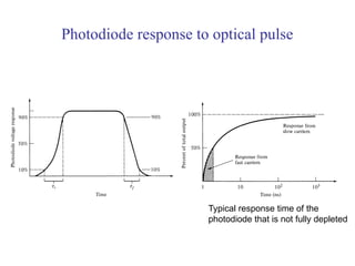
![Photodetector Response Time
• The response time of a photodetector with its output circuit depends
mainly on the following three factors:
1- The transit time of the photocarriers in the depletion region. The transit
time depends on the carrier drift velocity and the depletion layer
width w, and is given by:
2- Diffusion time of photocarriers outside depletion region.
3- RC time constant of the circuit. The circuit after the photodetector acts
like RC low pass filter with a passband given by:
d
t d
v
d
d
v
w
t [6-18]
T
T C
R
B
2
1
[6-19]
d
a
T
L
s
T C
C
C
R
R
R
and
||](https://image.slidesharecdn.com/mywork-250625162143-e54e9a3c/85/photodiode-is-a-semiconductor-device-that-converts-9-320.jpg)