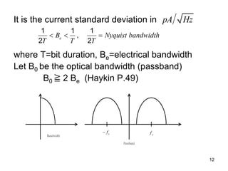
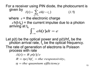
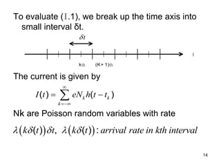
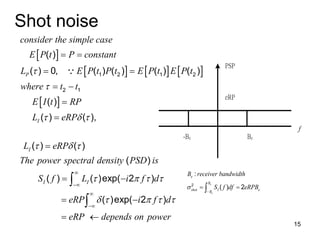
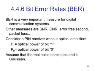
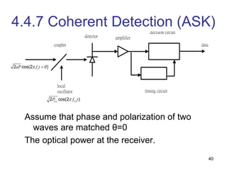
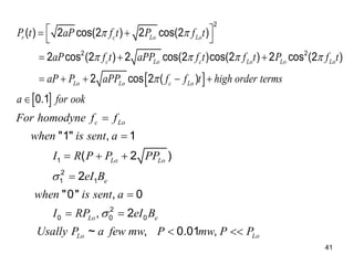
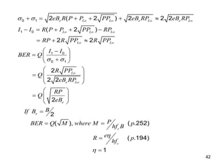
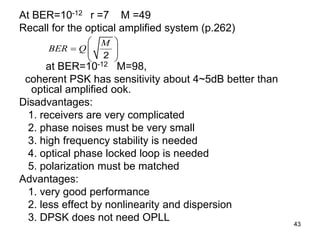
1
Chapter 4
Modulation and Demodulation
Modulation/Demodulation schemes,
Receiver design, Signal-to-noise ratio
(SNR), Bit error rate (BER)
2
4.1 Modulation
a. Intensity modulation/ Direct detection
i. digital (on- off keying, OOK)
ii. analog
b. Coherent modulation
3
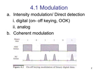
4.1.1 Signal format (digital)
a. Unipolar return-to-zero (RZ, x%)
b. Unipolar non-return-to-zero (NRZ)
i. need good DC balance
ii. For time recover circuits, transitions are
needed. (line coding or scrambling)
[(8,10) or (4,5) coding needs extra
bandwidth]
The NRZ format is very popular for high
speed communication systems (e.g.
10Gb/s)
4
4.4 Demodulation
BER ~ 10-9 or 10-12
3R: Regeneration, reshaping and retiming
5
4.4.1 An Ideal Receiver
It can be viewed as photon counting.
Direct detection is used with the following
assumptions
a. When any light is seen, the receiver makes in
favor of symbol “1”, otherwise it makes in favor
of symbol “o”
b. Photons will generate electron-hole pairs
randomly as a Poisson random process.
When “o” was sent, there is no light. For an ideal
receiver, it is error free.
When “1” was sent, because of Poisson random
process, if no electron-holes are generated the
receiver will make in favor of “o” => error
occurs
6
The photon arriving rate for a light pulse with power P is
P/hf
h: planck’s constant
= 6.63 x 10⁻³⁴ J-sec
hf: the energy of a single photon
Let B denote the bit rate,
the T = 1/B is the bit duration
Recall for Poisson process
P(λ) = exp(-λT) (λT)n /n!
where λ= P / hf (photon arriving rate)
The probability that n electron-hole pairs are generated
during T = 1/B seconds
P(λ) = exp(-P/hfB) (P/hfB)n /n!
7
If n≧1 we decide that the bit is “1” otherwise
it is “o” bit.
The probability the a light pulse does not
generate any electron-hole pair is
P(λ) = exp(-P/hfB)
Assuming that “1” and “o” are transmitted
with equal probability,
BER = ½ exp (-P/hfB) + ½ x 0
“1” “0”
8
Let M be the number of photons for “1” bit in
T seconds (M = P/hfB)
BER = ½ e-M
which is called the quantum limit
BER = 10-12 M = 27
BER = 10-9 M = 21 (BER = 7.6 x 10⁻¹⁰)
Practically the receiver has noise, more light
power is needed to achieve the same BER.
9
4.4.2 A Practical Direct Detection Receiver
10
11
The noise sources
a. thermal noise
b. shot noise
The thermal noise current in a resistor R at
temperate T can be modeled as Additive White
Gaussian Noise (AWGN) with zero mean and
variance 4KBT/R
KB = Boltzmann’s constance
=1.38 x 10⁻²³ J/Ko
Let Be be the signal bandwidth
The variance of the thermal noise is
 
2
2
4
thermal B e
t e
K T R B
I B
 

12
It is the current standard deviation in
where T=bit duration, Be=electrical bandwidth
Let B0 be the optical bandwidth (passband)
B0 ≧ 2 Be (Haykin P.49)
pA Hz
1 1 1
,
2 2
e
B Nyquist bandwidth
T T T
  
Bandwidth
Passband
c
f
 c
f
13
For a receiver using PIN diode, the photocurrent is
given by
where e = the electronic charge
e h(t-tk) = the current impulse due to a photon
arriving at tk
Let p(t) be the optical power and p(t)/hfc be the
photon arrival rate, fc be the optical frequency.
The rate of generation of electrons is Poisson
process with rate
( ) ( ) ( .1)
k
k
k
I t eh t t I

 

( )
eh t dt e




( ) ( )
,
c
t R p t e
R e hf the responsivity
the quantum efficiency




 

14
To evaluate (I.1), we break up the time axis into
small interval δt.
The current is given by
Nk are Poisson random variables with rate
( ) ( )
k k
k
I t eN h t t


 

   
( ) , ( ) :
k t t k t arrival rate in kth interval
    
t
t

kth (K+ 1)th
15
Shot noise
 
     
 
1 2 1 2
2 1
( )
( ) 0, ( ) ( ) ( ) ( )
( )
( ) ( ),
( ) ( )
( )
( ) ( )exp( 2 )
( )exp( 2 )
P
I
I
I I
consider the simple case
E P t P constant
L E P t P t E P t E P t
where t t
E I t RP
L eRP
L eRP
The power spectral density PSD is
S f L i f d
eRP i f d


  
  
   
    




 
 
 



 
 


eRP depends on power
 
PSP
eRP
-Be Be
f
2
:
( ) 2
e
e
e
B
shot I e
B
B receiver bandwidth
S f df eRPB


 

16
The photocurrent is given by
is the shot current with zero mean and
variance
s
I I i
I RP
 

s
i
2 e
eRPB
2
2
shot e
I RP
eIB



17
Let the local resistance be RL
The total current in the resistor is
Where is the thermal current with variance
Assume and are independent, the total
current has mean and variance
Note that is proportional to
there is a trade-off between SNR and
For IM/DD receivers
noiseless amplifier
RL
I
s t
I I i i
  
t
i
2 2
(4 / )
T
thermal B L e t e
K R B I B
  
t
i
s
i
I 2

2 2 2
shot thermal
  
 
2
 e
B
e
B
thermal shot
 
18
4.4.3 Front end amplifier noise
Define Noise Figure (Fn) of the amplifier
=(SNR)in / (SNR)out
typically Fn = 3~5dB
The thermal noise contribution is
Similary
2 4 B e n
thermal
L
K TB F
R
 
2
2
shot e n
eIB F
 
19
4.4.3 APD Noise
20
Gm(t): Gm
= Avalanche multiplication gain
will be amplified
Let RAPD=responsivity of APD
The average APD photocurrent is
The variance of shot noise is
FA(Gm): the excess noise factor
FA(Gm) = KAGm + (1 - KA)(2 -1 / Gm)
KA: ionization coefficient ratio
For silicon KA<<1
For InGaAs KA=0.7
Note if Gm=1, FA=1 (4.4) is the variance of shot noise of
PIN
2
shot

APD m
I R P G RP
 
2 2
2 ( ) (4.4)
shot m A m e
G F G RPB
 
21
4.4.5 Optical PreAmplifiers
The Amplified Spontaneous Emission (ASE) noise is the
main noise source of optical amplifiers.
The ASE noise power for each polarization is
Where nsp: the spontaneous emission factor
G: the amplifier gain
Bo: the optical bandwidth
nsp depends of level of population inversion, With
complete inversion nsp = 1
typically nsp = 2~5
0
( 1) (4.5)
N sp c
P n hf G B
 
22
There are two independent polarizations in a
single mode fiber
The total ASE noise power
P=2PN
Define
If the standard PIN is used
I=RGP (4.6)
R: responsivity
P: received power
0
, ( 1)
n sp c N n
P P
P n hf G B
  
23
Photocurrent I is proportional to the optical power
P which is proportional to the square of the
electrical field. Thus the noise field beats against
the signal and against itself. Thus signal-
spontaneous beat noise and spontaneous-
spontaneous beat noise are produced.
For Appendix I, we have
 
 
2 2
2
0
2 2
2
2 2
0
(4.7)
2 ( 1) (4.8)
4 ( 1) (4.9)
2 ( 1) (2 ) (4.10)
thermal t e
shot n e
signal spont n e
spont spont n e e
I B
eR GP P G B B
R PP G B
and R P G B B B







  
 
  
24
It is the received thermal noise current
If G is large (e.g > 10dB)
If Bo is small ≈ 2Be
Pn= nsphfc << P
is dominant, which can be modeled
as a Gaussian process.
2 4
,
B
t
K T
I R resistance
R
 
2 2 2 2
, ,
thermal shot sig spont spont spont
   
 
2 2
spont spont sig spont
 
 
2
sig sopnt
 
25
Recall (4.2)
At the amplifier input
At the amplifier output, using (4.6) and (4.9)
we have
2
2
2 (4.2)
2
shot e
shot e
eIB
I RP
eRPB





2
( )
2
i
e
RP
SNR
eRPB

2 2
0
2 2
( ) 4 ( 1)
( ) 4 ( 1)
n e
e sp c
n sp c
SNR RGP R GPP G B
RGP R GP G B n hf
P n hf
 
 

26
The noise figure of the amplifier is
In the above derivation, we assume no coupling
losses. The input coupling loss will degrade Fn
0
2
2 2
( ) 2
, 1
( ) 4 ( 1)
2
n i
e
sp c e
sp c
F SNR SNR
RP RePB
G
RGP R PG G n hf B
n hf R e




, 1
2
2
1 2 3
4 ~ 7
c
c
n sp c
sp
sp n
n
e
Recall R if
hf
e
hf
F n hf R e
n
If n F dB
typically F dB
 
 



  

27
4.4.6 Bit Error Rates (BER)
BER is a very important measure for digital
communication systems.
Other measures are SNR, CNR, error free second,
packet loss…
Consider a PIN receiver without optical amplifiers
P1= optical power of bit “1”
P0= optical power of bit “0”
Assume that thermal noise dominates and is
Gaussian.
28
For bit “1”, the mean photocurrent is
The variance is
RL: load resistant
For bit “0”, the variance is
For ideal case P0=0 I0=0
1 1
I I RP
 
2
0 0
2 4
e B e L
eI B K TB R
  
2
1 1
2 4
e B e L
eI B K TB R
  
signal thermal noise
2
0 4 B e L
K TB R
 
receiver
power
amplifier
AGC
decision
cht
timing
cht
optical
signal
with
filter
data
I
29
Assume the decision threshold current is Ith
If I > Ith decision is made in favor of “1”
If I < Ith decision is made in favor of “0”
30
Assume that bits “1” and “0” are transmitted equally
likely
Problem 4.7
The threshold current is
1
(0) (1)
2
p p
 
(4.12)
0 1 1 0
0 1
th
I I
I
 
 



Q(x)
Q(x)=
2
2
2
2
2
2
2
1
2
1
(4.13)
2
2
( )
2
2
2 ( )
y
x
y
x
z
x
y
x
Define as
e dy
e dy
Note evfc x e dz
e dy
Q x




 




 








31
Then we have
P
P
1
1
0
0
0 1
1 0
th
th
I I
Q
I I
Q


 

    
 
 
 

    
 
 
 
 
0 1 1 0
0 1
0 1 1 1 0 1 1 0
1
0 1
1 1 0
0 1
1 1 0
1 0 1
0 1 1 0 0 0 1 0
0
0 1
0 1 0
0 1
0 1 0
0 0 1
th
th
th
th
th
Recall
I I
I
I I I I
I I
I I
I I I I
I I I I
I I
I I
I I I I
 
 
   
 

 
  
   
 

 
  



  
 




 


  
 




 


32
If “1” and “0” are transmitted equally likely
1 0
0 1
1 1
(0 1) (10)
2 2
(4.14)
BER P P
I I
Q
 
 
 

  

 
1
1 0
0 1
12 9
( )
10 , 7, 10 , 6
I I
let r Q BER
For BER r BER r
 

 

 

   
1 0
1 0 1 0
1 0
2
1
2 2 2
th
I I
Practically I
I I I I
BER Q Q
 


 
 
 
 
 
 
 
 
 
   
 
33
We may specify BER then calculate the received power
(BER=10-12)
Define: The receiver sensitivity as
Psens= The minimum average optical power for given
BER (e.g 10-12 )
It is also expressed as the number of photons per bit.
Recall page252
1
1
1 0
1
1
: "1"
:
, 0
2
2
2
c
sens
sens
sens
c
P
M
hf B
P optical power for
B the bit rate
P P
P ideally P
P P
P
M
hf B


 


34
1
1 0
0 1
0
1 0 1
0 1
2 2 2 2 2
0 1
2 2
1
( )
0,
2
( ) (4.6)
: 1
( )
(4.15)
2
,
,
2 ( )
sens
m
m m
sens
m
thermal thermal shot
shot m A m e
Recall r Q BER
I I
P
For I P
I r RPG
G APD gain G for PIN
r
P
RG
For APD shot noise is significant
Recall eG F G RPB
 
 
 
    






 
  



  

2
(4.4)
4 ( ) sens
m A m e
eG F G RP B

35
 
0 1
2
2 2 2
1
2
2
2
2
(4.15)
2
2
4 ( )
2 4
4 ( )
( )
(
therm
sens
m
sens
m
sens
therm m A m e
sens sens
m m therm
sens
m A m e
sens
m therm
m A m e
therm
sens e A m
m
r
P
G R
G RP
eG F G RP B
r
G RP G RP
eG F G RP B
r r
G RP
eG F G B
r r
r
P eB F G
R G
 
  





 
 
   
 
 
 
 
 
 
 
 
 
 
 
 
 
2 22 2
12
) (4.16)
: , 3
2
100 , 300 , ( )
1.24
4
1.656 10
1 10 , 7
e n
L
B
therm n e
L
m
r
B
Assume B Hz B bit rate F dB
A
R T K R
W
K T
F B BA
R
G BER r

 

 
    
  
  
36
(KA=0.7, Gm=10)
37
For a system with optical amplifier
2
0
2 2
1 0
0 1
2
4 ( 1) (4.9)
(4.6)
(4.14)
2 ( 1)
(4.18)
2 ( 1)
e sig spont
sig spont n e
n e
n e
B B dominates
R GPP G B
RGP
I I
BER Q
RGP
Q
R GPP G B
GP
Q
P G B


 



 

 

  

 
 
  
 

 
 
  
 

 
I
38
12
2
, 1,
2
1 1
2 ( 1) 2
1
2 ,
2 2
2
, 10 , 7
2
2( ) 98
~
~
sp n sp c c
e
n e n e
c n e
If G is large n P n hf hf
B
B
GP P
r
G P B P B
P
P
M M
hf B P B
M
M
BER Q For BER r
M r M photons bit
practically M a few hundred photons bit
If optical amplifier is not used
M a f

  

 

  

 
  
 
 
 
  
ew thousand photons bit
39
If systems with cascades of optical amplifiers, optical signal
consists of a lot of optical noise, and can be
ignored. The received optical noise power PASE
dominates.
Define
Optical signal-to-noise ratio (OSNR)=
Based on above equation, (4.6), (4.9), (4.10) and (4.14)
We have
For 2.5Gb/s system, Be=2 GHz, Bo= 36GHz, r=7
=> OSNR = 4.37 = 6.14 dB
A rule of thumb used by designers
OSNR ≈ 20dB because of dispersion and nonlinearity
rec
ASE
P
P
0
0
2 ( 1) (4.5)
2 ( 1) ( )
ASE sp c
n
P n hf G B
P G B two pols
 
 
0
2
1 1 4
e
B
OSNR
B
r
OSNR

 
n sp c
P n hf

thermal
 shot

40
4.4.7 Coherent Detection (ASK)
Assume that phase and polarization of two
waves are matched θ=0
The optical power at the receiver.
coupler
detector amplifier
decision circuit
timing circuit
data
local
oscillator
2 cos(2 )
c
aP f t
 

2 cos(2 )
Lo Lo
P f t

41
 
 
2
2 2
( ) 2 cos(2 ) 2 cos(2 )
2 cos (2 ) 2 cos(2 )cos(2 ) 2 cos (2 )
2 cos 2 ( )
0.1
r c Lo Lo
c Lo c Lo Lo Lo
Lo Lo c Lo
P t aP f t P f t
aP f t aPP f t f t P f t
aP P aPP f f t high order terms
a for ook
 
   

 
 
 
  
    

1
2
1 1
2
0 0 0
"1" , 1
( 2 )
2
"0" , 0
, 2
~ , 0.01 ,
c Lo
Lo Lo
e
Lo e
Lo Lo
For homodyne f f
when is sent a
I R P P PP
eI B
when is sent a
I RP eI B
Usally P a few mw P mw P P




  


 
 
42
0 1
1 0
1 0
0 1
2 ( 2 ) 2 2 2
( 2 )
2 2
2
2 2
2
2
( ), ( .252)
( .194)
1
e Lo Lo e Lo e Lo
Lo Lo Lo
Lo Lo
Lo
e Lo
e
e
c
c
eB R P P PP eB RP eB RP
I I R P P PP RP
RP R PP R PP
I I
BER Q
R PP
Q
eB RP
RP
Q
eB
B
If B
P
BER Q M where M p
hf B
e
R p
hf
 
 


     
    
  
 

  

 
 
  
 
 
 
  
 
 

 


43
At BER=10-12 r =7 M =49
Recall for the optical amplified system (p.262)
at BER=10-12 M=98,
coherent PSK has sensitivity about 4~5dB better than
optical amplified ook.
Disadvantages:
1. receivers are very complicated
2. phase noises must be very small
3. high frequency stability is needed
4. optical phase locked loop is needed
5. polarization must be matched
Advantages:
1. very good performance
2. less effect by nonlinearity and dispersion
3. DPSK does not need OPLL
2
M
BER Q
 
  
 
 
44
4.4.8 Timing Recovery
Timing circuit produces timing clock for the
decision circuit.
1. Inband timing
2. Outband timing
Reference: Alain Blancharal “Phase-Locked Loops”
John Wiley and Sons., 1976 Chapter3
45
General time domain equation
Consider sinusoidal input and output
 
 
0 0
( ) sin ( )
( ) cos ( )
i i
y t A wt t
y t B wt t


 
 
VCO
i
y phase detector
1
u
loop filter
amplifier gain K2
2
u
0
y
clock
signal
0
3 2
d
k u
dt


46
For sinusoidal type phase detector
1
u
ideal

 
0
1 1 0
( ) ( )
( ) sin ( ) ( )
i
i
t t
u t k t t
  
 
 
 
Sinusoidal
47
Let F(iw) be the loop filter transfer function
and f(t) be its impulse response
 
 
 
 
     
   
2
2
2
2 2
2
1 1
2 2 1
2
2 2
2
2 1
2 ( ) 2
( ) 2
2 ( )
2 ( )
2 2 2
( ) ( 2 )
2 2
i ft
i ft
i ft
i ft
i ft
i ft
F i f f t e dt w f
f t F i f e df
U i f u t e dt
U i f u t e dt
U i f K U i f F i f
u t u i f e df
K U i f F i f e df






 



  

 















 












48
1
2 2
2 2 1
2 ( )
2 1
2
( ) ( ) ( 2 )
( ) ( 2 )
( ) ( )
i f i ft
i f t
u t K u e d F i f e d
K u F i f e dfd
K u f t d
  
 
   
  
  
 

 
 
 
 




 
 
 

2 2 1
( ) ( ) ( )
u t K u t f t
 
where * denotes the convolution operation
The output phase of the oscillator is
 
 
0
3 2
3 2 1
1 2 3 2
1 1 0
( )
( )
( ) ( )
sin ( ) ( ) ( )
( ) sin ( ) ( )
i
i
d t
K u t
dt
K K u t f t
K K K t t f t
u t K t t

 
 

 
  
 
convolution integral
49
 
 
 
1 2 3
0
0
0 0
0
0
0
2
0 0
2
0
( )
sin ( ) ( ) ( )
sin ( ) ( ) ( ) ( )
( ) ( )
( )
( ) ( ) ( )
( 2 ) ( )
( 2 ) ( )
(
i
i i
i
i
ft
ft
i i
let K K K K loop gain
d t
K t t f t
dt
Linearized equations
t t t t
when t t is small
d t
K t t f t
dt
let i f t e dt
i f t e dt
d t



 
   
 

 
 
 





 
  
  

  
 
 


2
0
2
0
0
)
( 2 )
2 ( 2 )
2 ( )
ft
ft
d
i f e df
dt dt
i f i f e df
i f t



 
 






 
  
 


50
 
 
 
0
0
0 0
0
0
( )
( ) ( ) ( )
( ) ( ) ( ) ( )
( ) ( ) ( ) ( )
( ) ( )
( )
( )
i
i
i
d t
Recall K t t f t
dt
Take Fourier Transform of both sides
iw iw K iw iw F iw
iw KF iw iw K iw F iw
The linearized transfer function of a phase locked loop is
iw KF iw
H iw
i iw iw

 
  
     
    


 
  
0
( )
( ) ( ) ( )
i
KF iw
The instantaneous phase error is
t t t
  
 
51
 
0
0
( ) ( ) ( )
( )
( )
( )
( ) ( ) ( ) ( )
1 ( ) ( )
( )
1 ( )
( ) ( )
( )
( )
( )
( )
1 ( )
( ) ( )
i
i
i i
i
i
i
iw iw iw
iw
Recall H iw
iw
iw iw H iw iw
H iw iw
iw iw
H iw
iw iw KF iw
let s iw
KF s
H s
s KF s
The error function is
s s
H s
s s KF s
    



    
  
 
  
  


 
 
  
  
52
0
0
0
0
0
0
0
( )
( ) 1
( )
( )( ) ( )
( )
( ) ( )
( )
1 ( )
( )
( )
( ) ( )
( ) ( ) ( )
i
i
i
i
i
For the first order loop all pass filter
F s
K
H s
s K
s s K K s
d
Recall iw s
dt
d t
K t K t
dt
s
s
Recall H s
s K s
d t d
K t t
dt dt
where t t t phase error

 

 
  


 
    
   
 


  
  
 
 
53
2
1
1
2
1
1 2
0
1
( )
1
( )
1
1
( )
1
, ,
( ) ( ) ( ) 0
( ) ( )
i
i
For the second order loops
s
F s
s
or F s
s
s
or F s
s
We adjust K to abtain
t t t at steady state
In normal operation
t changes with t





 
  
 








  
54
55
56
4.4.9 Equalization
The equalizer is used to reduce the effect of
intersymble interference (ISI) due to pulse
spreading caused by dispersion.

Chapter 4.ppt

  • 1.
    1 Chapter 4 Modulation andDemodulation Modulation/Demodulation schemes, Receiver design, Signal-to-noise ratio (SNR), Bit error rate (BER)
  • 2.
    2 4.1 Modulation a. Intensitymodulation/ Direct detection i. digital (on- off keying, OOK) ii. analog b. Coherent modulation
  • 3.
    3 4.1.1 Signal format(digital) a. Unipolar return-to-zero (RZ, x%) b. Unipolar non-return-to-zero (NRZ) i. need good DC balance ii. For time recover circuits, transitions are needed. (line coding or scrambling) [(8,10) or (4,5) coding needs extra bandwidth] The NRZ format is very popular for high speed communication systems (e.g. 10Gb/s)
  • 4.
    4 4.4 Demodulation BER ~10-9 or 10-12 3R: Regeneration, reshaping and retiming
  • 5.
    5 4.4.1 An IdealReceiver It can be viewed as photon counting. Direct detection is used with the following assumptions a. When any light is seen, the receiver makes in favor of symbol “1”, otherwise it makes in favor of symbol “o” b. Photons will generate electron-hole pairs randomly as a Poisson random process. When “o” was sent, there is no light. For an ideal receiver, it is error free. When “1” was sent, because of Poisson random process, if no electron-holes are generated the receiver will make in favor of “o” => error occurs
  • 6.
    6 The photon arrivingrate for a light pulse with power P is P/hf h: planck’s constant = 6.63 x 10⁻³⁴ J-sec hf: the energy of a single photon Let B denote the bit rate, the T = 1/B is the bit duration Recall for Poisson process P(λ) = exp(-λT) (λT)n /n! where λ= P / hf (photon arriving rate) The probability that n electron-hole pairs are generated during T = 1/B seconds P(λ) = exp(-P/hfB) (P/hfB)n /n!
  • 7.
    7 If n≧1 wedecide that the bit is “1” otherwise it is “o” bit. The probability the a light pulse does not generate any electron-hole pair is P(λ) = exp(-P/hfB) Assuming that “1” and “o” are transmitted with equal probability, BER = ½ exp (-P/hfB) + ½ x 0 “1” “0”
  • 8.
    8 Let M bethe number of photons for “1” bit in T seconds (M = P/hfB) BER = ½ e-M which is called the quantum limit BER = 10-12 M = 27 BER = 10-9 M = 21 (BER = 7.6 x 10⁻¹⁰) Practically the receiver has noise, more light power is needed to achieve the same BER.
  • 9.
    9 4.4.2 A PracticalDirect Detection Receiver
  • 10.
  • 11.
    11 The noise sources a.thermal noise b. shot noise The thermal noise current in a resistor R at temperate T can be modeled as Additive White Gaussian Noise (AWGN) with zero mean and variance 4KBT/R KB = Boltzmann’s constance =1.38 x 10⁻²³ J/Ko Let Be be the signal bandwidth The variance of the thermal noise is   2 2 4 thermal B e t e K T R B I B   
  • 12.
    12 It is thecurrent standard deviation in where T=bit duration, Be=electrical bandwidth Let B0 be the optical bandwidth (passband) B0 ≧ 2 Be (Haykin P.49) pA Hz 1 1 1 , 2 2 e B Nyquist bandwidth T T T    Bandwidth Passband c f  c f
  • 13.
    13 For a receiverusing PIN diode, the photocurrent is given by where e = the electronic charge e h(t-tk) = the current impulse due to a photon arriving at tk Let p(t) be the optical power and p(t)/hfc be the photon arrival rate, fc be the optical frequency. The rate of generation of electrons is Poisson process with rate ( ) ( ) ( .1) k k k I t eh t t I     ( ) eh t dt e     ( ) ( ) , c t R p t e R e hf the responsivity the quantum efficiency       
  • 14.
    14 To evaluate (I.1),we break up the time axis into small interval δt. The current is given by Nk are Poisson random variables with rate ( ) ( ) k k k I t eN h t t          ( ) , ( ) : k t t k t arrival rate in kth interval      t t  kth (K+ 1)th
  • 15.
    15 Shot noise          1 2 1 2 2 1 ( ) ( ) 0, ( ) ( ) ( ) ( ) ( ) ( ) ( ), ( ) ( ) ( ) ( ) ( )exp( 2 ) ( )exp( 2 ) P I I I I consider the simple case E P t P constant L E P t P t E P t E P t where t t E I t RP L eRP L eRP The power spectral density PSD is S f L i f d eRP i f d                                     eRP depends on power   PSP eRP -Be Be f 2 : ( ) 2 e e e B shot I e B B receiver bandwidth S f df eRPB     
  • 16.
    16 The photocurrent isgiven by is the shot current with zero mean and variance s I I i I RP    s i 2 e eRPB 2 2 shot e I RP eIB   
  • 17.
    17 Let the localresistance be RL The total current in the resistor is Where is the thermal current with variance Assume and are independent, the total current has mean and variance Note that is proportional to there is a trade-off between SNR and For IM/DD receivers noiseless amplifier RL I s t I I i i    t i 2 2 (4 / ) T thermal B L e t e K R B I B    t i s i I 2  2 2 2 shot thermal      2  e B e B thermal shot  
  • 18.
    18 4.4.3 Front endamplifier noise Define Noise Figure (Fn) of the amplifier =(SNR)in / (SNR)out typically Fn = 3~5dB The thermal noise contribution is Similary 2 4 B e n thermal L K TB F R   2 2 shot e n eIB F  
  • 19.
  • 20.
    20 Gm(t): Gm = Avalanchemultiplication gain will be amplified Let RAPD=responsivity of APD The average APD photocurrent is The variance of shot noise is FA(Gm): the excess noise factor FA(Gm) = KAGm + (1 - KA)(2 -1 / Gm) KA: ionization coefficient ratio For silicon KA<<1 For InGaAs KA=0.7 Note if Gm=1, FA=1 (4.4) is the variance of shot noise of PIN 2 shot  APD m I R P G RP   2 2 2 ( ) (4.4) shot m A m e G F G RPB  
  • 21.
    21 4.4.5 Optical PreAmplifiers TheAmplified Spontaneous Emission (ASE) noise is the main noise source of optical amplifiers. The ASE noise power for each polarization is Where nsp: the spontaneous emission factor G: the amplifier gain Bo: the optical bandwidth nsp depends of level of population inversion, With complete inversion nsp = 1 typically nsp = 2~5 0 ( 1) (4.5) N sp c P n hf G B  
  • 22.
    22 There are twoindependent polarizations in a single mode fiber The total ASE noise power P=2PN Define If the standard PIN is used I=RGP (4.6) R: responsivity P: received power 0 , ( 1) n sp c N n P P P n hf G B   
  • 23.
    23 Photocurrent I isproportional to the optical power P which is proportional to the square of the electrical field. Thus the noise field beats against the signal and against itself. Thus signal- spontaneous beat noise and spontaneous- spontaneous beat noise are produced. For Appendix I, we have     2 2 2 0 2 2 2 2 2 0 (4.7) 2 ( 1) (4.8) 4 ( 1) (4.9) 2 ( 1) (2 ) (4.10) thermal t e shot n e signal spont n e spont spont n e e I B eR GP P G B B R PP G B and R P G B B B               
  • 24.
    24 It is thereceived thermal noise current If G is large (e.g > 10dB) If Bo is small ≈ 2Be Pn= nsphfc << P is dominant, which can be modeled as a Gaussian process. 2 4 , B t K T I R resistance R   2 2 2 2 , , thermal shot sig spont spont spont       2 2 spont spont sig spont     2 sig sopnt  
  • 25.
    25 Recall (4.2) At theamplifier input At the amplifier output, using (4.6) and (4.9) we have 2 2 2 (4.2) 2 shot e shot e eIB I RP eRPB      2 ( ) 2 i e RP SNR eRPB  2 2 0 2 2 ( ) 4 ( 1) ( ) 4 ( 1) n e e sp c n sp c SNR RGP R GPP G B RGP R GP G B n hf P n hf     
  • 26.
    26 The noise figureof the amplifier is In the above derivation, we assume no coupling losses. The input coupling loss will degrade Fn 0 2 2 2 ( ) 2 , 1 ( ) 4 ( 1) 2 n i e sp c e sp c F SNR SNR RP RePB G RGP R PG G n hf B n hf R e     , 1 2 2 1 2 3 4 ~ 7 c c n sp c sp sp n n e Recall R if hf e hf F n hf R e n If n F dB typically F dB           
  • 27.
    27 4.4.6 Bit ErrorRates (BER) BER is a very important measure for digital communication systems. Other measures are SNR, CNR, error free second, packet loss… Consider a PIN receiver without optical amplifiers P1= optical power of bit “1” P0= optical power of bit “0” Assume that thermal noise dominates and is Gaussian.
  • 28.
    28 For bit “1”,the mean photocurrent is The variance is RL: load resistant For bit “0”, the variance is For ideal case P0=0 I0=0 1 1 I I RP   2 0 0 2 4 e B e L eI B K TB R    2 1 1 2 4 e B e L eI B K TB R    signal thermal noise 2 0 4 B e L K TB R   receiver power amplifier AGC decision cht timing cht optical signal with filter data I
  • 29.
    29 Assume the decisionthreshold current is Ith If I > Ith decision is made in favor of “1” If I < Ith decision is made in favor of “0”
  • 30.
    30 Assume that bits“1” and “0” are transmitted equally likely Problem 4.7 The threshold current is 1 (0) (1) 2 p p   (4.12) 0 1 1 0 0 1 th I I I        Q(x) Q(x)= 2 2 2 2 2 2 2 1 2 1 (4.13) 2 2 ( ) 2 2 2 ( ) y x y x z x y x Define as e dy e dy Note evfc x e dz e dy Q x                    
  • 31.
    31 Then we have P P 1 1 0 0 01 1 0 th th I I Q I I Q                               0 1 1 0 0 1 0 1 1 1 0 1 1 0 1 0 1 1 1 0 0 1 1 1 0 1 0 1 0 1 1 0 0 0 1 0 0 0 1 0 1 0 0 1 0 1 0 0 0 1 th th th th th Recall I I I I I I I I I I I I I I I I I I I I I I I I I I I                                                         
  • 32.
    32 If “1” and“0” are transmitted equally likely 1 0 0 1 1 1 (0 1) (10) 2 2 (4.14) BER P P I I Q              1 1 0 0 1 12 9 ( ) 10 , 7, 10 , 6 I I let r Q BER For BER r BER r              1 0 1 0 1 0 1 0 2 1 2 2 2 th I I Practically I I I I I BER Q Q                            
  • 33.
    33 We may specifyBER then calculate the received power (BER=10-12) Define: The receiver sensitivity as Psens= The minimum average optical power for given BER (e.g 10-12 ) It is also expressed as the number of photons per bit. Recall page252 1 1 1 0 1 1 : "1" : , 0 2 2 2 c sens sens sens c P M hf B P optical power for B the bit rate P P P ideally P P P P M hf B      
  • 34.
    34 1 1 0 0 1 0 10 1 0 1 2 2 2 2 2 0 1 2 2 1 ( ) 0, 2 ( ) (4.6) : 1 ( ) (4.15) 2 , , 2 ( ) sens m m m sens m thermal thermal shot shot m A m e Recall r Q BER I I P For I P I r RPG G APD gain G for PIN r P RG For APD shot noise is significant Recall eG F G RPB                              2 (4.4) 4 ( ) sens m A m e eG F G RP B 
  • 35.
    35   0 1 2 22 2 1 2 2 2 2 (4.15) 2 2 4 ( ) 2 4 4 ( ) ( ) ( therm sens m sens m sens therm m A m e sens sens m m therm sens m A m e sens m therm m A m e therm sens e A m m r P G R G RP eG F G RP B r G RP G RP eG F G RP B r r G RP eG F G B r r r P eB F G R G                                             2 22 2 12 ) (4.16) : , 3 2 100 , 300 , ( ) 1.24 4 1.656 10 1 10 , 7 e n L B therm n e L m r B Assume B Hz B bit rate F dB A R T K R W K T F B BA R G BER r                 
  • 36.
  • 37.
    37 For a systemwith optical amplifier 2 0 2 2 1 0 0 1 2 4 ( 1) (4.9) (4.6) (4.14) 2 ( 1) (4.18) 2 ( 1) e sig spont sig spont n e n e n e B B dominates R GPP G B RGP I I BER Q RGP Q R GPP G B GP Q P G B                                        I
  • 38.
    38 12 2 , 1, 2 1 1 2( 1) 2 1 2 , 2 2 2 , 10 , 7 2 2( ) 98 ~ ~ sp n sp c c e n e n e c n e If G is large n P n hf hf B B GP P r G P B P B P P M M hf B P B M M BER Q For BER r M r M photons bit practically M a few hundred photons bit If optical amplifier is not used M a f                           ew thousand photons bit
  • 39.
    39 If systems withcascades of optical amplifiers, optical signal consists of a lot of optical noise, and can be ignored. The received optical noise power PASE dominates. Define Optical signal-to-noise ratio (OSNR)= Based on above equation, (4.6), (4.9), (4.10) and (4.14) We have For 2.5Gb/s system, Be=2 GHz, Bo= 36GHz, r=7 => OSNR = 4.37 = 6.14 dB A rule of thumb used by designers OSNR ≈ 20dB because of dispersion and nonlinearity rec ASE P P 0 0 2 ( 1) (4.5) 2 ( 1) ( ) ASE sp c n P n hf G B P G B two pols     0 2 1 1 4 e B OSNR B r OSNR    n sp c P n hf  thermal  shot 
  • 40.
    40 4.4.7 Coherent Detection(ASK) Assume that phase and polarization of two waves are matched θ=0 The optical power at the receiver. coupler detector amplifier decision circuit timing circuit data local oscillator 2 cos(2 ) c aP f t    2 cos(2 ) Lo Lo P f t 
  • 41.
    41     2 22 ( ) 2 cos(2 ) 2 cos(2 ) 2 cos (2 ) 2 cos(2 )cos(2 ) 2 cos (2 ) 2 cos 2 ( ) 0.1 r c Lo Lo c Lo c Lo Lo Lo Lo Lo c Lo P t aP f t P f t aP f t aPP f t f t P f t aP P aPP f f t high order terms a for ook                       1 2 1 1 2 0 0 0 "1" , 1 ( 2 ) 2 "0" , 0 , 2 ~ , 0.01 , c Lo Lo Lo e Lo e Lo Lo For homodyne f f when is sent a I R P P PP eI B when is sent a I RP eI B Usally P a few mw P mw P P             
  • 42.
    42 0 1 1 0 10 0 1 2 ( 2 ) 2 2 2 ( 2 ) 2 2 2 2 2 2 2 ( ), ( .252) ( .194) 1 e Lo Lo e Lo e Lo Lo Lo Lo Lo Lo Lo e Lo e e c c eB R P P PP eB RP eB RP I I R P P PP RP RP R PP R PP I I BER Q R PP Q eB RP RP Q eB B If B P BER Q M where M p hf B e R p hf                                                    
  • 43.
    43 At BER=10-12 r=7 M =49 Recall for the optical amplified system (p.262) at BER=10-12 M=98, coherent PSK has sensitivity about 4~5dB better than optical amplified ook. Disadvantages: 1. receivers are very complicated 2. phase noises must be very small 3. high frequency stability is needed 4. optical phase locked loop is needed 5. polarization must be matched Advantages: 1. very good performance 2. less effect by nonlinearity and dispersion 3. DPSK does not need OPLL 2 M BER Q         
  • 44.
    44 4.4.8 Timing Recovery Timingcircuit produces timing clock for the decision circuit. 1. Inband timing 2. Outband timing Reference: Alain Blancharal “Phase-Locked Loops” John Wiley and Sons., 1976 Chapter3
  • 45.
    45 General time domainequation Consider sinusoidal input and output     0 0 ( ) sin ( ) ( ) cos ( ) i i y t A wt t y t B wt t       VCO i y phase detector 1 u loop filter amplifier gain K2 2 u 0 y clock signal 0 3 2 d k u dt  
  • 46.
    46 For sinusoidal typephase detector 1 u ideal    0 1 1 0 ( ) ( ) ( ) sin ( ) ( ) i i t t u t k t t          Sinusoidal
  • 47.
    47 Let F(iw) bethe loop filter transfer function and f(t) be its impulse response                   2 2 2 2 2 2 1 1 2 2 1 2 2 2 2 2 1 2 ( ) 2 ( ) 2 2 ( ) 2 ( ) 2 2 2 ( ) ( 2 ) 2 2 i ft i ft i ft i ft i ft i ft F i f f t e dt w f f t F i f e df U i f u t e dt U i f u t e dt U i f K U i f F i f u t u i f e df K U i f F i f e df                                              
  • 48.
    48 1 2 2 2 21 2 ( ) 2 1 2 ( ) ( ) ( 2 ) ( ) ( 2 ) ( ) ( ) i f i ft i f t u t K u e d F i f e d K u F i f e dfd K u f t d                                      2 2 1 ( ) ( ) ( ) u t K u t f t   where * denotes the convolution operation The output phase of the oscillator is     0 3 2 3 2 1 1 2 3 2 1 1 0 ( ) ( ) ( ) ( ) sin ( ) ( ) ( ) ( ) sin ( ) ( ) i i d t K u t dt K K u t f t K K K t t f t u t K t t              convolution integral
  • 49.
    49      1 2 3 0 0 0 0 0 0 0 2 0 0 2 0 ( ) sin ( ) ( ) ( ) sin ( ) ( ) ( ) ( ) ( ) ( ) ( ) ( ) ( ) ( ) ( 2 ) ( ) ( 2 ) ( ) ( i i i i i ft ft i i let K K K K loop gain d t K t t f t dt Linearized equations t t t t when t t is small d t K t t f t dt let i f t e dt i f t e dt d t                                          2 0 2 0 0 ) ( 2 ) 2 ( 2 ) 2 ( ) ft ft d i f e df dt dt i f i f e df i f t                      
  • 50.
    50      0 0 0 0 0 0 ( ) ( ) ( ) ( ) ( ) ( ) ( ) ( ) ( ) ( ) ( ) ( ) ( ) ( ) ( ) ( ) i i i d t Recall K t t f t dt Take Fourier Transform of both sides iw iw K iw iw F iw iw KF iw iw K iw F iw The linearized transfer function of a phase locked loop is iw KF iw H iw i iw iw                         0 ( ) ( ) ( ) ( ) i KF iw The instantaneous phase error is t t t     
  • 51.
    51   0 0 ( )( ) ( ) ( ) ( ) ( ) ( ) ( ) ( ) ( ) 1 ( ) ( ) ( ) 1 ( ) ( ) ( ) ( ) ( ) ( ) ( ) 1 ( ) ( ) ( ) i i i i i i i iw iw iw iw Recall H iw iw iw iw H iw iw H iw iw iw iw H iw iw iw KF iw let s iw KF s H s s KF s The error function is s s H s s s KF s                                    
  • 52.
    52 0 0 0 0 0 0 0 ( ) ( )1 ( ) ( )( ) ( ) ( ) ( ) ( ) ( ) 1 ( ) ( ) ( ) ( ) ( ) ( ) ( ) ( ) i i i i i For the first order loop all pass filter F s K H s s K s s K K s d Recall iw s dt d t K t K t dt s s Recall H s s K s d t d K t t dt dt where t t t phase error                                    
  • 53.
    53 2 1 1 2 1 1 2 0 1 ( ) 1 () 1 1 ( ) 1 , , ( ) ( ) ( ) 0 ( ) ( ) i i For the second order loops s F s s or F s s s or F s s We adjust K to abtain t t t at steady state In normal operation t changes with t                       
  • 54.
  • 55.
  • 56.
    56 4.4.9 Equalization The equalizeris used to reduce the effect of intersymble interference (ISI) due to pulse spreading caused by dispersion.