The document discusses a novel low capacitive dual bipolar ESD protection design aimed at enhancing RF and high-speed digital interface performance while minimizing parasitic capacitive loading. The proposed LC-BIP protection scheme utilizes both junctions in every ESD stress scenario, distinguishing itself from traditional dual diode methods and demonstrating improved capacitance performance with effective current distribution. Experimental results indicate the LC-BIP achieves significant capacitance reductions while maintaining robust ESD protection, making it suitable for 1.8V high-speed applications.
![Low Capacitive Dual Bipolar ESD Protection
Ilse Backers, Bart Sorgeloos, Benjamin Van Camp, Olivier Marichal, Bart Keppens
Sofics bvba, 32 Sint-Godelievestraat, 9880 Aalter, Belgium
tel.: +32-9-21-68-333, fax: +32-9-37-46-846, e-mail: ibackers@sofics.com
Abstract – This paper presents a novel approach to reduce the parasitic capacitive loading of RF and high speed
digital interfaces by up to 35%. Unlike in the classic dual diode protection, both junctions connected to the pad
are used in every stress combination.
I. Introduction
A key tradeoff in RF and high-speed IO design is to
achieve robust ESD protection while not affecting the
performance under normal operation. This means that
the parasitic capacitance at the IO pin due to the ESD
clamp junction area and metallization should be as
low as possible [1], [2].
A much-favored solution uses the dual diode concept
[3], [4], [5] ([DD] Figure 1, left). This approach adds
a diode for each current direction: a P+/Nwell diode
from PAD for the positive stress, and an N+/Pwell
diode from VSS for the negative stress.
One way to lower the junction capacitance is
connecting 2 diodes in series (double dual diode
[DD2] Figure 1, right). Note that for the diode down
closest to PAD, DeepNwell is required, as the anode
of the diode (P+ in Pwell) is otherwise shunted to the
Psubstrate. Using an Nwell diode, the P-substrate–
Nwell junction would be in parallel to the two series
diodes, such that between VSS and PAD there would
effectively be only one diode instead of two diodes.
For any ESD stress case, in these 2 configurations the
current flows through only one junction connected to
PAD: either the P+/Nwell junction or the N+/Pwell
junction. This means that these junctions must be
designed to handle all the ESD current, and that about
half of the junction area that contributes to the total
parasitic capacitance is not used in each ESD stress
case: for positive stress at the PAD, all current flows
through the diode up, and the diode down is not used;
and similarly, for negative stress at the PAD, all
current flows through the diode down, and the diode
up is not used. In contrast, the protection concept
proposed in this paper utilizes both junctions
connected to PAD in every stress case. The concept
will be evaluated based on the added parasitic
capacitance as a function of the shunted ESD current,
since the purpose is to provide both excellent RF
performance and ESD robustness. The approach will
be compared to the dual diode concept. In Section II,
the concept will be explained and focus is put on the
junction capacitance. In Section III, a product
implementation example is shown, taking the metal
capacitance into account. Some further
investigations/optimizations are proposed in Section
IV.
Figure 1: Classical dual diode protection [DD] (left) and Double
dual diode protection [DD2] (right)
II. Improved low capacitance
bipolar protection: LC-BIP
A. Concept
The problem stated by the customer is to develop a
solution to protect a 1.8V input with as low
capacitance as possible. Area is not considered a
priority, as the design is core-limited. From this
specification, we derive the most important Figure of
Merit (FoM): It2/cap with a gate monitor in parallel to
prove the effectiveness of the protection.](https://image.slidesharecdn.com/2017eosesd-201223162216/75/2017-Low-Capacitive-Dual-Bipolar-ESD-Protection-1-2048.jpg)
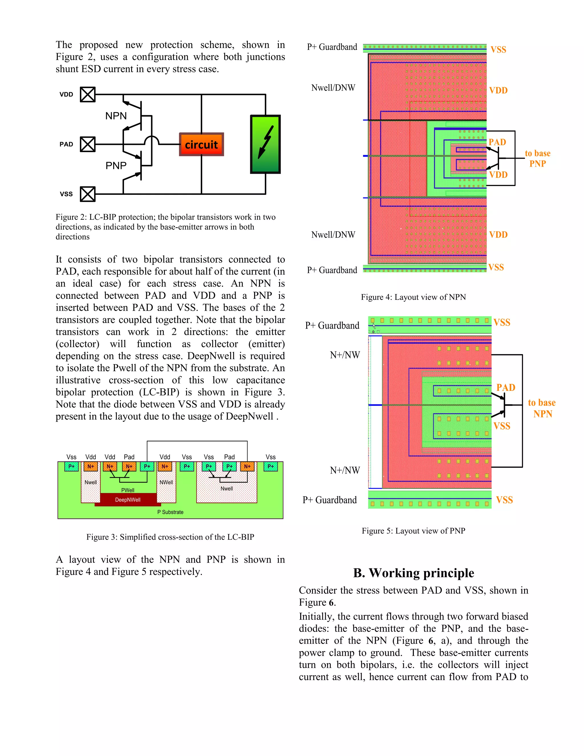
![that this is inherent in any diode string that contains a
parasitic Darlington chain, and therefore this is not
considered to be problematic.
C. Analysis of the improved low
capacitance bipolar protection
On a 28nm test chip different dual diode and LC-BIP
protection strategies have been tested. A power clamp
has been added to measure the different stress cases.
The power clamp chosen for all strategies was a 1.8V
DTSCR [6], and a 1.8V input monitor was placed in
parallel with the protection devices (Figure 9). The
gate monitors have a measured breakdown voltage of
about 10V-12V.
Figure 8: Working principle of the LC-BIP
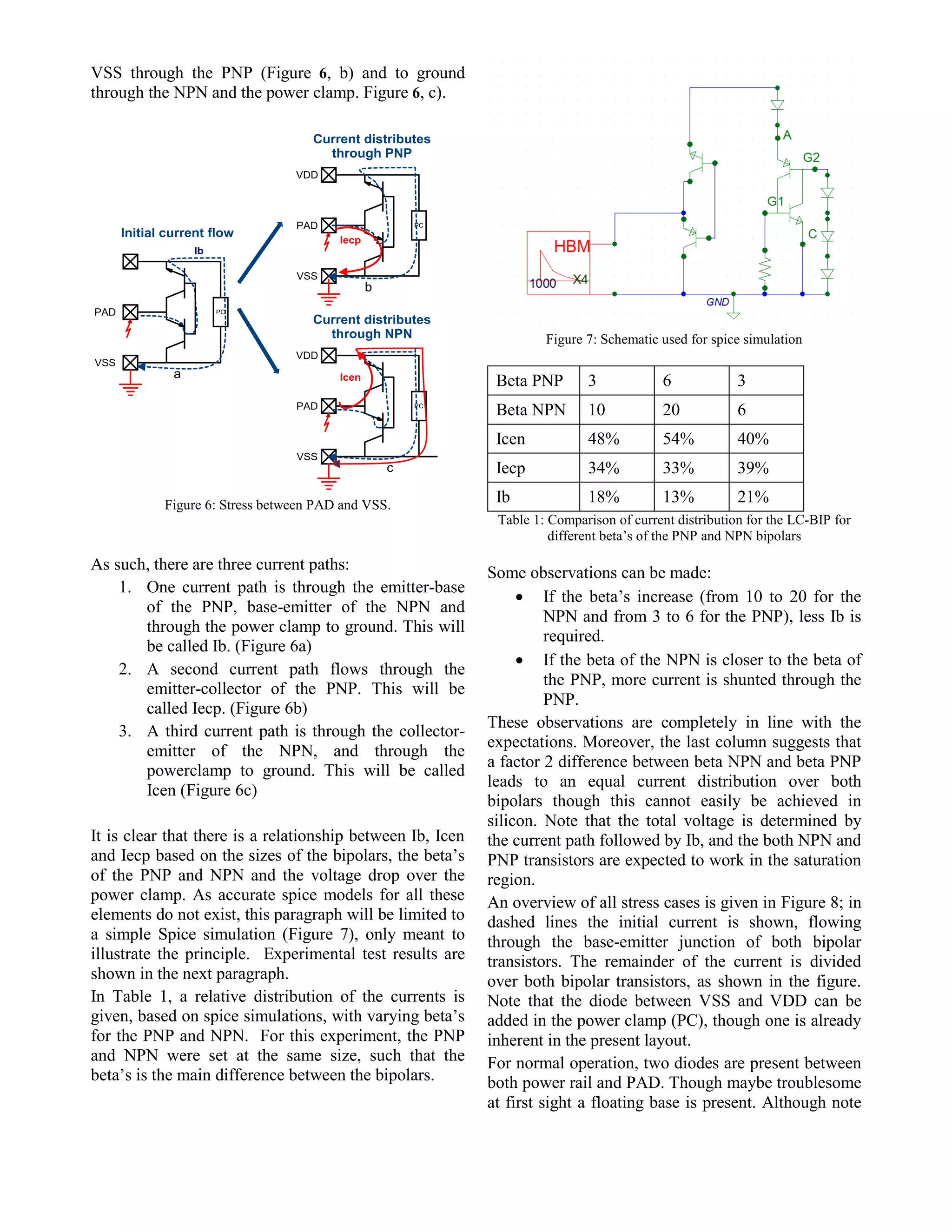
a: Stress between Pad and VSS
b: Stress between VDD and Pad
c: Stress between VSS and Pad
d: Stress between Pad and VDD
Figure 10 shows the TLP-IV curves of the dual diode
protection (DD), the double dual diode (DD2) and the
LC-BIP (with about 30% less junction area connected
to pad as compared to the dual diode) for the PAD to
VSS stress case. For completeness, the TLP result of
the power clamp itself is shown as well.
Figure 9: 1.8V test structure
The TLP curves also highlight the main drawback of
the LC-BIP concept: the resistance between PAD and
VSS is higher as compared to a classical dual diode.
This leads to a lower TLP failure current. For the DD2
approach the increase in on-resistance is even larger,
and subsequently, the It2 is even lower. However, the
correct figure of merit shall be the ratio of the TLP
current over the parasitic capacitance. The LC-BIP
shows a failure current of almost 1.2A for only 50fF.
0
0.25
0.5
0.75
1
1.25
1.5
1.75
2
0 5 10 15
10
-10
10
-9
10
-8
10
-7
10
-6
10
-5
10
-4
10
-3
10
-2
DD
LC-BIP
1.8V DTSCR
DD2
I [A]
V [V]
97fF
50fF
53fF
PAD to VSS
Figure 10: IV curves of different low capacitance protection
strategies (Leakage measured at 1.8V) for a positive stress
between PAD and VSS with a 1.8V gate monitor in parallel.
Figure 11 shows the TLP-IV curves of the low cap
protections for the VSS to PAD stress case. These
results show a lower on resistance for the LC-BIP
compared to the DD2 approach. Indeed, the bipolar
action creates a parallel current path, lowering the
resistance.](https://image.slidesharecdn.com/2017eosesd-201223162216/75/2017-Low-Capacitive-Dual-Bipolar-ESD-Protection-4-2048.jpg)
![0
0.5
1
1.5
2
0 2 4 6 8 10 12 14
10
-11
10
-9
10
-7
10
-5
10
-3
DD
DD2
LC-BIP
I [A]
V [V]
VSS to PAD
Figure 11: IV curves of different low capacitance protection
strategies (Leakage measured at 1.8V) for a positive stress
between VSS and PAD with a 1.8V gate monitor in parallel.
A large reduction of capacitance is achieved for the
same TLP performance [7], [8]. The capacitance
values shown are the SPICE simulated parasitic
junction capacitance values of the different strategies.
Table 2 shows the junction capacitance value per ESD
current (fF/A). The area, including P+ and Nwell
guard rings, is included in the table for completeness.
Concept Cap It2 Cap/It2 Area
DD 97fF 1.5A 64.7fF/A 310um²
DD2 53fF 0.9A 58.9fF/A 661um²
LC-BIP 50fF 1.2A 41.7fF/A 618um²
Table 2: Junction capacitance and It2 compared
Also, the parasitic junction capacitance of the LC-BIP
shows good linearity over a range of voltage levels
and for elevated temperatures.
Figure 12 shows the linearity of the parasitic junction
capacitance for a classical dual diode (DD) and for the
improved protection (LC-BIP) – for both 25°C and
85°C, and across a voltage sweep at the PAD from 0V
to 2.0V with a supply voltage of 1.8V. The junction
capacitance linearity for the improved low
capacitance bipolar protection is obvious as is the
insensitivity to temperature.
Figure 12: Junction capacitance linearity over a voltage range and
for elevated temperature
A VF-TLP analysis is done to evaluate the
performance during a CDM event. The rise-time is set
to 100ps, pulse width is set to 10ns. This is the most
severe pulse that can be supplied with the system. The
result is shown in Figure 13. From this plot, it can be
seen that the same conclusion can be drawn from the
VF-TLP data as compared to the regular TLP data: the
It2 of the LC-BIP is lower as compared to the dual
diode, but the fF/It2 is much better for the LC-BIP
(41.7fF/A vs 64.7fF/A).
0
0,2
0,4
0,6
0,8
1
1,2
1,4
0 2 4 6 8 10 12
10
-10
10
-9
10
-8
10
-7
10
-6
10
-5
10
-4
10
-3
10
-2
LC-BIP
DD
I[A]
V [V]
97fF
50fF
PAD to VSS
Figure 13: VF-TLP comparison of DD and LC-BIP results
(Leakage measured at 1.8V) for a positive stress between PAD
and VSS with a 1.8V gate monitor in parallel.
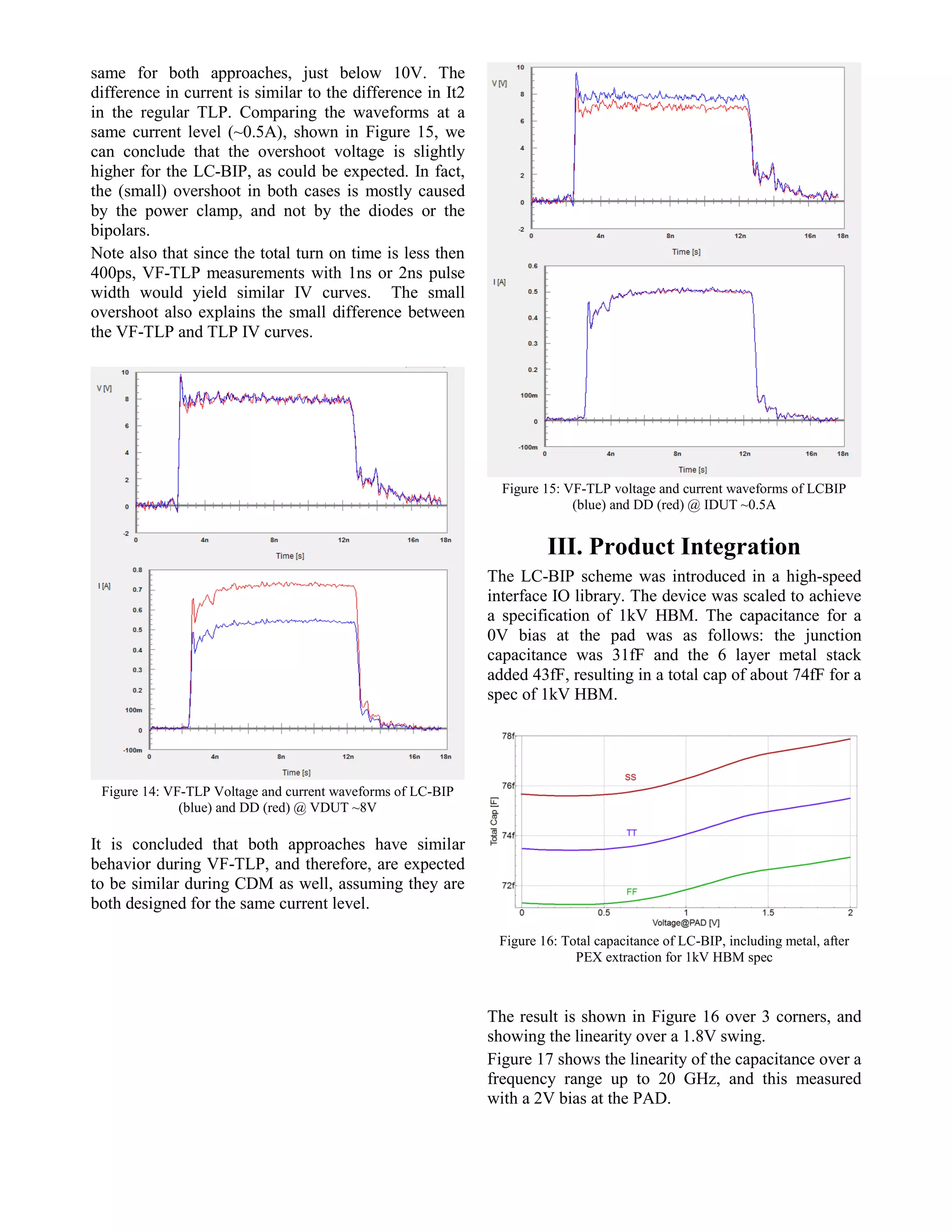
As the It2 of the VF-TLP measurement is slightly
lower than the It2 of the TLP measurement, the
waveforms are studied to investigate the overshoot.
Comparison with dual diode is non-trivial, as the LC-
BIP has higher on-resistance, and therefore the
voltage is higher for the same current level.
Based on the waveforms taken from the LC-BIP and
DD at a same voltage level (~8V), shown in Figure
14, it can be seen that the overshoot voltage is the](https://image.slidesharecdn.com/2017eosesd-201223162216/75/2017-Low-Capacitive-Dual-Bipolar-ESD-Protection-5-2048.jpg)
![Figure 17: Total Capacitance of LC-BIP @ 2V over a frequency
range of 20GHz
Based on VF-TLP analysis no intrinsic CDM issues
with this IO are expected. Figure 18 shows similar
PEX extraction with dual diode designed for 1kV
HBM.
Figure 18: Total Capacitance of DD, including metal, after PEX
extraction for 1kV HBM spec
E. Further optimizations
Further optimization of the approach is possible.
A first possible optimization is to study the bipolar
devices for optimal layout. The number of contact
rows for instance has influence on the junction
capacitance for sure, but possibly also on the current
capability and (more importantly) on resistance.
A second optimization consists of finding the ideal
balance between NPN and PNP bipolar. As is well
known, it can be expected that the NPN has a higher
beta, and therefore the area can potentially be smaller
as compared to the PNP. The ideal balance should
take into account all four stress combinations.
As shown, the current LC-BIP solution has about
double the size of the dual diode approach. Though
this was not a concern for the given application,
further work can be done to optimize the balance
between NPN and PNP over all stress cases to
minimize total area.
Furthermore, it will be studied if the approach can be
ported to the LV domain, by lowering the total
resistance.
Conclusions
A new protection concept [9] is introduced in which
the utilization of the junctions connected to PAD
during ESD is optimized to lower the junction
capacitance. TLP and VF-TLP measurements
highlight the ESD capabilities.
References
[1] M.K. Radhakrishnan et al., “ESD Reliablity Issues
in RF CMOS Circuits”, 2001
[2] Feng K et al., “A comparison study of ESD
protection for RFICs: performance versus
parasitic”, 2000 IEEE RFI
[3] R.M.D.A Velghe et al, “Diode Network Used as
ESD Protection in RF Applications”, EOS/ESD
Symposium, 2001
[4] K. Bhatia et al., “Layout Guidelines for
Optimized ESD Protection Diodes”, EOS/ESD
Symposium, 2007
[5] G. Boselli et al., “Analysis of ESD Protection
Components in 65nm CMOS: Scaling Perspective
and Impact on ESD Design Window, EOS/ESD
Symposium, 2005
[6] M. Mergens et al, “Diode-Triggered SCR
(DTSCR) for RF-ESD Protection of BiCMOS
SiGe HBTs and CMOS Ultra-Thin Gate Oxides”,
IEDM 2003
[7] E. R. Worley et al., “Optimization of Input
Protection Diode for High Speed Applications”,
EOS/ESD Symposium, 2002
[8] S. Hyvonen et al., “Diode-Based Tuned ESD
Protection for 5.25-GHz CMOS LNAs”,
EOS/ESD Symposium, 2005
[9] US 8,283,698 Electrostatic Discharge Protection](https://image.slidesharecdn.com/2017eosesd-201223162216/75/2017-Low-Capacitive-Dual-Bipolar-ESD-Protection-7-2048.jpg)


