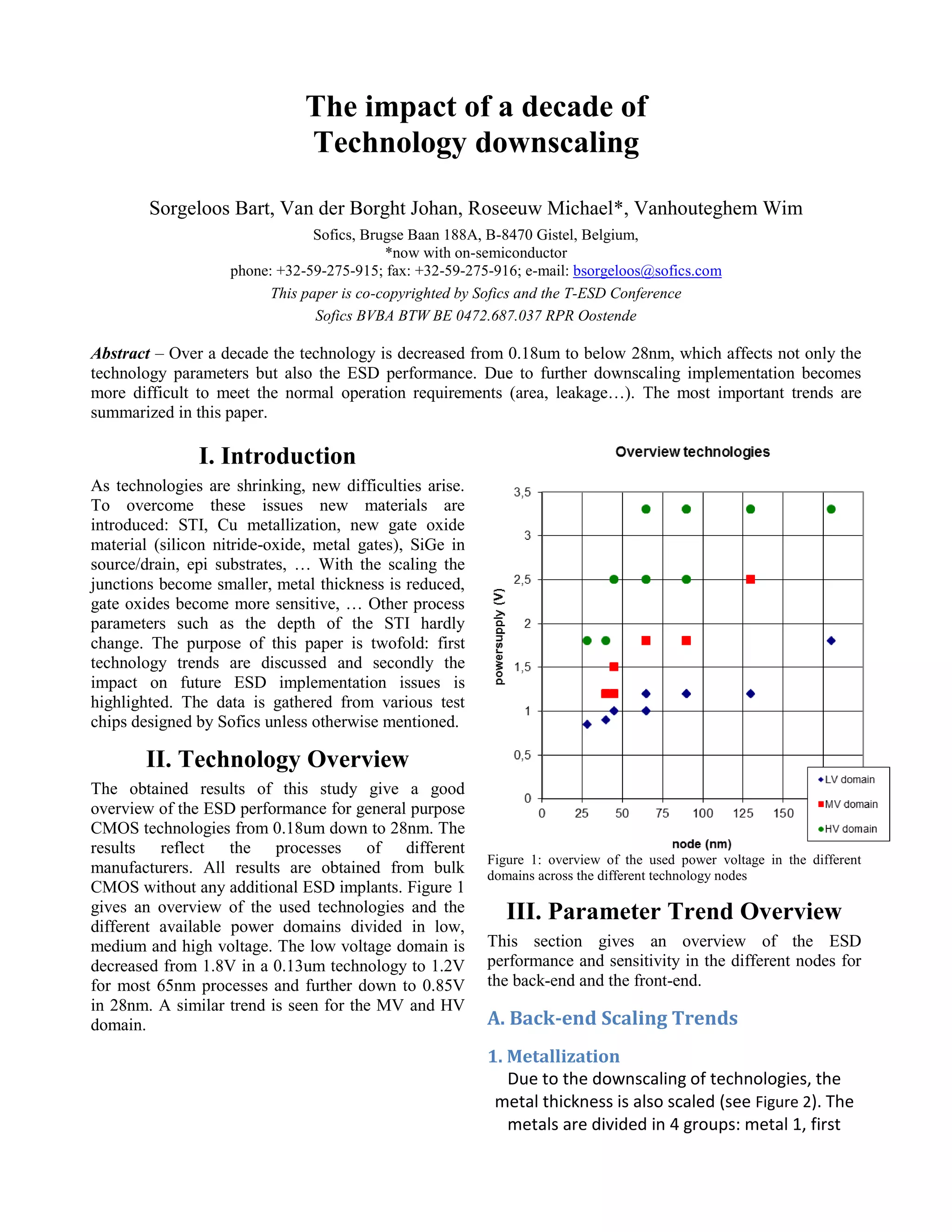
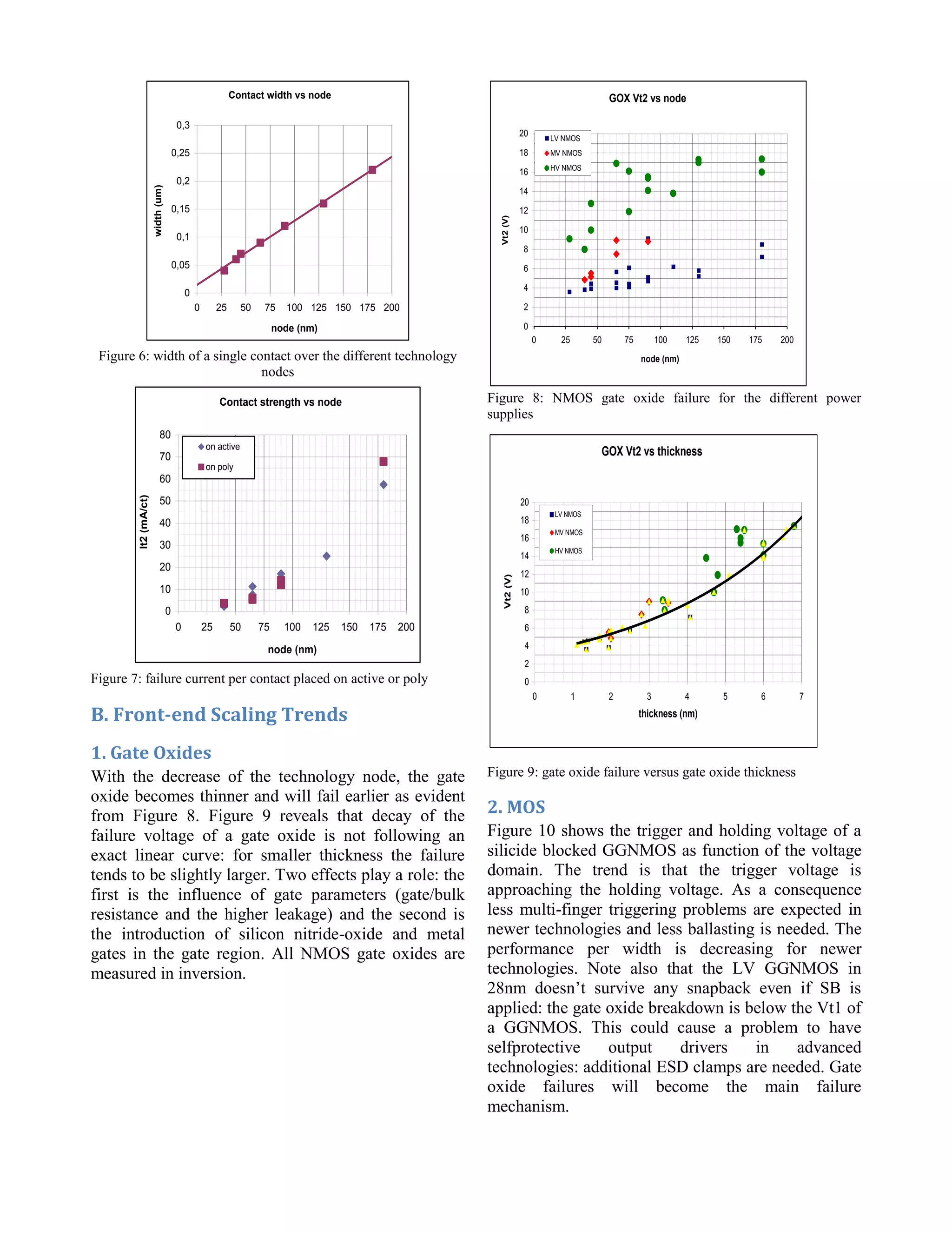
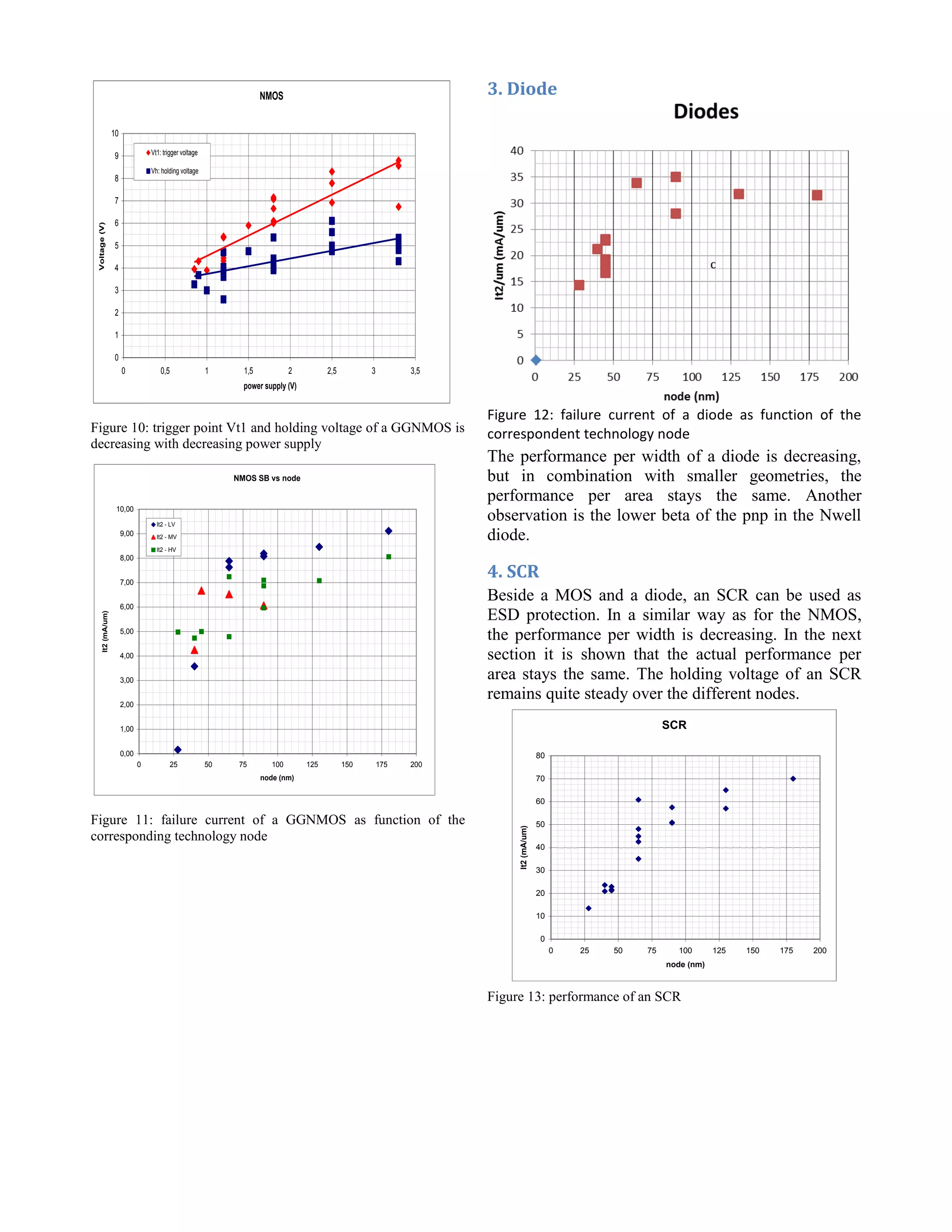
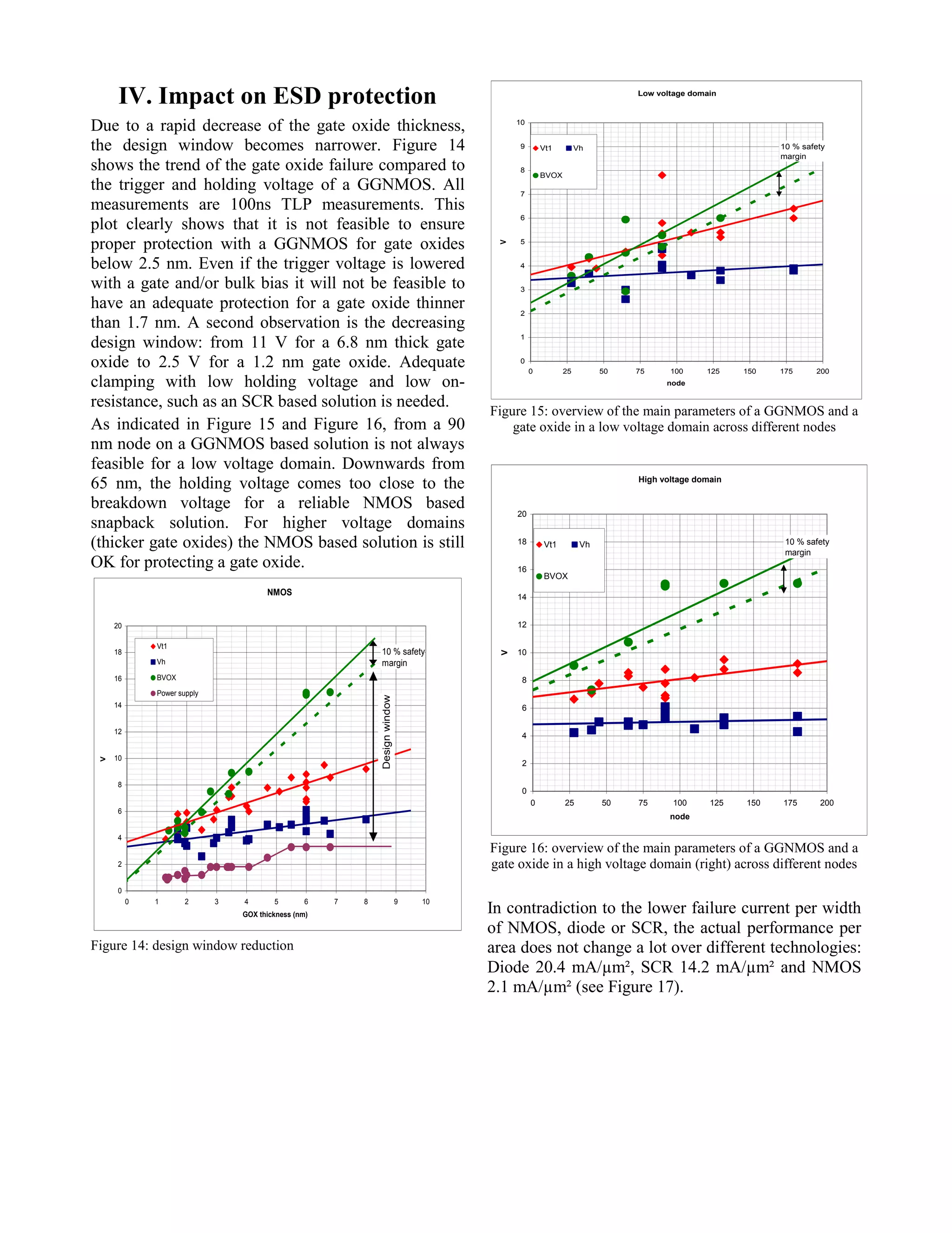
Conference paper The impact of a decade of Technology
downscaling
Taiwan ESD and reliability conference 2012
Over a decade the technology is decreased from 0.18um to below
28nm, which affects not only the technology parameters but also the
ESD performance. Due to further downscaling implementation
becomes more difficult to meet the normal operation requirements
(area, leakage…). The most important trends are summarized in this
paper.
The impact of a decade of
Technology downscaling
Sorgeloos Bart, Van der Borght Johan, Roseeuw Michael*, Vanhouteghem Wim
Sofics, Brugse Baan 188A, B-8470 Gistel, Belgium,
*now with on-semiconductor
phone: +32-59-275-915; fax: +32-59-275-916; e-mail: bsorgeloos@sofics.com
This paper is co-copyrighted by Sofics and the T-ESD Conference
Sofics BVBA BTW BE 0472.687.037 RPR Oostende
Abstract – Over a decade the technology is decreased from 0.18um to below 28nm, which affects not only the
technology parameters but also the ESD performance. Due to further downscaling implementation becomes
more difficult to meet the normal operation requirements (area, leakage…). The most important trends are
summarized in this paper.
I. Introduction
As technologies are shrinking, new difficulties arise.
To overcome these issues new materials are
introduced: STI, Cu metallization, new gate oxide
material (silicon nitride-oxide, metal gates), SiGe in
source/drain, epi substrates, … With the scaling the
junctions become smaller, metal thickness is reduced,
gate oxides become more sensitive, … Other process
parameters such as the depth of the STI hardly
change. The purpose of this paper is twofold: first
technology trends are discussed and secondly the
impact on future ESD implementation issues is
highlighted. The data is gathered from various test
chips designed by Sofics unless otherwise mentioned.
II. Technology Overview
The obtained results of this study give a good
overview of the ESD performance for general purpose
CMOS technologies from 0.18um down to 28nm. The
results reflect the processes of different
manufacturers. All results are obtained from bulk
CMOS without any additional ESD implants. Figure 1
gives an overview of the used technologies and the
different available power domains divided in low,
medium and high voltage. The low voltage domain is
decreased from 1.8V in a 0.13um technology to 1.2V
for most 65nm processes and further down to 0.85V
in 28nm. A similar trend is seen for the MV and HV
domain.
Figure 1: overview of the used power voltage in the different
domains across the different technology nodes
III. Parameter Trend Overview
This section gives an overview of the ESD
performance and sensitivity in the different nodes for
the back-end and the front-end.
A. Back-end Scaling Trends
1. Metallization
Due to the downscaling of technologies, the
metal thickness is also scaled (see Figure 2). The
metals are divided in 4 groups: metal 1, first
intermediate metal (mostly used for the local
connections), the second intermediate metal
(used for busses) and global metal. One of the
difficulties in 65nm and below is that not only
the lowest metals decrease in thickness, but also
the second intermediate metals become a lot
thinner: a decrease in thickness of more than 4
times from 0.18um to 28nm. This thickness
reduction results in a lower ESD performance
correlating with the thickness (see
Figure 3). All metals are Cu based, except for 0.18um
(AlCu).
Figure 3 shows the linear scaling of the metal
strength/µm thickness. Besides the lower ESD
performance an increase in the resistance is observed.
This will impact the maximum distance from a
sensitive node to an ESD clamp. Since the ESD
current stays the same and the design window
decreases it becomes more and more difficult to
provide adequate metallization.
Thickness vs node
0
200
400
600
800
1000
1200
0 25 50 75 100 125 150 175 200
node (nm)
thickness(nm)
First metal
First intermediate metal
Second intermediate metal
Global metal
Linear (Global metal)
Figure 2: decreasing metal thickness across the technology nodes
Metal strength vs thickness
0
100
200
300
400
500
600
700
800
900
1000
1100
0 200 400 600 800 1000
Thickness (nm)
It2(mA/um)
First metal
First intermediate metal
Second intermediate metal
Global metal
Figure 3: linear scaling of the failure current of metal according
the thickness
2. Contact/Vias
A similar effect as for the metals is observed for the
vias: due to scaling of the front end, the via size and
strength is decreasing with newer technologies. The
failure current in Figure 5 is measured for an array of
4 by 5 vias in all the technologies. A decrease from
175 to below 30 mA/via is seen over the technologies.
This decrease (factor 11) is larger than the reduction
of the size (factor 7) due to more local heating (less
space between the vias). One effect that is not taken
in consideration in this data is that the density of vias
is increased for the same area. The overall
performance per area stays nearly the same across the
different technologies. This means that the area that is
needed for ESD protection does not decrease over the
different technologies.
Via width vs node
0
0,1
0,2
0,3
0,4
0,5
0,6
0,7
0 25 50 75 100 125 150 175 200
node (nm)
width(um)
first via
first intermediate via
second intermediate via
global via
Figure 4: width of a single via over the different technology nodes
Via strength vs width
0
100
200
300
400
500
600
700
800
900
0 0,1 0,2 0,3 0,4 0,5 0,6 0,7
width (um)
It2(mA/um)
first intermediate via
second intermediate via
global via
Figure 5: failure current per via width
Figure 6 and Figure 7 show the results for one contact
in the same configuration. Similar conclusions as for
the vias are valid.
Contact width vs node
0
0,05
0,1
0,15
0,2
0,25
0,3
0 25 50 75 100 125 150 175 200
node (nm)
width(um)
Figure 6: width of a single contact over the different technology
nodes
Contact strength vs node
0
10
20
30
40
50
60
70
80
0 25 50 75 100 125 150 175 200
node (nm)
It2(mA/ct)
on active
on poly
Figure 7: failure current per contact placed on active or poly
B. Front-end Scaling Trends
1. Gate Oxides
With the decrease of the technology node, the gate
oxide becomes thinner and will fail earlier as evident
from Figure 8. Figure 9 reveals that decay of the
failure voltage of a gate oxide is not following an
exact linear curve: for smaller thickness the failure
tends to be slightly larger. Two effects play a role: the
first is the influence of gate parameters (gate/bulk
resistance and the higher leakage) and the second is
the introduction of silicon nitride-oxide and metal
gates in the gate region. All NMOS gate oxides are
measured in inversion.
GOX Vt2 vs node
0
2
4
6
8
10
12
14
16
18
20
0 25 50 75 100 125 150 175 200
node (nm)
Vt2(V)
LV NMOS
MV NMOS
HV NMOS
Figure 8: NMOS gate oxide failure for the different power
supplies
GOX Vt2 vs thickness
0
2
4
6
8
10
12
14
16
18
20
0 1 2 3 4 5 6 7
thickness (nm)
Vt2(V)
LV NMOS
MV NMOS
HV NMOS
Figure 9: gate oxide failure versus gate oxide thickness
2. MOS
Figure 10 shows the trigger and holding voltage of a
silicide blocked GGNMOS as function of the voltage
domain. The trend is that the trigger voltage is
approaching the holding voltage. As a consequence
less multi-finger triggering problems are expected in
newer technologies and less ballasting is needed. The
performance per width is decreasing for newer
technologies. Note also that the LV GGNMOS in
28nm doesn’t survive any snapback even if SB is
applied: the gate oxide breakdown is below the Vt1 of
a GGNMOS. This could cause a problem to have
selfprotective output drivers in advanced
technologies: additional ESD clamps are needed. Gate
oxide failures will become the main failure
mechanism.
NMOS
0
1
2
3
4
5
6
7
8
9
10
0 0,5 1 1,5 2 2,5 3 3,5
power supply (V)
Voltage(V)
Vt1: trigger voltage
Vh: holding voltage
Figure 10: trigger point Vt1 and holding voltage of a GGNMOS is
decreasing with decreasing power supply
NMOS SB vs node
0,00
1,00
2,00
3,00
4,00
5,00
6,00
7,00
8,00
9,00
10,00
0 25 50 75 100 125 150 175 200
node (nm)
It2(mA/um)
It2 - LV
It2 - MV
It2 - HV
Figure 11: failure current of a GGNMOS as function of the
corresponding technology node
3. Diode
Figure 12: failure current of a diode as function of the
correspondent technology node
The performance per width of a diode is decreasing,
but in combination with smaller geometries, the
performance per area stays the same. Another
observation is the lower beta of the pnp in the Nwell
diode.
4. SCR
Beside a MOS and a diode, an SCR can be used as
ESD protection. In a similar way as for the NMOS,
the performance per width is decreasing. In the next
section it is shown that the actual performance per
area stays the same. The holding voltage of an SCR
remains quite steady over the different nodes.
SCR
0
10
20
30
40
50
60
70
80
0 25 50 75 100 125 150 175 200
node (nm)
It2(mA/um)
Figure 13: performance of an SCR
IV. Impact on ESD protection
Due to a rapid decrease of the gate oxide thickness,
the design window becomes narrower. Figure 14
shows the trend of the gate oxide failure compared to
the trigger and holding voltage of a GGNMOS. All
measurements are 100ns TLP measurements. This
plot clearly shows that it is not feasible to ensure
proper protection with a GGNMOS for gate oxides
below 2.5 nm. Even if the trigger voltage is lowered
with a gate and/or bulk bias it will not be feasible to
have an adequate protection for a gate oxide thinner
than 1.7 nm. A second observation is the decreasing
design window: from 11 V for a 6.8 nm thick gate
oxide to 2.5 V for a 1.2 nm gate oxide. Adequate
clamping with low holding voltage and low on-
resistance, such as an SCR based solution is needed.
As indicated in Figure 15 and Figure 16, from a 90
nm node on a GGNMOS based solution is not always
feasible for a low voltage domain. Downwards from
65 nm, the holding voltage comes too close to the
breakdown voltage for a reliable NMOS based
snapback solution. For higher voltage domains
(thicker gate oxides) the NMOS based solution is still
OK for protecting a gate oxide.
NMOS
0
2
4
6
8
10
12
14
16
18
20
0 1 2 3 4 5 6 7 8 9 10
GOX thickness (nm)
V
Vt1
Vh
BVOX
Power supply
10 % safety
margin
Designwindow
Figure 14: design window reduction
Low voltage domain
0
1
2
3
4
5
6
7
8
9
10
0 25 50 75 100 125 150 175 200
node
V
Vt1 Vh
BVOX
10 % safety
margin
Figure 15: overview of the main parameters of a GGNMOS and a
gate oxide in a low voltage domain across different nodes
High voltage domain
0
2
4
6
8
10
12
14
16
18
20
0 25 50 75 100 125 150 175 200
node
V
Vt1 Vh
BVOX
10 % safety
margin
Figure 16: overview of the main parameters of a GGNMOS and a
gate oxide in a high voltage domain (right) across different nodes
In contradiction to the lower failure current per width
of NMOS, diode or SCR, the actual performance per
area does not change a lot over different technologies:
Diode 20.4 mA/µm², SCR 14.2 mA/µm² and NMOS
2.1 mA/µm² (see Figure 17).
Overview
0
5
10
15
20
25
0 20 40 60 80 100 120
node (nm)
It2/um²
It2 - NMOS
It2 - diode
It2 - SCR
Figure 17: ESD performance/area
As shown on Figure 17, the performance per area
remains constant for basic devices like diodes and
SCRs. The following two plots (Figures 18 and 19)
show that this can strongly simplify the transfer of
ESD solutions between technology nodes and
fabrication plants if the appropriate ESD concepts are
used. Figure 18 shows measurements on proprietary
DTSCR (diode triggered SCR) clamps for low voltage
protection on 4 different generations (180nm, 130nm,
65nm and 40nm).It is obvious that the trigger and
clamping behavior is identical for all devices. The
current axis in the plot is normalized to compare
devices with different device width.
Figure 18: DT-SCR devices for thin oxide interface protection
measured on TSMC technology between 180nm and 40nm. The
triggering and clamping behavior is identical across technology
nodes.
On Figure 19, DTSCR devices for 3.3V protection in
40nm and 28nm are compared. The behavior is
identical.
0
0.5
1
1.5
2
2.5
3
3.5
4
0 5 10 15
10
-11
10
-9
10
-7
10
-5
0.001
3V PowerClamp: 28nm vs 40nm
28nm (3V)
28nm (3.3V)
40nm (3.3V)
IDUT(Amps)
V DUT(Volts)
I LEAKAGE(Amps)
Figure 19: 3.3V DTSCR power clamp devices measured on 40nm
and 28nm technology. The clamps have an identical behavior.
Conclusion
Due to technology scaling a GGNMOS is not feasible
anymore as standalone ESD protection device in
advanced processes. Although the devices are strongly
reduced in size, the actual ESD performance per area
doesn’t change. This means ESD protection area does
not scale down with the technology node. Another
challenge for these newer technologies is to overcome
the lower performance per area of the metal (thinner
metal). This makes that very often the metallization
becomes the bottleneck. The ESD capability is OK
but the implementation can be more complex in
advanced processes.
References
[1] Christian Russ et al., “ESD issues in advanced CMOS
bulk and FinFET technologies: Processing,protection
devices and circuit strategies”, Microelectronics
Reliability 48, 2008
[2] Steven H. Voldman, “A review of electrostatic
discharge (ESD) in advanced semiconductor
technology”, Microelectronics Reliability 44, 2004
[3] Gianluca Boselli et al., “Analysis of ESD Protection
Components in 65nm CMOS Technology: Scaling
Perspective and Impact on ESD Design Window”,
EOS/ESD 2005
[4] Markus Mergens et al., “Speed optimized diode-
triggered SCR (DTSCR) for RF-ESD protection of
ultra-sensitive IC nodes in advanced technologies”,
IEEE Trans Dev Mater Reliab 2005;5
0 1 2 3
180nm
130nm
65nm
40nm
I [A.U.]
V [V]
Sofics Proprietary – ©2012
About Sofics
Sofics (www.sofics.com) is the world leader in on-chip ESD protection. Its
patented technology is proven in more than a thousand IC designs across all
major foundries and process nodes. IC companies of all sizes rely on Sofics for off-
the-shelf or custom-crafted solutions to protect overvoltage I/Os, other non-
standard I/Os, and high-voltage ICs, including those that require system-level
protection on the chip. Sofics technology produces smaller I/Os than any generic
ESD configuration. It also permits twice the IC performance in high-frequency and
high-speed applications. Sofics ESD solutions and service begin where the foundry
design manual ends.
Our service and support
Our business models include
 Single-use, multi-use or royalty bearing license for ESD clamps
 Services to customize ESD protection
o Enable unique requirements for Latch-up, ESD, EOS
o Layout, metallization and aspect ratio customization
o Area, capacitance, leakage optimization
 Transfer of individual clamps to another target technology
 Develop custom ESD clamps for foundry or proprietary process
 Debugging and correcting an existing IC or IO
 ESD testing and analysis
Notes
As is the case with many published ESD design solutions, the techniques and
protection solutions described in this data sheet are protected by patents and
patents pending and cannot be copied freely. PowerQubic, TakeCharge, and
Sofics are trademarks of Sofics BVBA.
Version
December 2012
ESD SOLUTIONS AT YOUR FINGERTIPS
Sofics BVBA
Groendreef 31
B-9880 Aalter, Belgium
(tel) +32-9-21-68-333
(fax) +32-9-37-46-846
bd@sofics.com
RPR 0472.687.037

2012 The impact of a decade of Technology downscaling

  • 1.
    Conference paper Theimpact of a decade of Technology downscaling Taiwan ESD and reliability conference 2012 Over a decade the technology is decreased from 0.18um to below 28nm, which affects not only the technology parameters but also the ESD performance. Due to further downscaling implementation becomes more difficult to meet the normal operation requirements (area, leakage…). The most important trends are summarized in this paper.
  • 2.
    The impact ofa decade of Technology downscaling Sorgeloos Bart, Van der Borght Johan, Roseeuw Michael*, Vanhouteghem Wim Sofics, Brugse Baan 188A, B-8470 Gistel, Belgium, *now with on-semiconductor phone: +32-59-275-915; fax: +32-59-275-916; e-mail: bsorgeloos@sofics.com This paper is co-copyrighted by Sofics and the T-ESD Conference Sofics BVBA BTW BE 0472.687.037 RPR Oostende Abstract – Over a decade the technology is decreased from 0.18um to below 28nm, which affects not only the technology parameters but also the ESD performance. Due to further downscaling implementation becomes more difficult to meet the normal operation requirements (area, leakage…). The most important trends are summarized in this paper. I. Introduction As technologies are shrinking, new difficulties arise. To overcome these issues new materials are introduced: STI, Cu metallization, new gate oxide material (silicon nitride-oxide, metal gates), SiGe in source/drain, epi substrates, … With the scaling the junctions become smaller, metal thickness is reduced, gate oxides become more sensitive, … Other process parameters such as the depth of the STI hardly change. The purpose of this paper is twofold: first technology trends are discussed and secondly the impact on future ESD implementation issues is highlighted. The data is gathered from various test chips designed by Sofics unless otherwise mentioned. II. Technology Overview The obtained results of this study give a good overview of the ESD performance for general purpose CMOS technologies from 0.18um down to 28nm. The results reflect the processes of different manufacturers. All results are obtained from bulk CMOS without any additional ESD implants. Figure 1 gives an overview of the used technologies and the different available power domains divided in low, medium and high voltage. The low voltage domain is decreased from 1.8V in a 0.13um technology to 1.2V for most 65nm processes and further down to 0.85V in 28nm. A similar trend is seen for the MV and HV domain. Figure 1: overview of the used power voltage in the different domains across the different technology nodes III. Parameter Trend Overview This section gives an overview of the ESD performance and sensitivity in the different nodes for the back-end and the front-end. A. Back-end Scaling Trends 1. Metallization Due to the downscaling of technologies, the metal thickness is also scaled (see Figure 2). The metals are divided in 4 groups: metal 1, first
  • 3.
    intermediate metal (mostlyused for the local connections), the second intermediate metal (used for busses) and global metal. One of the difficulties in 65nm and below is that not only the lowest metals decrease in thickness, but also the second intermediate metals become a lot thinner: a decrease in thickness of more than 4 times from 0.18um to 28nm. This thickness reduction results in a lower ESD performance correlating with the thickness (see Figure 3). All metals are Cu based, except for 0.18um (AlCu). Figure 3 shows the linear scaling of the metal strength/µm thickness. Besides the lower ESD performance an increase in the resistance is observed. This will impact the maximum distance from a sensitive node to an ESD clamp. Since the ESD current stays the same and the design window decreases it becomes more and more difficult to provide adequate metallization. Thickness vs node 0 200 400 600 800 1000 1200 0 25 50 75 100 125 150 175 200 node (nm) thickness(nm) First metal First intermediate metal Second intermediate metal Global metal Linear (Global metal) Figure 2: decreasing metal thickness across the technology nodes Metal strength vs thickness 0 100 200 300 400 500 600 700 800 900 1000 1100 0 200 400 600 800 1000 Thickness (nm) It2(mA/um) First metal First intermediate metal Second intermediate metal Global metal Figure 3: linear scaling of the failure current of metal according the thickness 2. Contact/Vias A similar effect as for the metals is observed for the vias: due to scaling of the front end, the via size and strength is decreasing with newer technologies. The failure current in Figure 5 is measured for an array of 4 by 5 vias in all the technologies. A decrease from 175 to below 30 mA/via is seen over the technologies. This decrease (factor 11) is larger than the reduction of the size (factor 7) due to more local heating (less space between the vias). One effect that is not taken in consideration in this data is that the density of vias is increased for the same area. The overall performance per area stays nearly the same across the different technologies. This means that the area that is needed for ESD protection does not decrease over the different technologies. Via width vs node 0 0,1 0,2 0,3 0,4 0,5 0,6 0,7 0 25 50 75 100 125 150 175 200 node (nm) width(um) first via first intermediate via second intermediate via global via Figure 4: width of a single via over the different technology nodes Via strength vs width 0 100 200 300 400 500 600 700 800 900 0 0,1 0,2 0,3 0,4 0,5 0,6 0,7 width (um) It2(mA/um) first intermediate via second intermediate via global via Figure 5: failure current per via width Figure 6 and Figure 7 show the results for one contact in the same configuration. Similar conclusions as for the vias are valid.
  • 4.
    Contact width vsnode 0 0,05 0,1 0,15 0,2 0,25 0,3 0 25 50 75 100 125 150 175 200 node (nm) width(um) Figure 6: width of a single contact over the different technology nodes Contact strength vs node 0 10 20 30 40 50 60 70 80 0 25 50 75 100 125 150 175 200 node (nm) It2(mA/ct) on active on poly Figure 7: failure current per contact placed on active or poly B. Front-end Scaling Trends 1. Gate Oxides With the decrease of the technology node, the gate oxide becomes thinner and will fail earlier as evident from Figure 8. Figure 9 reveals that decay of the failure voltage of a gate oxide is not following an exact linear curve: for smaller thickness the failure tends to be slightly larger. Two effects play a role: the first is the influence of gate parameters (gate/bulk resistance and the higher leakage) and the second is the introduction of silicon nitride-oxide and metal gates in the gate region. All NMOS gate oxides are measured in inversion. GOX Vt2 vs node 0 2 4 6 8 10 12 14 16 18 20 0 25 50 75 100 125 150 175 200 node (nm) Vt2(V) LV NMOS MV NMOS HV NMOS Figure 8: NMOS gate oxide failure for the different power supplies GOX Vt2 vs thickness 0 2 4 6 8 10 12 14 16 18 20 0 1 2 3 4 5 6 7 thickness (nm) Vt2(V) LV NMOS MV NMOS HV NMOS Figure 9: gate oxide failure versus gate oxide thickness 2. MOS Figure 10 shows the trigger and holding voltage of a silicide blocked GGNMOS as function of the voltage domain. The trend is that the trigger voltage is approaching the holding voltage. As a consequence less multi-finger triggering problems are expected in newer technologies and less ballasting is needed. The performance per width is decreasing for newer technologies. Note also that the LV GGNMOS in 28nm doesn’t survive any snapback even if SB is applied: the gate oxide breakdown is below the Vt1 of a GGNMOS. This could cause a problem to have selfprotective output drivers in advanced technologies: additional ESD clamps are needed. Gate oxide failures will become the main failure mechanism.
  • 5.
    NMOS 0 1 2 3 4 5 6 7 8 9 10 0 0,5 11,5 2 2,5 3 3,5 power supply (V) Voltage(V) Vt1: trigger voltage Vh: holding voltage Figure 10: trigger point Vt1 and holding voltage of a GGNMOS is decreasing with decreasing power supply NMOS SB vs node 0,00 1,00 2,00 3,00 4,00 5,00 6,00 7,00 8,00 9,00 10,00 0 25 50 75 100 125 150 175 200 node (nm) It2(mA/um) It2 - LV It2 - MV It2 - HV Figure 11: failure current of a GGNMOS as function of the corresponding technology node 3. Diode Figure 12: failure current of a diode as function of the correspondent technology node The performance per width of a diode is decreasing, but in combination with smaller geometries, the performance per area stays the same. Another observation is the lower beta of the pnp in the Nwell diode. 4. SCR Beside a MOS and a diode, an SCR can be used as ESD protection. In a similar way as for the NMOS, the performance per width is decreasing. In the next section it is shown that the actual performance per area stays the same. The holding voltage of an SCR remains quite steady over the different nodes. SCR 0 10 20 30 40 50 60 70 80 0 25 50 75 100 125 150 175 200 node (nm) It2(mA/um) Figure 13: performance of an SCR
  • 6.
    IV. Impact onESD protection Due to a rapid decrease of the gate oxide thickness, the design window becomes narrower. Figure 14 shows the trend of the gate oxide failure compared to the trigger and holding voltage of a GGNMOS. All measurements are 100ns TLP measurements. This plot clearly shows that it is not feasible to ensure proper protection with a GGNMOS for gate oxides below 2.5 nm. Even if the trigger voltage is lowered with a gate and/or bulk bias it will not be feasible to have an adequate protection for a gate oxide thinner than 1.7 nm. A second observation is the decreasing design window: from 11 V for a 6.8 nm thick gate oxide to 2.5 V for a 1.2 nm gate oxide. Adequate clamping with low holding voltage and low on- resistance, such as an SCR based solution is needed. As indicated in Figure 15 and Figure 16, from a 90 nm node on a GGNMOS based solution is not always feasible for a low voltage domain. Downwards from 65 nm, the holding voltage comes too close to the breakdown voltage for a reliable NMOS based snapback solution. For higher voltage domains (thicker gate oxides) the NMOS based solution is still OK for protecting a gate oxide. NMOS 0 2 4 6 8 10 12 14 16 18 20 0 1 2 3 4 5 6 7 8 9 10 GOX thickness (nm) V Vt1 Vh BVOX Power supply 10 % safety margin Designwindow Figure 14: design window reduction Low voltage domain 0 1 2 3 4 5 6 7 8 9 10 0 25 50 75 100 125 150 175 200 node V Vt1 Vh BVOX 10 % safety margin Figure 15: overview of the main parameters of a GGNMOS and a gate oxide in a low voltage domain across different nodes High voltage domain 0 2 4 6 8 10 12 14 16 18 20 0 25 50 75 100 125 150 175 200 node V Vt1 Vh BVOX 10 % safety margin Figure 16: overview of the main parameters of a GGNMOS and a gate oxide in a high voltage domain (right) across different nodes In contradiction to the lower failure current per width of NMOS, diode or SCR, the actual performance per area does not change a lot over different technologies: Diode 20.4 mA/µm², SCR 14.2 mA/µm² and NMOS 2.1 mA/µm² (see Figure 17).
  • 7.
    Overview 0 5 10 15 20 25 0 20 4060 80 100 120 node (nm) It2/um² It2 - NMOS It2 - diode It2 - SCR Figure 17: ESD performance/area As shown on Figure 17, the performance per area remains constant for basic devices like diodes and SCRs. The following two plots (Figures 18 and 19) show that this can strongly simplify the transfer of ESD solutions between technology nodes and fabrication plants if the appropriate ESD concepts are used. Figure 18 shows measurements on proprietary DTSCR (diode triggered SCR) clamps for low voltage protection on 4 different generations (180nm, 130nm, 65nm and 40nm).It is obvious that the trigger and clamping behavior is identical for all devices. The current axis in the plot is normalized to compare devices with different device width. Figure 18: DT-SCR devices for thin oxide interface protection measured on TSMC technology between 180nm and 40nm. The triggering and clamping behavior is identical across technology nodes. On Figure 19, DTSCR devices for 3.3V protection in 40nm and 28nm are compared. The behavior is identical. 0 0.5 1 1.5 2 2.5 3 3.5 4 0 5 10 15 10 -11 10 -9 10 -7 10 -5 0.001 3V PowerClamp: 28nm vs 40nm 28nm (3V) 28nm (3.3V) 40nm (3.3V) IDUT(Amps) V DUT(Volts) I LEAKAGE(Amps) Figure 19: 3.3V DTSCR power clamp devices measured on 40nm and 28nm technology. The clamps have an identical behavior. Conclusion Due to technology scaling a GGNMOS is not feasible anymore as standalone ESD protection device in advanced processes. Although the devices are strongly reduced in size, the actual ESD performance per area doesn’t change. This means ESD protection area does not scale down with the technology node. Another challenge for these newer technologies is to overcome the lower performance per area of the metal (thinner metal). This makes that very often the metallization becomes the bottleneck. The ESD capability is OK but the implementation can be more complex in advanced processes. References [1] Christian Russ et al., “ESD issues in advanced CMOS bulk and FinFET technologies: Processing,protection devices and circuit strategies”, Microelectronics Reliability 48, 2008 [2] Steven H. Voldman, “A review of electrostatic discharge (ESD) in advanced semiconductor technology”, Microelectronics Reliability 44, 2004 [3] Gianluca Boselli et al., “Analysis of ESD Protection Components in 65nm CMOS Technology: Scaling Perspective and Impact on ESD Design Window”, EOS/ESD 2005 [4] Markus Mergens et al., “Speed optimized diode- triggered SCR (DTSCR) for RF-ESD protection of ultra-sensitive IC nodes in advanced technologies”, IEEE Trans Dev Mater Reliab 2005;5 0 1 2 3 180nm 130nm 65nm 40nm I [A.U.] V [V]
  • 9.
    Sofics Proprietary –©2012 About Sofics Sofics (www.sofics.com) is the world leader in on-chip ESD protection. Its patented technology is proven in more than a thousand IC designs across all major foundries and process nodes. IC companies of all sizes rely on Sofics for off- the-shelf or custom-crafted solutions to protect overvoltage I/Os, other non- standard I/Os, and high-voltage ICs, including those that require system-level protection on the chip. Sofics technology produces smaller I/Os than any generic ESD configuration. It also permits twice the IC performance in high-frequency and high-speed applications. Sofics ESD solutions and service begin where the foundry design manual ends. Our service and support Our business models include  Single-use, multi-use or royalty bearing license for ESD clamps  Services to customize ESD protection o Enable unique requirements for Latch-up, ESD, EOS o Layout, metallization and aspect ratio customization o Area, capacitance, leakage optimization  Transfer of individual clamps to another target technology  Develop custom ESD clamps for foundry or proprietary process  Debugging and correcting an existing IC or IO  ESD testing and analysis Notes As is the case with many published ESD design solutions, the techniques and protection solutions described in this data sheet are protected by patents and patents pending and cannot be copied freely. PowerQubic, TakeCharge, and Sofics are trademarks of Sofics BVBA. Version December 2012 ESD SOLUTIONS AT YOUR FINGERTIPS Sofics BVBA Groendreef 31 B-9880 Aalter, Belgium (tel) +32-9-21-68-333 (fax) +32-9-37-46-846 bd@sofics.com RPR 0472.687.037