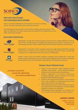
...to reduce cost & ttm
...to provide robustness
	 ...to enhance performance
Solutions Portfolios
TakeCharge® on-chip ESD and EOS protection devices for low voltage CMOS from 0.25um
down to 5nm; for high-speed, low-leakage, low-capacitance, low-noise, RF, analog, over- and
undervoltage tolerance; often combined with beyond standard robustness requirements.
PowerQubic® on-chip ESD and EOS protection devices for high voltage CMOS/BCD, typically
0.35um down to 0.18um and 5V to 50V; for automotive, industrial; mostly requiring high
robustness for a combination of harsh ESD, EOS, LU and EMI specs.
PhyStar® robust circuit and interface solutions, including custom analog I/O’s, circuits that
handle transient disturbances (e.g. to provide antenna clipping or POR), as well as automotive
standard PHYs (e.g. a full LIN PHY with integrated ESD, EOS and EMC robustness).
CONTACT SOFICS
bd@sofics.mail.com
www.sofics.com
SOFICS BVBA
©2019
ON-CHIP SOLUTIONS
FOR ESD/EOS/LATCH UP/EMC
Sofics is a foundry independent semiconductor IP company providing
custom, specialty analog I/Os and on-chip ESD protection.
Our technology is characterized on 10 foundries including advanced nodes at TSMC,
UMC, GF, TowerJazz. Our silicon design and circuit solutions are complementary to the
public and foundry solutions.
Unique Value Propositions
•	 Enable on-chip robustness while supporting normal
operation requirements – where standard solutions
introduce loss of functionality or performance.
•	 Enable IC applications in very harsh environments
(including radiation, system transients) with much
beyond standard ESD/EOS protection.
•	 Providearecurringeconomicbenefit–suchasreduced
silicon area, avoidance of dedicated/special process
steps/masks, first time right tape-outs.
•	 Mass production proven solutions without full cost of,
and extensive time for development, shuttles, product
integration and prior art verification.
•	 Predeveloped solution portfolios at a fraction of the
cost, and with recurring benefits to Sofics customer.
12nm
16nm
22nm
5nm
7nm
28nm
40nm
65nm
90nm
130nm
180nm
250nm
350nm
GF IDM TSMC UMC GF SMIC FUJITSU TJ LFOUNDRY GRACE SILTERRA ALTIS IDM TSMC UMC TJ IDM
Bulk CMOS BCDSOI
Silicon Proven
Silicon in Sofics’ lab
Por�ng
WIDE IP PORTFOLIO ACROSS TECHNOLOGY NODES

On-Chip Solutions for ESD/EOS/Latch up/EMC

  • 1.
    ...to reduce cost& ttm ...to provide robustness ...to enhance performance Solutions Portfolios TakeCharge® on-chip ESD and EOS protection devices for low voltage CMOS from 0.25um down to 5nm; for high-speed, low-leakage, low-capacitance, low-noise, RF, analog, over- and undervoltage tolerance; often combined with beyond standard robustness requirements. PowerQubic® on-chip ESD and EOS protection devices for high voltage CMOS/BCD, typically 0.35um down to 0.18um and 5V to 50V; for automotive, industrial; mostly requiring high robustness for a combination of harsh ESD, EOS, LU and EMI specs. PhyStar® robust circuit and interface solutions, including custom analog I/O’s, circuits that handle transient disturbances (e.g. to provide antenna clipping or POR), as well as automotive standard PHYs (e.g. a full LIN PHY with integrated ESD, EOS and EMC robustness). CONTACT SOFICS bd@sofics.mail.com www.sofics.com SOFICS BVBA ©2019 ON-CHIP SOLUTIONS FOR ESD/EOS/LATCH UP/EMC Sofics is a foundry independent semiconductor IP company providing custom, specialty analog I/Os and on-chip ESD protection. Our technology is characterized on 10 foundries including advanced nodes at TSMC, UMC, GF, TowerJazz. Our silicon design and circuit solutions are complementary to the public and foundry solutions. Unique Value Propositions • Enable on-chip robustness while supporting normal operation requirements – where standard solutions introduce loss of functionality or performance. • Enable IC applications in very harsh environments (including radiation, system transients) with much beyond standard ESD/EOS protection. • Providearecurringeconomicbenefit–suchasreduced silicon area, avoidance of dedicated/special process steps/masks, first time right tape-outs. • Mass production proven solutions without full cost of, and extensive time for development, shuttles, product integration and prior art verification. • Predeveloped solution portfolios at a fraction of the cost, and with recurring benefits to Sofics customer.
  • 2.
    12nm 16nm 22nm 5nm 7nm 28nm 40nm 65nm 90nm 130nm 180nm 250nm 350nm GF IDM TSMCUMC GF SMIC FUJITSU TJ LFOUNDRY GRACE SILTERRA ALTIS IDM TSMC UMC TJ IDM Bulk CMOS BCDSOI Silicon Proven Silicon in Sofics’ lab Por�ng WIDE IP PORTFOLIO ACROSS TECHNOLOGY NODES