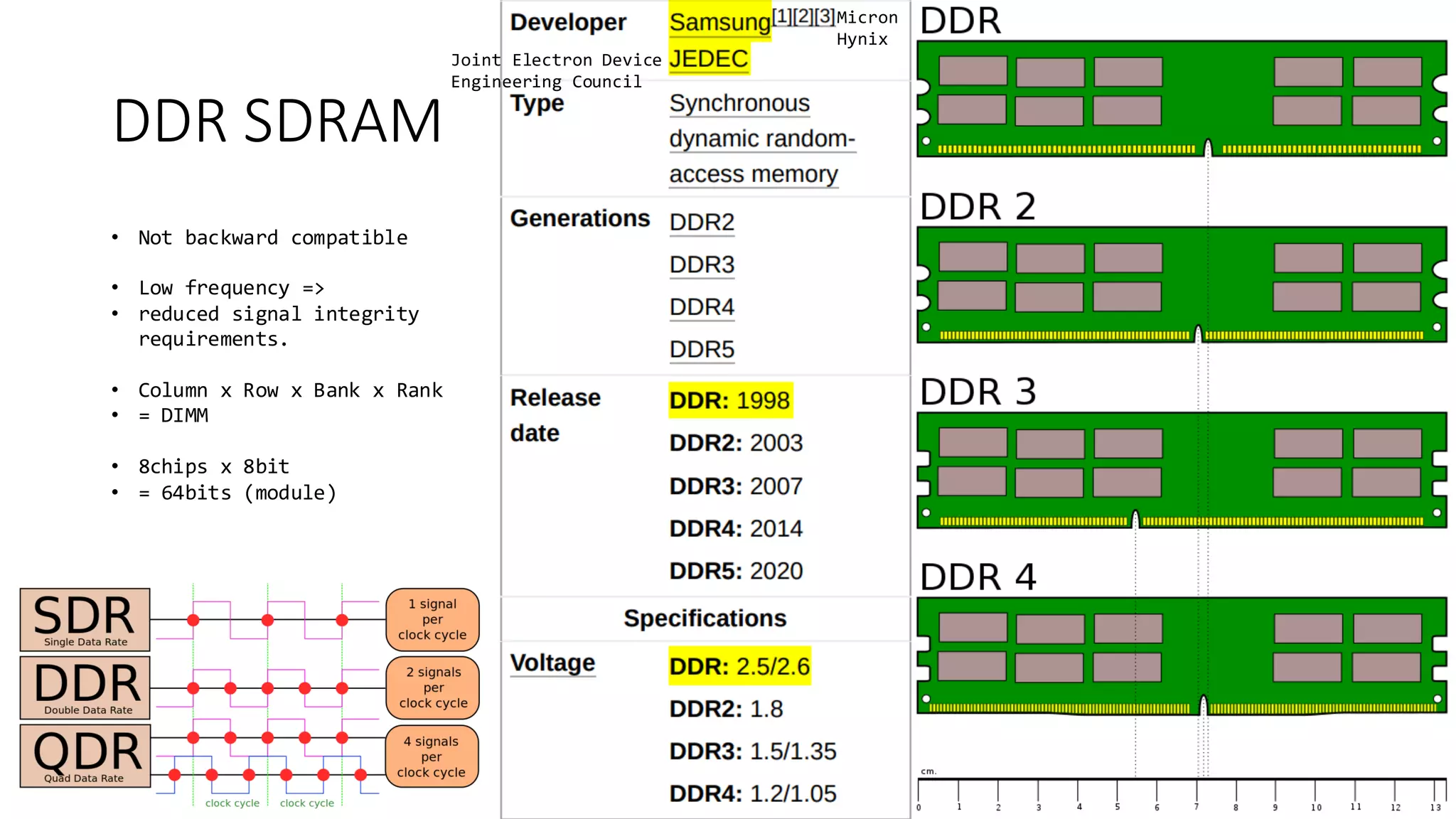
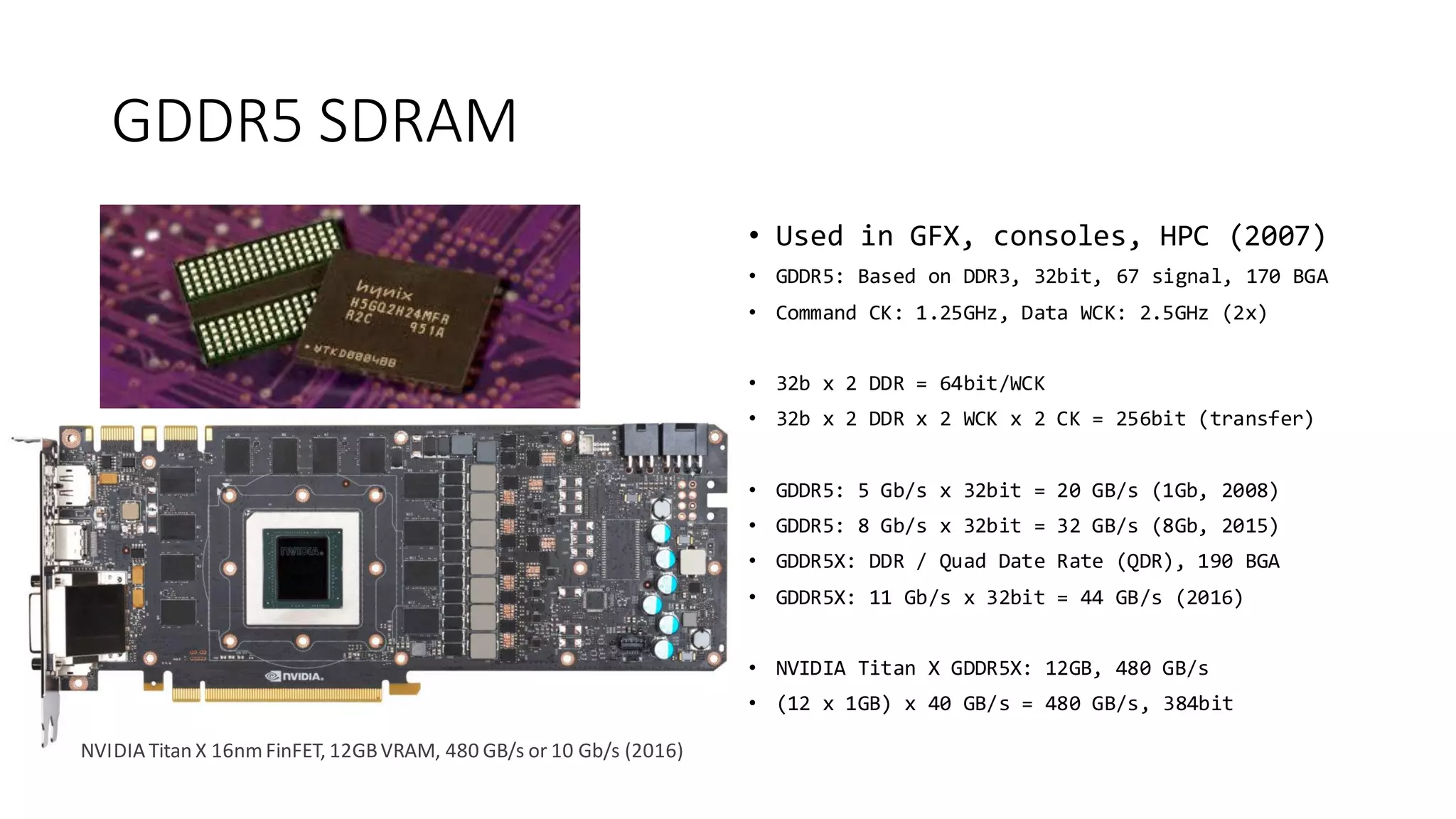
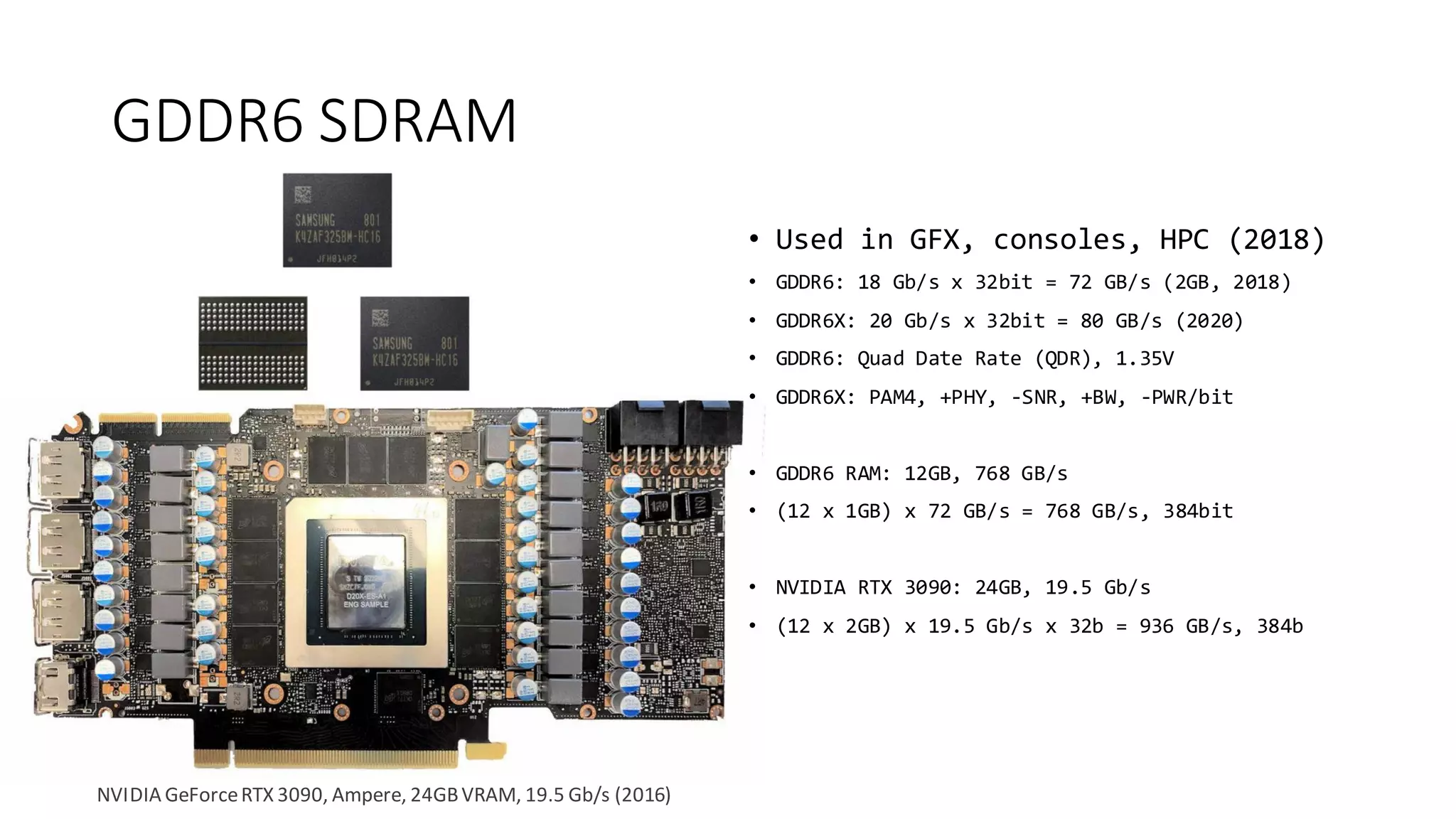
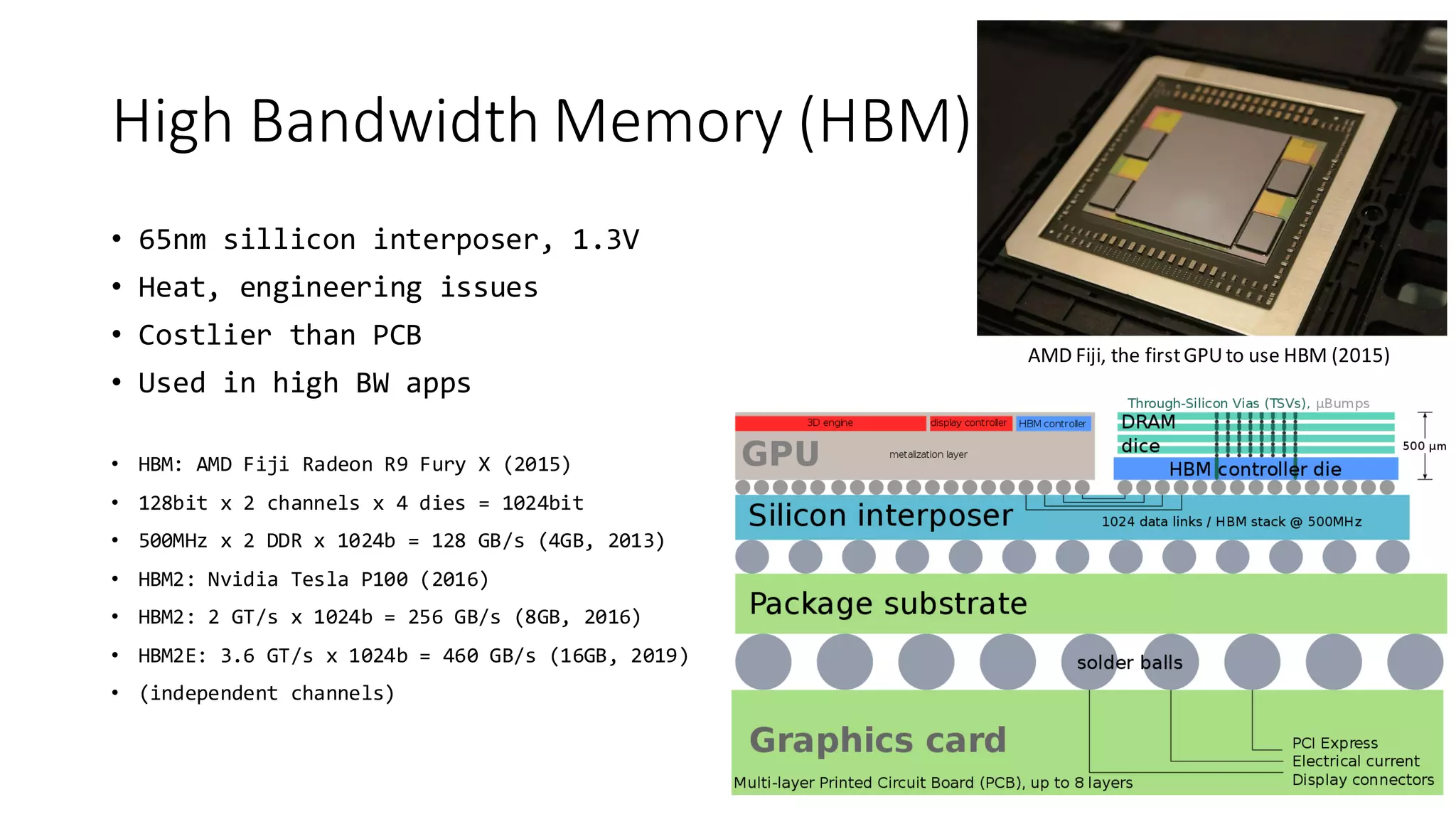
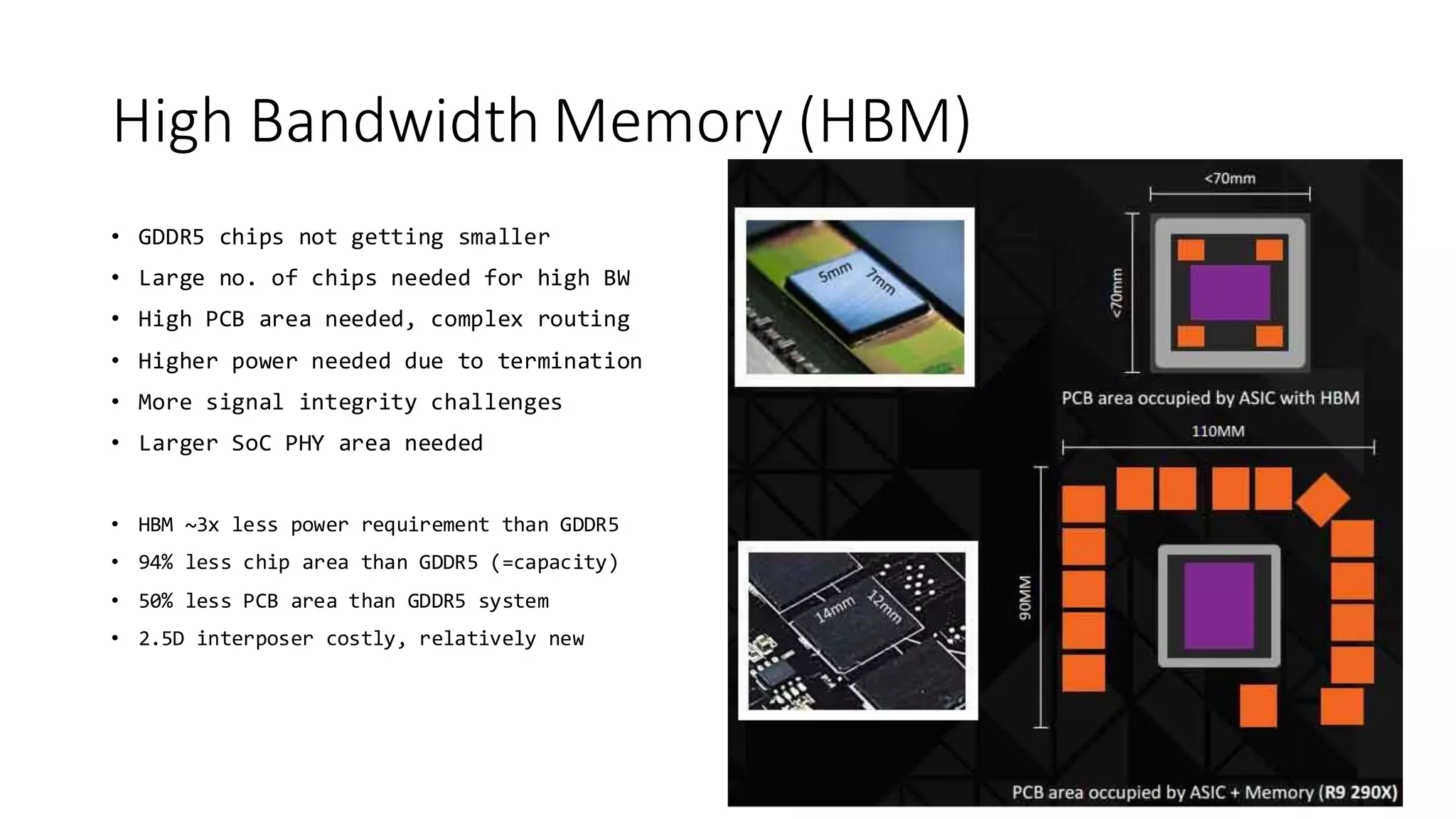
Micron
Hynix
DDR SDRAM
• Not backward compatible
• Low frequency =>
• reduced signal integrity
requirements.
• Column x Row x Bank x Rank
• = DIMM
• 8chips x 8bit
• = 64bits (module)
Joint Electron Device
Engineering Council
DDR3 SDRAM
• Upto 16GB, 1GB/chip, 1.5V (2005)
• CL-RCD-RP: col. delay, row delay, prech. delay
• BW: mem CK x 4 bus mult. X 2 DDR x 64b
• eXtended Memory Profile (XMP, 2007)
• DDR3L: 1.35V (2010), DDR3U: 1.25V (2011)
• DDR4-800: 100MHz mem CK x 4 = 400MHz IO CK
• 400MHz x 2 DDR x 64b = 6.4 GB/s (5-5-5)
• DDR4-2133: 266MHz mem CK x 4 = 1066MHz IO CK
• 1066MHz x 2 DDR x 64b = 17 GB/s (11-11-11)
• Hynix 16GB: (16 x 1GB) 2133MHz x 64b = 17 GB/s
Transcend 4GBECC DDR3 DRAM, 1600 MT/s (2013)
16GBDDR3 SO-DIMM,1600 MT/s, 1.35/1.5V
DDR4 SDRAM
• Upto 64GB, 1.2V, 40-16nm (2011)
• Power: refresh strategies, data bus inv.
• Row hammer: large capacitors, ASLR (addr. rnd.)
• DIMM: 288 pins, 0.85mm spacink
• SO-DIMM: 260 pins, 0.5mm spacing (skylake)
• DDR4-1600: 200MHz mem CK x 4 = 800MHz IO CK
• 800MHz x 2 DDR x 64b = 12.8 GB/s (10-10-10)
• DDR4-3200: 400MHz mem CK x 4 = 1600MHz IO CK
• 1600MHz x 2 DDR x 64b = 25.6 GB/s (20-20-20)
• Hynix 16GB: (16 x 1GB) 2133MHz x 64b = 17 GB/s
Samsung 2GBECC DDR4 DRAM, 2133 MT/s, 1.2V (2011)
GOOD RAM16GBDDR4 DRAM, 2133 MT/s, 1.2V
Registered Memory (RDIMM)
• For high-density chips (36)
• +1 cycle latency
• Normally features ECC
• Costlier, used in servers
• Motherboard must support
• RDIMM: +address, +command
• LRDIMM: +data (+capacity)
Two 8 GB DDR4-2133 ECC 1.2 V RDIMMs
ECC Memory
• Immune to 1bit errors (/64bits)
• Servers: scientific, finance, L1-L2
• Error => crash, data corr., sec.
• Row hammer: security exploit
• Electrical, magnetic interference
• Cosmic secondaries – neutrons
• 1.5km: 3.5x, 10km: 300x
• Cassini-Huygens: =112/Gb/day
• Google servers: 1.67/Gb/day
• Doesn’t inc. with dec. Size
• Hamming code, Chipkill ECC (interleaved)
• Non-ECC cant correct errorsECC DIMMs typically have9 memory chips on each side
• Rival to Rambus XDR DRAM (2005)
• GDDR4: Based on DDR3, 32bit, 1.5V
• Data Bus Inversion (DBI): -PWR, -GND bounce
• 2.5 Gb/s x 32bit = 10 GB/s (256Mb, 2005)
• 4 Gb/s x 32bit = 16 GB/s (512Mb, 2007)
• AMD Radeon HD 3870 GDDR4: 512MB, 72 GB/s
• 1126MHz mem clock x 2 DDR = 2.25 Gb/s
• (8 x 512Mb) x 2.25 Gb/s x 32b = 72 GB/s, 256bit
GDDR4 SDRAM
ATi Radeon HD 3870 512MBVRAM, 72 GB/s, 256bit(2007)
• Used in GFX, consoles, HPC (2007)
• GDDR5: Based on DDR3, 32bit, 67 signal, 170 BGA
• Command CK: 1.25GHz, Data WCK: 2.5GHz (2x)
• 32b x 2 DDR = 64bit/WCK
• 32b x 2 DDR x 2 WCK x 2 CK = 256bit (transfer)
• GDDR5: 5 Gb/s x 32bit = 20 GB/s (1Gb, 2008)
• GDDR5: 8 Gb/s x 32bit = 32 GB/s (8Gb, 2015)
• GDDR5X: DDR / Quad Date Rate (QDR), 190 BGA
• GDDR5X: 11 Gb/s x 32bit = 44 GB/s (2016)
• NVIDIA Titan X GDDR5X: 12GB, 480 GB/s
• (12 x 1GB) x 40 GB/s = 480 GB/s, 384bit
GDDR5 SDRAM
NVIDIA Titan X 16nmFinFET, 12GBVRAM, 480 GB/s or 10 Gb/s (2016)
• Used in GFX, consoles, HPC (2018)
• GDDR6: 18 Gb/s x 32bit = 72 GB/s (2GB, 2018)
• GDDR6X: 20 Gb/s x 32bit = 80 GB/s (2020)
• GDDR6: Quad Date Rate (QDR), 1.35V
• GDDR6X: PAM4, +PHY, -SNR, +BW, -PWR/bit
• GDDR6 RAM: 12GB, 768 GB/s
• (12 x 1GB) x 72 GB/s = 768 GB/s, 384bit
• NVIDIA RTX 3090: 24GB, 19.5 Gb/s
• (12 x 2GB) x 19.5 Gb/s x 32b = 936 GB/s, 384b
GDDR6 SDRAM
NVIDIA GeForceRTX 3090, Ampere, 24GBVRAM, 19.5 Gb/s (2016)
High Bandwidth Memory (HBM)
• 65nm sillicon interposer, 1.3V
• Heat, engineering issues
• Costlier than PCB
• Used in high BW apps
• HBM: AMD Fiji Radeon R9 Fury X (2015)
• 128bit x 2 channels x 4 dies = 1024bit
• 500MHz x 2 DDR x 1024b = 128 GB/s (4GB, 2013)
• HBM2: Nvidia Tesla P100 (2016)
• HBM2: 2 GT/s x 1024b = 256 GB/s (8GB, 2016)
• HBM2E: 3.6 GT/s x 1024b = 460 GB/s (16GB, 2019)
• (independent channels)
AMD Fiji, the firstGPUto use HBM (2015)
High Bandwidth Memory (HBM)
• GDDR5 chips not getting smaller
• Large no. of chips needed for high BW
• High PCB area needed, complex routing
• Higher power needed due to termination
• More signal integrity challenges
• Larger SoC PHY area needed
• HBM ~3x less power requirement than GDDR5
• 94% less chip area than GDDR5 (=capacity)
• 50% less PCB area than GDDR5 system
• 2.5D interposer costly, relatively new
Non-Volatile RAM (NVRAM)
• Floating-gate MOSFET
• EPROM, EEPROM, EEPROM+SRAM, Flash
• Phase-change RAM (PCRAM): 3D
XPoint Intel Optane, Micron Quantx
• Ferroelectric RAM (FeRAM)
• Magnetoresistive RAM (MRAM)
• Electrochemical RAM (ECRAM)
• Resistive RAM (ReRAM)
• Can be fully-powered down
• For in-memory analog mat-mul (DNN)
Two Intel Optane 256GB DDR4 DIMMs with AES-256 (2019)
Serial Presence Detect (SPD)
• Standardized way to automatically
access information about a memory
module
• What memory timings to use to
access the memory
• Overclocking: over-ride SPD data
• Accessed using SMBus, a variant of the I²C
protocol
• SMBus: System Monitor - power supply, CPU
temp., fan speeds.
• XMP uses bytes 176–255, unallocated by JEDEC, to
encode higher-performance memory timings. Memory device on an SDRAM module, containing SPD data
DDR PHY Training
DDR, GDDR, HBM Memory : Presentation

DDR, GDDR, HBM Memory : Presentation

  • 1.
    Micron Hynix DDR SDRAM • Notbackward compatible • Low frequency => • reduced signal integrity requirements. • Column x Row x Bank x Rank • = DIMM • 8chips x 8bit • = 64bits (module) Joint Electron Device Engineering Council
  • 2.
    DDR3 SDRAM • Upto16GB, 1GB/chip, 1.5V (2005) • CL-RCD-RP: col. delay, row delay, prech. delay • BW: mem CK x 4 bus mult. X 2 DDR x 64b • eXtended Memory Profile (XMP, 2007) • DDR3L: 1.35V (2010), DDR3U: 1.25V (2011) • DDR4-800: 100MHz mem CK x 4 = 400MHz IO CK • 400MHz x 2 DDR x 64b = 6.4 GB/s (5-5-5) • DDR4-2133: 266MHz mem CK x 4 = 1066MHz IO CK • 1066MHz x 2 DDR x 64b = 17 GB/s (11-11-11) • Hynix 16GB: (16 x 1GB) 2133MHz x 64b = 17 GB/s Transcend 4GBECC DDR3 DRAM, 1600 MT/s (2013) 16GBDDR3 SO-DIMM,1600 MT/s, 1.35/1.5V
  • 3.
    DDR4 SDRAM • Upto64GB, 1.2V, 40-16nm (2011) • Power: refresh strategies, data bus inv. • Row hammer: large capacitors, ASLR (addr. rnd.) • DIMM: 288 pins, 0.85mm spacink • SO-DIMM: 260 pins, 0.5mm spacing (skylake) • DDR4-1600: 200MHz mem CK x 4 = 800MHz IO CK • 800MHz x 2 DDR x 64b = 12.8 GB/s (10-10-10) • DDR4-3200: 400MHz mem CK x 4 = 1600MHz IO CK • 1600MHz x 2 DDR x 64b = 25.6 GB/s (20-20-20) • Hynix 16GB: (16 x 1GB) 2133MHz x 64b = 17 GB/s Samsung 2GBECC DDR4 DRAM, 2133 MT/s, 1.2V (2011) GOOD RAM16GBDDR4 DRAM, 2133 MT/s, 1.2V
  • 4.
    Registered Memory (RDIMM) •For high-density chips (36) • +1 cycle latency • Normally features ECC • Costlier, used in servers • Motherboard must support • RDIMM: +address, +command • LRDIMM: +data (+capacity) Two 8 GB DDR4-2133 ECC 1.2 V RDIMMs
  • 5.
    ECC Memory • Immuneto 1bit errors (/64bits) • Servers: scientific, finance, L1-L2 • Error => crash, data corr., sec. • Row hammer: security exploit • Electrical, magnetic interference • Cosmic secondaries – neutrons • 1.5km: 3.5x, 10km: 300x • Cassini-Huygens: =112/Gb/day • Google servers: 1.67/Gb/day • Doesn’t inc. with dec. Size • Hamming code, Chipkill ECC (interleaved) • Non-ECC cant correct errorsECC DIMMs typically have9 memory chips on each side
  • 6.
    • Rival toRambus XDR DRAM (2005) • GDDR4: Based on DDR3, 32bit, 1.5V • Data Bus Inversion (DBI): -PWR, -GND bounce • 2.5 Gb/s x 32bit = 10 GB/s (256Mb, 2005) • 4 Gb/s x 32bit = 16 GB/s (512Mb, 2007) • AMD Radeon HD 3870 GDDR4: 512MB, 72 GB/s • 1126MHz mem clock x 2 DDR = 2.25 Gb/s • (8 x 512Mb) x 2.25 Gb/s x 32b = 72 GB/s, 256bit GDDR4 SDRAM ATi Radeon HD 3870 512MBVRAM, 72 GB/s, 256bit(2007)
  • 7.
    • Used inGFX, consoles, HPC (2007) • GDDR5: Based on DDR3, 32bit, 67 signal, 170 BGA • Command CK: 1.25GHz, Data WCK: 2.5GHz (2x) • 32b x 2 DDR = 64bit/WCK • 32b x 2 DDR x 2 WCK x 2 CK = 256bit (transfer) • GDDR5: 5 Gb/s x 32bit = 20 GB/s (1Gb, 2008) • GDDR5: 8 Gb/s x 32bit = 32 GB/s (8Gb, 2015) • GDDR5X: DDR / Quad Date Rate (QDR), 190 BGA • GDDR5X: 11 Gb/s x 32bit = 44 GB/s (2016) • NVIDIA Titan X GDDR5X: 12GB, 480 GB/s • (12 x 1GB) x 40 GB/s = 480 GB/s, 384bit GDDR5 SDRAM NVIDIA Titan X 16nmFinFET, 12GBVRAM, 480 GB/s or 10 Gb/s (2016)
  • 8.
    • Used inGFX, consoles, HPC (2018) • GDDR6: 18 Gb/s x 32bit = 72 GB/s (2GB, 2018) • GDDR6X: 20 Gb/s x 32bit = 80 GB/s (2020) • GDDR6: Quad Date Rate (QDR), 1.35V • GDDR6X: PAM4, +PHY, -SNR, +BW, -PWR/bit • GDDR6 RAM: 12GB, 768 GB/s • (12 x 1GB) x 72 GB/s = 768 GB/s, 384bit • NVIDIA RTX 3090: 24GB, 19.5 Gb/s • (12 x 2GB) x 19.5 Gb/s x 32b = 936 GB/s, 384b GDDR6 SDRAM NVIDIA GeForceRTX 3090, Ampere, 24GBVRAM, 19.5 Gb/s (2016)
  • 9.
    High Bandwidth Memory(HBM) • 65nm sillicon interposer, 1.3V • Heat, engineering issues • Costlier than PCB • Used in high BW apps • HBM: AMD Fiji Radeon R9 Fury X (2015) • 128bit x 2 channels x 4 dies = 1024bit • 500MHz x 2 DDR x 1024b = 128 GB/s (4GB, 2013) • HBM2: Nvidia Tesla P100 (2016) • HBM2: 2 GT/s x 1024b = 256 GB/s (8GB, 2016) • HBM2E: 3.6 GT/s x 1024b = 460 GB/s (16GB, 2019) • (independent channels) AMD Fiji, the firstGPUto use HBM (2015)
  • 10.
    High Bandwidth Memory(HBM) • GDDR5 chips not getting smaller • Large no. of chips needed for high BW • High PCB area needed, complex routing • Higher power needed due to termination • More signal integrity challenges • Larger SoC PHY area needed • HBM ~3x less power requirement than GDDR5 • 94% less chip area than GDDR5 (=capacity) • 50% less PCB area than GDDR5 system • 2.5D interposer costly, relatively new
  • 11.
    Non-Volatile RAM (NVRAM) •Floating-gate MOSFET • EPROM, EEPROM, EEPROM+SRAM, Flash • Phase-change RAM (PCRAM): 3D XPoint Intel Optane, Micron Quantx • Ferroelectric RAM (FeRAM) • Magnetoresistive RAM (MRAM) • Electrochemical RAM (ECRAM) • Resistive RAM (ReRAM) • Can be fully-powered down • For in-memory analog mat-mul (DNN) Two Intel Optane 256GB DDR4 DIMMs with AES-256 (2019)
  • 12.
    Serial Presence Detect(SPD) • Standardized way to automatically access information about a memory module • What memory timings to use to access the memory • Overclocking: over-ride SPD data • Accessed using SMBus, a variant of the I²C protocol • SMBus: System Monitor - power supply, CPU temp., fan speeds. • XMP uses bytes 176–255, unallocated by JEDEC, to encode higher-performance memory timings. Memory device on an SDRAM module, containing SPD data
  • 13.