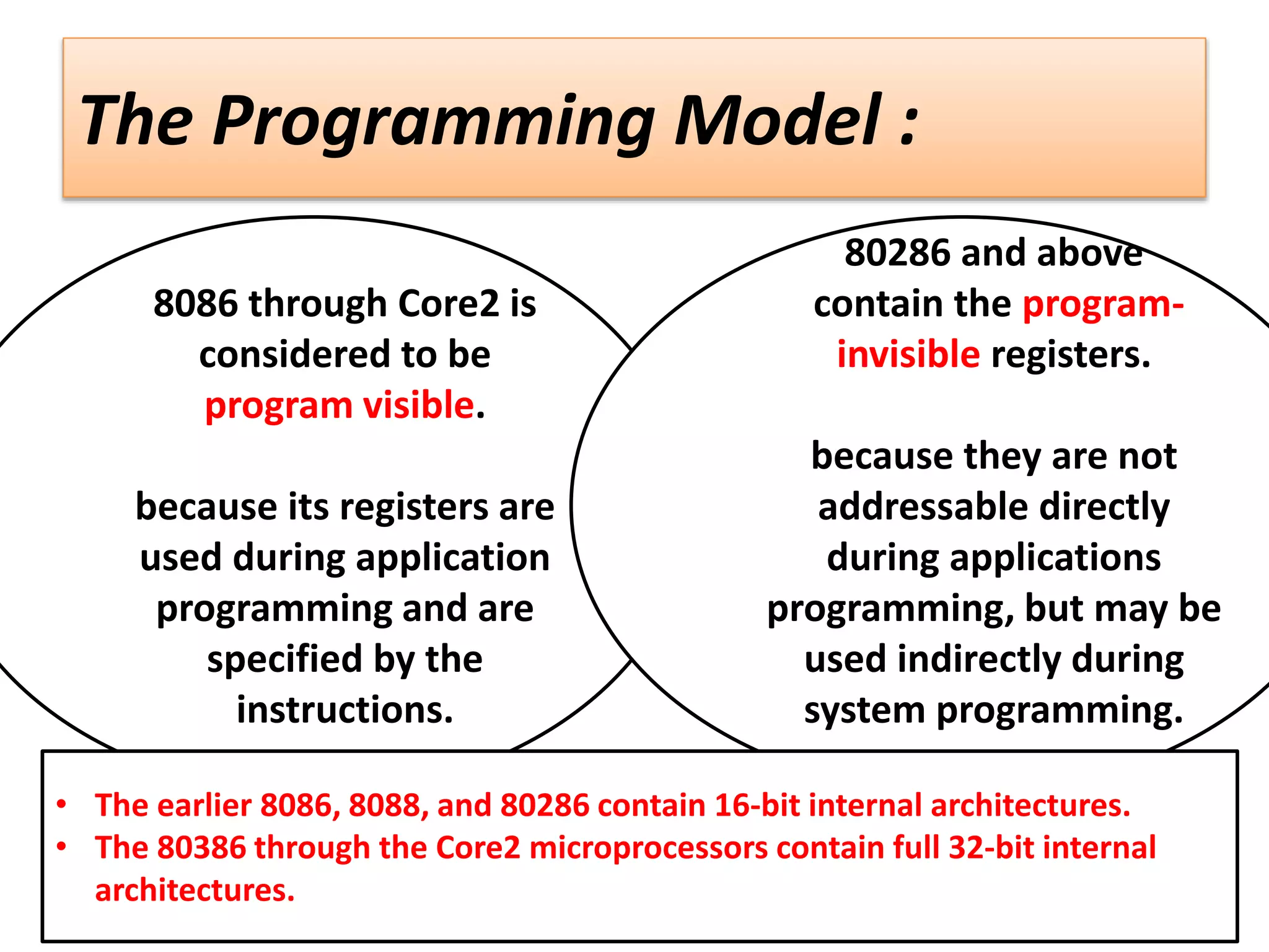
SlideShare a Scribd company logo
Chapter Objectives
• Describe function and purpose of each program-visible
register in the 8086-Core2 microprocessors, including 64-bit
extensions.
• Detail the flag register and the purpose of each flag bit.
• Describe how memory is accessed using real mode memory-
addressing techniques.
• Describe how memory is accessed using protected mode
memory-addressing techniques.
• Describe how memory is accessed using the 64-bit flat
memory model.
• Describe program-invisible registers found in the 80286
through Core2 microprocessors.
• Detail the operation of the memory-paging mechanism.
Introduction
Addressing modes for the powerful family of Intel MPs. are:
1. Real mode memory (DOS memory):
2. Protected mode memory (Windows memory):
3. Flat mode memory:
• at locations 00000H–FFFFFH(the first 1M byte).
• present on all versions of the MPs.
• at any location in the entire protected memory system.
• available only to the 80286–Core2.
• the Pentium 4 and Core2 address 1T byte of memory.
• when the 64-bit extensions are enabled.
Internal Microprocessor Architecture
In a multiple core microprocessor:
• each core contains the
same programming model.
• each core runs a separate
task or thread simultaneously.
The Programming Model :
8086 through Core2 is
considered to be
program visible.
because its registers are
used during application
programming and are
specified by the
instructions.
80286 and above
contain the program-
invisible registers.
because they are not
addressable directly
during applications
programming, but may be
used indirectly during
system programming.
• The earlier 8086, 8088, and 80286 contain 16-bit internal architectures.
• The 80386 through the Core2 microprocessors contain full 32-bit internal
architectures.
the programming model 8086
through Core2 microprocessor
including the 64-bit extensions:
• The earlier 8086, 8088, and
80286 contain 16-bit registers
• These 32-bit extended
registers, and 16-bit registers
are available only in the 80386
and above.
• The Pentium 4 and Core2
also contain 64-bit
registers when operated in
the 64-bit mode.
registers
Segment
registers
Special purpose
registers
General purpose
registers
RAX
RBX
RCX
RDX
RBP
RDI
RSI
R8-R15
RIP
RSP
RFLAGS
CS
DS
ES
SS
FS
GS
General-Purpose Registers:
First group …
RAX RBX RCX RDX
2. RAX is 64-bit ,
EAX is 32-bit ,
AX is 16-bit ,
AH & AL are 8-bit.
1. Accumulator
Register.
1. Count Register.1. Base Register. 1. Data Register.
2. RBX is 64-bit ,
EBX is 32-bit ,
BX is 16-bit ,
BH & BL are 8-bit.
2. RCX is 64-bit ,
ECX is 32-bit ,
ACis 16-bit ,
AC & AC are
8-bit.
2. RDX is 64-bit ,
EDX is 32-bit ,
AD is 16-bit ,
AD & DL are 8-bit.
3. used for instruc-
tions such as MUL
, DIV and others.
3. holds the offset
address of a
location in the
memory system.
3. holds the count
for various
instructions.
3. holds part of the
result from MUL
or part of the
dividend before
a division.
Adding Examples :
1. ADD AL,AH
instruction adds the 8-bit contents of AH to AL. (Only AL
changes due to this instruction.)
2. ADD DX, CX
instruction adds the 16-bit contents of CX to DX. (Only DX
changes due to this instruction.)
3. ADD ECX, EBX
instruction adds the 32-bit contents of EBX to ECX. (Only ECX
changes due to this instruction.)
4. ADD RCX, RBX
instruction adds the 64-bit contents of RBX to RCX. (Only RCX
changes due to this instruction.)
General-Purpose Registers:
Second group …
RBP
2. is addressable as RBP,
EBP, or BP.
1. Base pointer.
3. points to a memory
location in all versions
of the MPs. for
memory data transfers.
RDI
1. Destination index.
2. is addressable as
RDI, EDI, or DI.
3. often addresses string
destination data for the
string instructions.
RSI
1. Source index.
2. is used as RSI, ESI,
or SI.
3. often addresses source
string data for the string
instructions.
General-Purpose Registers:
Third group …
Numbered register(R8 through R15) :
• only found in the Pentium 4 and Core2 if 64-bit extensions
are enabled.
• data in these registers are addressed as 64-, 32-, 16-, or
8-bit sizes.
• note that the 8-bit portion is the rightmost 8-bit only; bits 8
to 15 are not directly addressable as a byte.
Flat mode 64-bit access to numbered
registers:
Special-Purpose Registers:
• addresses the next instruction in a section of memory defined
as (instruction pointer) a code segment.
• This register is IP (16 bits) when the microprocessor operates
in the real mode and EIP (32 bits) when the 80386 and above
operate in the protected mode.
• the 8086, 8088, and 80286 do not contain an EIP register.
• In the 64-bit mode, RIP contains a 40-bit address at present
to address a 1T flat address space.
RIP (instruction pointer):
RSP (stack pointer) :
• addresses an area of memory called the stack.
• The stack memory stores data through this pointer.
• This register is referred to as SP if used as a 16-bit register
and ESP if referred to as a 32-bit register.
ID X ID Flag (CPUID support)
VIP X Virtual Interrupt Pending
VIF X Virtual Interrupt Flag
AC X Alignment Check
VM X Virtual 8086 Mode
RF X Resume Flag
NT X Nested Task
IOPL X I/O Privilege Level
OF S Overflow Flag
DF C Direction Flag
IF X Interrupt Enable Flag
TF X Trap Flag
SF S Sign Flag
ZF S Zero Flag
AF S Auxiliary Carry Flag
PF S Parity Flag
CF S Carry Flag
S = Status Flag
C = Control Flag
X = System Flag
Bit Positions shown as “0” or “1” are
Intel reserved.
31 0
0 0 0 0 0 0 0 0 0 0
I
D
V
I
P
V
I
F
A
C
V
M
R
F
0
N
T
I
O
P
L
I
O
P
L
O
F
D
F
I
F
T
F
S
F
Z
F
0
A
F
0
P
F
21
1
15 7
C
F
7
0
EFLAG register
RFLAGS :
• indicate the condition of the microprocessor and control its
operation.
• Flags are upward-compatible from the 8086/8088 through Core2 .
• The rightmost five and the overflow flag are changed by most
arithmetic and logic operations.
• Note that the data transfers do not affect them.
• Flags never change for any data transfer or program control
operation.
• Some of the flags are also used to control features found in the
microprocessor.
• The 8086–80286 contain a FLAG register (16 bits) and the 80386
and above contain an EFLAG register (32-bit extended flag
register).
EFlag bits, with a brief description of each flag
function:
holds the carry (half-carry) after addition or the borrow after
subtraction between bit positions 3 and 4 of the result.
holds the carry after addition or borrow after subtraction.
 also indicates error conditions.
Logic 1 for even parity.
Logic 0 for odd parity.
A=1, there is carry out from bit3 in addition or borrow
into bit3 in subtraction.
Otherwise A=0.
1. C (carry):
2. P (parity):
is the count of ones in a number expressed as even or odd.
3. A (auxiliary carry):
4. Z (zero):
shows that the result of an arithmetic or logic operation
is zero.
5. S (sign):
flag holds the arithmetic sign of the result after an
arithmetic or logic instruction executes.
 if S=1, the number is negative.
 if S=0, the number is positive.
6. T (trap):
The trap flag enables trapping through an on-chip debugging
feature.
 If T=1, cause inttrupt after the execution of each instruction
used for debugging.
 If T=0, the trapping (debugging) feature is disabled.
7. I (interrupt):
controls operation of the INTR (interrupt request)
input pin.
 If I=1, the INTR pin is enabled.
 if I=0, the INTR pin is disabled.
8. D (direction):
selects increment or decrement mode for the DI
and/or SI registers.
• If D=1, the registers are automatically decremented.
• if D=0, the registers are automatically incremented.
9. O (overflow):
occurs when signed numbers are added or subtracted.
 an overflow indicates the result has exceeded
the capacity of the machine
9. IOPL (I/O privilege level):
used in protected mode operation to select the privilege level for
I/O devices.
 If the IOPL is lower than the current privilege level, an
interrupt occurs, causing execution to suspend.
 Note that an IOPL of 00 is the highest or most trusted and an
IOPL of 11 is the lowest or least trusted.
10. NT (nested task):
flag indicates the current task is nested within another task
in protected mode operation.
 set when the task is nested by software.
11. RF (resume):
used with debugging to control resumption of execution
after the next instruction.
12. VM (virtual mode):
flag bit selects virtual mode operation in a protected mode
system.
13. AC(alignment check):
flag bit activates if a word or doubleword is
addressed on a non-word or non-doubleword boundary.
14. VIF(virtual interrupt):
is a copy of the interrupt flag bit available to the
Pentium4 MP.
15. VIP (virtual interrupt pending):
provides information about a virtual mode interrupt
for Pentium-Pentium4.
 used in multitasking environments to provide virtual
interrupt flags.
16.ID (identification):
flag indicates that the Pentium microprocessors
support the CPUID instruction.
 CPUID instruction provides the system with
information about the Pentium microprocessor.
Segment Registers:
• Generate memory addresses when
combined with other registers in the
microprocessor.
• Four or six segment registers in various
versions of the microprocessor.
(The 8086–80286 microprocessors allow
four memory segments and the 80386–
Core2 microprocessors allow six memory
segments.
• A segment register functions differently in real mode than
in protected mode.
1. CS (code):
segment holds code (programs and procedures) used by the
microprocessor.
2. DS (data):
contains most data used by a program.
 Data are accessed by an offset address or contents of
other registers that hold the offset address.
3. ES (extra):
an additional data segment used by some instructions to
hold destination data.
4. SS (stack):
defines the area of memory used for the stack.
stack entry point is determined by the stack segment
and stack pointer registers.
the BP register also addresses data within
the stack segment .
5. FS and GS:
segments are supplemental segment registers available in
80386–Core2 microprocessors.
– allow two additional memory segments for
access by programs
• Windows uses these segments for internal operations,
but no definition of their usage is available.
Real Mode Memory Addressing
• This mode allows the microprocessor to address only the
first 1M byte of memory space.
• Is called conventional memory, or DOS memory system
• The DOS operating system requires that the
microprocessor operates in the real mode. Windows does
not use the real mode.
• The 80286 and above operate in either the real or
protected mode.
• Only the 8086 and 8088 operate exclusively in the real
mode.
• In the 64-bit operation mode of the Pentium 4 and Core2,
there is no real mode operation. it cannot execute real
mode applications.
Segments and Offsets:
• To access a memory location in the real mode, a
combination of a segment address and an offset
address is needed.
• The segment address, located within one of the
segment registers, defines the beginning address of
any 64K-byte memory segment.
• The offset address(displacement), is the distance
above the start of the segment selects any location
within the 64K byte memory segment.
• the segment plus offset generate a 20-bit memory
address to access a location within the first 1M of
memory.
• the ending address is found by adding FFFFH.
Memory Address Generation
Physical Address (20 Bits)
Adder
Segment Register (16 bits) 0 0 0 0
Offset Value (16 bits)
The real mode memory-addressing scheme,
using a segment address plus an offset:
Example:
if a segment register contains 3000H, and the
offset is F000H (3000:F000)
Thus…
the first address of the segment is 30000H.
the physical address= 30000H+F000H= 3F000H.
the ending address is 30000H+FFFFH= 3FFFFH.
Examples of real mode segment
addresses:
Some addressing modes combine more than one register and
an offset value to form an offset address.
When this occurs, the sum of these values may exceed FFFFH.
For Example…
segment address is 4000H and offset address is specified as the
sum of F000H plus 3000H
Offset= F000H+3000H=12000H, which greater than FFFFH.
So that the carry of 1 is dropped for this addition to form the
offset address of 2000H.
Physical address= 40000H+2000H=42000H, and not 52000H
which is cause the system to halt and indicate an addressing
error.
Default Segment and Offset Registers:
The physical address is the combination of CS:IP or CS:EIP,
depending upon the microprocessor’s mode of operation.
• The code segment register defines the start of the code
segment.
• The instruction pointer locates the next instruction within
the code segment.
Another of the default combinations is the stack.
• stack data are referenced through the stack segment at
the memory location addressed by either the stack
pointer SP:ESP or the pointer BP:EBP.
4 Segments in
8086
• Code Segment (CS)
• Data Segment (DS)
• Stack Segment (SS)
• Extra Segment (ES)
16 bits Segment Registers & Offset Registers
Default 32-bit segment and offset combinations:
A memory system showing the
placement of four memory
segments:
NOTE: When this program is placed in the
memory system by DOS, it is loaded in
the TPA at the first available area of
memory above the drivers and other TPA
program. This area is indicated by a free-
pointer that is maintained by DOS.
Program loading is handled
automatically by the program loader
located within DOS.
An application program
containing a code, data, and
stack segment loaded into a
DOS system memory.
Note : A segment starts at a
particular address and its
maximum size can go up to
64 Kbytes. But if another
segment starts along this 64
Kbytes location of the first
segment, the two segments
are said to be overlapping
segment.
Segment and Offset Addressing
Scheme Allows Relocation
• Segment plus offset addressing allows DOS
programs to be relocated in memory.
• A relocatable program is one that can be placed into
any area of memory and executed without change.
• Relocatable data are data that can be placed in any
area of memory and used without any change to the
program.
• Because memory is addressed within a segment by
an offset address, the memory segment can be
moved to any place in the memory system without
changing any of the offset addresses.
• Only the contents of the segment register must be
changed to address the program in the new area of
memory.
Protected Mode Memory Addressing
• Allows access to data and programs located within & above
the first 1M byte of memory.
• The offset address is still used to access information
located within the memory segment.
• In place of the segment address, the segment register
contains:
• in the 80386 and above, is that the offset address can be a
32-bit (4G byte) number instead of a 16-bit (64k byte).
• protected mode instructions are identical to real mode
instructions.
 selector that selects a descriptor from a descriptor
table.
 descriptor describes the memory segment’s location,
length, access rights.
Selectors and Descriptors
The selector, located in the segment register, selects one of
descriptors from one of two tables of descriptors.
The descriptor (8 bytes), describes the location, length, and
access rights of the segment of memory. There are 2 descriptor
tables:
 Each descriptor table contains 8192 descriptors. So total
descriptors is 16,384, and the application could have access
to 4G X 16,384 = 64T bytes.
 In protected mode, this segment number can address any
memory location in the system for the code segment.
1. Global descriptors: “system descriptor” contain segment
definitions that apply to all programs.
2. Local descriptors: “application descriptor” usually unique
to an application.
The 80286 through Core2 64-bit descriptors:
1. The base address portion of the descriptor indicates the starting
location of the memory segment
Note: the base address is a 24-bit address, so segments begin
at any location in its 16M bytes of memory and The 80386 and above use
a 32-bit base address that allows segments to begin at any location in its
4G bytes of memory
2. The segment limit contains the last offset address found in a segment
Example…
if a segment begins at memory location F00000H and ends at location
F000FFH.
the base address is F00000H
the limit = end loc. – base add. = FFH.
 For the 80286 microprocessor” 16-bit limit “:
the base address is F00000H and the limit is 00FFH.
 For the 80386 and above” 20-bit limit”,
the base address is 00F00000H and the limit is 000FFH.
3. the G bit(granularity bit): found in the 80386 through the Pentium 4
descriptor that is not found in the 80286 descriptor.
Example1… shows the segment start and end if the base address is
10000000H, the limit is 001FFH, and the G=0
Solution…
Base = Start = 10000000H
End = Base + Limit = 10000000H + 001FFH = 100001FFH
Example2… uses the same data in the previous Example, except that the
G=1.
Solution…
Base = Start = 10000000H
End = Base + Limit = 10000000H + 001FFFFFH = 101FFFFFH
Notice that the limit is appended with FFFH to determine the ending
segment address.
If G=0, the limit specifies a segment limit of 00000H to FFFFFH.
If G=1, the value of the limit is multiplied by 4K bytes
(appended with FFFH).The limit is then 00000FFFFH to FFFFFFFFH
4. the L bit (probably means large, but Intel calls it the 64-bit):
5. The AV bit, in the 80386 and above descriptor, is used by
some operating systems to indicate whether the segment is
available or not.
6. The D bit, indicates how the 80386 through the Core2
instructions access register and memory data in the protected
or real mode.
when L = 1, selects 64-bit extentions addresses in a Pentium
4 or Core2 with 64-bit extensions.
when L=0, 32-bit compatibility mode.
when AV = 1, segment is available.
when AV= 0, segment is not available.
when D = 1, the instructions are 32-bit instructions.
when D= 0, the instructions are 16-bit instructions.
7. The access rights byte:
Note… If the segment grows beyond its limit,
the MP’s operating system program is interrupted,
indicating a general protection fault.
controls access to the protected mode segment.
 describes how the segment functions in the system.
allows complete control over the segment. 64-bit mode there
is only a code
segment and no
other segment
descriptor types.
The contents of a segment register during protected mode
operation of the 80286 through Core2 microprocessors:
DS
0008
Descriptor 0
Descriptor 1
Descriptor 2
Descriptor 3
Descriptor 4
Descriptor 5
Descriptor 6
Descriptor 7
Descriptor 8
Descriptor 9
Descriptor 10
Descriptor 11
63 0
Using the DS register to select a description from the global
descriptor table:
1. DS contains 0008H, which
accesses the descriptor number
1 from the global descriptor table.
2. using a requested privilege level
of 00.
3. Descriptor number 1 contains a
descriptor that defines the base
address as 00100000H with a
segment limit of 000FFH.
4. This means that a value of
0008H loaded into DS causes
the microprocessor to use
memory locations 00100000H–
001000FFH for the data
segment
the DS register accesses memory locations 00100000H–001000FFH as
a data segment.
• To access & specify the table addresses in
80286–Core2.
• control the microprocessor when operated in
protected mode.
• The program-invisible portion of segment
registers is often called cache memory because
cache is any memory that stores information.
• The program-invisible portion of the segment
register is loaded with the base address, limit,
and access rights each time the number segment
register is changed.
Program-Invisible Registers
The program-invisible register within the 80286–Core2
microprocessors:
• The GDTR (global descriptor table register) and IDTR
(interrupt descriptor table register) contain the base address
of the descriptor table and its limit.
• when protected mode operation desired, address of the
global descriptor table and its limit are loaded into the GDTR.
• Before using the protected mode, the interrupt descriptor
table and the IDTR must also be initialized.
• The location of the local descriptor table is selected from the
global descriptor table.
• one of the global descriptors is set up to address the local
descriptor table
• To access the local descriptor table, the LDTR (local
descriptor table register) is loaded with a selector.
selector accesses global descriptor table, & loads
local descriptor table address, limit, & access
rights into the cache portion of the LDTR.
• The TR (task register) holds a selector, which
accesses a descriptor that defines a task.
a task is most often a procedure or application
• The task switch allows multitasking systems to
switch tasks to another in a simple and orderly
fashion.
 located within the 80386 and above, in both the real and protected
modes.
 With memory paging, the linear address is invisibly translated to
any physical address.
 Iinear address is defined as the address generated by a program.
 Physical address is the actual memory location accessed by a
program.
MEMORY PAGING
 The paging unit is controlled by the contents of the
microprocessor’s control registers.
Paging Registers
1. CR4, controls extensions to the basic architecture
provided in the Pentium or newer
microprocessor.
1. CR0 and CR3, are the registers important to the
paging unit.
2. CR3, contains the page directory base or root
address.
3. (PG) bit, selects paging when placed at a logic
1 level.
5. The PCD and PWT bits, control the operation
of the PCD and PWT pins on the microprocessor.
6. The page directory base address, locates the
directory for the page translation unit, contains 1024
directory entries of 4 bytes.
The format for the linear address
offset into
page-frame
index into
page-directory
index into
page-table
31 22 21 12 11 0
10-bits 10-bits 12-bits
This field selects
one of the 1024
array-entries in
the Page-Directory
This field selects
one of the 1024
array-entries in
that Page-Table
This field provides
the offset to one
of the 4096 bytes
in that Page-Frame
Format of a Page-Table entry
PAGE-FRAME BASE ADDRESS PWU
P
W
T
P
C
D
AD00
31 12 11 10 9 8 7 6 5 4 3 2 1 0
AVAIL
LEGEND:
P = Present (1=yes, 0=no)
W = Writable (1 = yes, 0 = no)
U = User (1 = yes, 0 = no)
A = Accessed (1 = yes, 0 = no)
D = Dirty (1 = yes, 0 = no)
PWT = Page Write-Through (1=yes, 0 = no)
PCD = Page Cache-Disable (1 = yes, 0 = no)
The Page Directory and Page Table
• Only one page directory in the system.
• The page directory contains 1024 doubleword
addresses that locate up to 1024 page tables.
• Page directory and each page table are 4K
bytes in length
• Each entry in the page directory corresponds to
4M bytes of physical memory.
• Each entry in the page table repages 4K bytes of
physical memory.
The paging mechanism in the 80386 through
Core2 microprocessors.
The page directory, page
table 0, and two memory
pages.
Note: how the address of
page 000C8000–000C9000
has been moved to
00110000–00110FFF.
• A flat mode memory system is one in
which there is no segmentation.
– does not use a segment register to address a
location in the memory
• First byte address is at 00 0000 0000H;
the last location is at FF FFFF FFFFH.
– address is 40-bits
• The segment register still selects the
privilege level of the software.
Flat Mode Memory
• Real mode system is not available if the
processor operates in the 64-bit mode.
• Protection and paging are allowed in the 64-bit
mode.
• The CS register is still used in the protected
mode operation in the 64-bit mode.
• This form of addressing is much easier to
understand, but offers little protection to the
system, through the hardware, as did the
protected mode system.
Flat Mode Memory
The 64-bit flat mode
memory model:
Thank you ^_^

More Related Content

What's hot

INTEL 80386 MICROPROCESSOR
INTEL  80386  MICROPROCESSORINTEL  80386  MICROPROCESSOR
INTEL 80386 MICROPROCESSOR
Annies Minu
 
Register Organization of 80386
Register Organization of 80386Register Organization of 80386
8086
8086 8086
8086 microprocessor-architecture
8086 microprocessor-architecture8086 microprocessor-architecture
8086 microprocessor-architecture
prasadpawaskar
 
8086
80868086
80386 Architecture
80386 Architecture80386 Architecture
80386 Architecture
Rohit Choudhury
 
Privilege levels 80386
Privilege levels 80386Privilege levels 80386
Privilege levels 80386
Akshay Nagpurkar
 
PIC Microcontrollers.ppt
PIC Microcontrollers.pptPIC Microcontrollers.ppt
PIC Microcontrollers.ppt
Dr.YNM
 
Memory System
Memory SystemMemory System
Memory System
janani thirupathi
 
Embedded C - Lecture 2
Embedded C - Lecture 2Embedded C - Lecture 2
Embedded C - Lecture 2
Mohamed Abdallah
 
80386 & 80486
80386 & 8048680386 & 80486
80386 & 80486
RakeshKumarSharma46
 
Microprocessor 8086
Microprocessor 8086Microprocessor 8086
Microprocessor 8086
Gopikrishna Madanan
 
Register of 80386
Register of 80386Register of 80386
Register of 80386
aviban
 
Lect 2 ARM processor architecture
Lect 2 ARM processor architectureLect 2 ARM processor architecture
Lect 2 ARM processor architecture
Dr.YNM
 
8085 microprocessor ramesh gaonkar
8085 microprocessor   ramesh gaonkar8085 microprocessor   ramesh gaonkar
8085 microprocessor ramesh gaonkar
SAQUIB AHMAD
 
Mips opcodes
Mips opcodesMips opcodes
Mips opcodes
tagbagtroj
 
Pin Description Of Intel 80386 DX Microprocessor
Pin Description Of Intel 80386 DX MicroprocessorPin Description Of Intel 80386 DX Microprocessor
Pin Description Of Intel 80386 DX Microprocessor
Raunaq Sahni
 
SAURABH MITRA-8086 MICROPROCESSOR
SAURABH MITRA-8086 MICROPROCESSORSAURABH MITRA-8086 MICROPROCESSOR
SAURABH MITRA-8086 MICROPROCESSOR
SAURABH MITRA
 
Microprogrammed Control Unit
Microprogrammed Control UnitMicroprogrammed Control Unit
Microprogrammed Control Unit
PreethiSureshkumar1
 
MASM -UNIT-III
MASM -UNIT-IIIMASM -UNIT-III
MASM -UNIT-III
Dr.YNM
 

What's hot (20)

INTEL 80386 MICROPROCESSOR
INTEL  80386  MICROPROCESSORINTEL  80386  MICROPROCESSOR
INTEL 80386 MICROPROCESSOR
 
Register Organization of 80386
Register Organization of 80386Register Organization of 80386
Register Organization of 80386
 
8086
8086 8086
8086
 
8086 microprocessor-architecture
8086 microprocessor-architecture8086 microprocessor-architecture
8086 microprocessor-architecture
 
8086
80868086
8086
 
80386 Architecture
80386 Architecture80386 Architecture
80386 Architecture
 
Privilege levels 80386
Privilege levels 80386Privilege levels 80386
Privilege levels 80386
 
PIC Microcontrollers.ppt
PIC Microcontrollers.pptPIC Microcontrollers.ppt
PIC Microcontrollers.ppt
 
Memory System
Memory SystemMemory System
Memory System
 
Embedded C - Lecture 2
Embedded C - Lecture 2Embedded C - Lecture 2
Embedded C - Lecture 2
 
80386 & 80486
80386 & 8048680386 & 80486
80386 & 80486
 
Microprocessor 8086
Microprocessor 8086Microprocessor 8086
Microprocessor 8086
 
Register of 80386
Register of 80386Register of 80386
Register of 80386
 
Lect 2 ARM processor architecture
Lect 2 ARM processor architectureLect 2 ARM processor architecture
Lect 2 ARM processor architecture
 
8085 microprocessor ramesh gaonkar
8085 microprocessor   ramesh gaonkar8085 microprocessor   ramesh gaonkar
8085 microprocessor ramesh gaonkar
 
Mips opcodes
Mips opcodesMips opcodes
Mips opcodes
 
Pin Description Of Intel 80386 DX Microprocessor
Pin Description Of Intel 80386 DX MicroprocessorPin Description Of Intel 80386 DX Microprocessor
Pin Description Of Intel 80386 DX Microprocessor
 
SAURABH MITRA-8086 MICROPROCESSOR
SAURABH MITRA-8086 MICROPROCESSORSAURABH MITRA-8086 MICROPROCESSOR
SAURABH MITRA-8086 MICROPROCESSOR
 
Microprogrammed Control Unit
Microprogrammed Control UnitMicroprogrammed Control Unit
Microprogrammed Control Unit
 
MASM -UNIT-III
MASM -UNIT-IIIMASM -UNIT-III
MASM -UNIT-III
 

Viewers also liked

Android coding guidlines
Android coding guidlinesAndroid coding guidlines
Android coding guidlines
Krunal Doshi
 
Brands talk on Messenger
Brands talk on MessengerBrands talk on Messenger
Brands talk on Messenger
Chatbots Paris
 
Fukushima wszystko, o co chciałeś zapytać
Fukushima   wszystko, o co chciałeś zapytaćFukushima   wszystko, o co chciałeś zapytać
Fukushima wszystko, o co chciałeś zapytać
Grupa PTWP S.A.
 
6 months of experimentation with bots
6 months of experimentation with bots6 months of experimentation with bots
6 months of experimentation with bots
Chatbots Paris
 
Bot franceinfo
Bot franceinfoBot franceinfo
Bot franceinfo
Chatbots Paris
 
Chatbot Citron
Chatbot CitronChatbot Citron
Chatbot Citron
Chatbots Paris
 
Metagenomics
MetagenomicsMetagenomics
Metagenomics
P. GAURAV KUMAR
 
INTERRUPTS OF 8086 MICROPROCESSOR
INTERRUPTS OF 8086 MICROPROCESSORINTERRUPTS OF 8086 MICROPROCESSOR
INTERRUPTS OF 8086 MICROPROCESSOR
Gurudev joshi
 
Digital Signage Advertising Media Player BKV59MSU_Datasheet
Digital Signage Advertising Media Player BKV59MSU_DatasheetDigital Signage Advertising Media Player BKV59MSU_Datasheet
Digital Signage Advertising Media Player BKV59MSU_Datasheet
BITKIO Corp.
 
Chapter8-mikroprocessor
Chapter8-mikroprocessorChapter8-mikroprocessor
Chapter8-mikroprocessor
teknik komputer ui
 
Microprocessor systems 8085
Microprocessor systems 8085Microprocessor systems 8085
Microprocessor presentation
Microprocessor presentationMicroprocessor presentation
Microprocessor presentation
Umer Kalyar
 
The Intel 8086 microprocessor
The Intel 8086 microprocessorThe Intel 8086 microprocessor
The Intel 8086 microprocessor
George Thomas
 
8086 microprocessor
8086 microprocessor8086 microprocessor
8086 microprocessor
Teja Bheemanapally
 
Presentación de impresoras 3D 2.0
Presentación de impresoras 3D 2.0 Presentación de impresoras 3D 2.0
Presentación de impresoras 3D 2.0
FRANCISCO GIMENEZ MOLLA
 
8086 micro processor
8086 micro processor8086 micro processor
8086 micro processor
Poojith Chowdhary
 
Pentium processor
Pentium processorPentium processor
Pentium processor
Pranjali Deshmukh
 
Nothing is funier than unhappiness
Nothing is funier than unhappinessNothing is funier than unhappiness
Nothing is funier than unhappiness
Muhammad Naeem Wattoo
 
Memory & I/O interfacing
Memory & I/O  interfacingMemory & I/O  interfacing
Memory & I/O interfacing
deval patel
 
12 inspirationalquotesforreading
12 inspirationalquotesforreading12 inspirationalquotesforreading
12 inspirationalquotesforreading
Zue Yanie
 

Viewers also liked (20)

Android coding guidlines
Android coding guidlinesAndroid coding guidlines
Android coding guidlines
 
Brands talk on Messenger
Brands talk on MessengerBrands talk on Messenger
Brands talk on Messenger
 
Fukushima wszystko, o co chciałeś zapytać
Fukushima   wszystko, o co chciałeś zapytaćFukushima   wszystko, o co chciałeś zapytać
Fukushima wszystko, o co chciałeś zapytać
 
6 months of experimentation with bots
6 months of experimentation with bots6 months of experimentation with bots
6 months of experimentation with bots
 
Bot franceinfo
Bot franceinfoBot franceinfo
Bot franceinfo
 
Chatbot Citron
Chatbot CitronChatbot Citron
Chatbot Citron
 
Metagenomics
MetagenomicsMetagenomics
Metagenomics
 
INTERRUPTS OF 8086 MICROPROCESSOR
INTERRUPTS OF 8086 MICROPROCESSORINTERRUPTS OF 8086 MICROPROCESSOR
INTERRUPTS OF 8086 MICROPROCESSOR
 
Digital Signage Advertising Media Player BKV59MSU_Datasheet
Digital Signage Advertising Media Player BKV59MSU_DatasheetDigital Signage Advertising Media Player BKV59MSU_Datasheet
Digital Signage Advertising Media Player BKV59MSU_Datasheet
 
Chapter8-mikroprocessor
Chapter8-mikroprocessorChapter8-mikroprocessor
Chapter8-mikroprocessor
 
Microprocessor systems 8085
Microprocessor systems 8085Microprocessor systems 8085
Microprocessor systems 8085
 
Microprocessor presentation
Microprocessor presentationMicroprocessor presentation
Microprocessor presentation
 
The Intel 8086 microprocessor
The Intel 8086 microprocessorThe Intel 8086 microprocessor
The Intel 8086 microprocessor
 
8086 microprocessor
8086 microprocessor8086 microprocessor
8086 microprocessor
 
Presentación de impresoras 3D 2.0
Presentación de impresoras 3D 2.0 Presentación de impresoras 3D 2.0
Presentación de impresoras 3D 2.0
 
8086 micro processor
8086 micro processor8086 micro processor
8086 micro processor
 
Pentium processor
Pentium processorPentium processor
Pentium processor
 
Nothing is funier than unhappiness
Nothing is funier than unhappinessNothing is funier than unhappiness
Nothing is funier than unhappiness
 
Memory & I/O interfacing
Memory & I/O  interfacingMemory & I/O  interfacing
Memory & I/O interfacing
 
12 inspirationalquotesforreading
12 inspirationalquotesforreading12 inspirationalquotesforreading
12 inspirationalquotesforreading
 

Similar to The microprocessor and it's architecture

Advanced Microprocessors By Er. Swapnil Kaware
Advanced Microprocessors By Er. Swapnil KawareAdvanced Microprocessors By Er. Swapnil Kaware
Advanced Microprocessors By Er. Swapnil Kaware
Prof. Swapnil V. Kaware
 
Advanced Microprocessors By Er. Swapnil Kaware
Advanced Microprocessors By Er. Swapnil Kaware Advanced Microprocessors By Er. Swapnil Kaware
Advanced Microprocessors By Er. Swapnil Kaware
Prof. Swapnil V. Kaware
 
Pentium (80586) Microprocessor By Er. Swapnil Kaware
Pentium (80586) Microprocessor By Er. Swapnil KawarePentium (80586) Microprocessor By Er. Swapnil Kaware
Pentium (80586) Microprocessor By Er. Swapnil Kaware
Prof. Swapnil V. Kaware
 
It322 intro 1
It322 intro 1It322 intro 1
It322 intro 1
J Cza Àkera
 
Internal microprocessor architecture
Internal microprocessor architectureInternal microprocessor architecture
Internal microprocessor architecture
University of Gujrat, Pakistan
 
32- bit Microprocessor-Indtel 80386.pptx
32- bit Microprocessor-Indtel 80386.pptx32- bit Microprocessor-Indtel 80386.pptx
32- bit Microprocessor-Indtel 80386.pptx
Yuvraj994432
 
Architecture of 80386(www.munnuz.co.cc)
Architecture of 80386(www.munnuz.co.cc)Architecture of 80386(www.munnuz.co.cc)
Architecture of 80386(www.munnuz.co.cc)
muneer.k
 
Architecture_of_80386_Micropro-An Introduction
Architecture_of_80386_Micropro-An IntroductionArchitecture_of_80386_Micropro-An Introduction
Architecture_of_80386_Micropro-An Introduction
rajasekarandpm
 
Microprocessor 8086
Microprocessor 8086Microprocessor 8086
Microprocessor 8086
Waleed Khan
 
Microprocessor history1
Microprocessor history1Microprocessor history1
Microprocessor history1
HarshitParkar6677
 
Microprocessor history1
Microprocessor history1Microprocessor history1
Microprocessor history1
HarshitParkar6677
 
8086_architecture MMC PPT.ppt
8086_architecture MMC PPT.ppt8086_architecture MMC PPT.ppt
8086_architecture MMC PPT.ppt
JamesAlpha3
 
8086 microprocessor
8086 microprocessor8086 microprocessor
8086 microprocessor
VEERA BOOPATHY E
 
Introduction to 80386 microprocessor
Introduction to 80386 microprocessorIntroduction to 80386 microprocessor
Introduction to 80386 microprocessor
Shehrevar Davierwala
 
Intel Microprocessors 8086 Documentation
Intel Microprocessors 8086 DocumentationIntel Microprocessors 8086 Documentation
Intel Microprocessors 8086 Documentation
Adeel Rasheed
 
Advanced Microprocessors
Advanced MicroprocessorsAdvanced Microprocessors
Advanced Microprocessors
BuddiesSairamit
 
microprocessor_part_3_compressed_1588259301.pdf
microprocessor_part_3_compressed_1588259301.pdfmicroprocessor_part_3_compressed_1588259301.pdf
microprocessor_part_3_compressed_1588259301.pdf
ssuserd21262
 
8096 microcontrollers notes
8096 microcontrollers notes8096 microcontrollers notes
8096 microcontrollers notes
Dr.YNM
 
486 or 80486 DX Architecture
486 or 80486 DX Architecture486 or 80486 DX Architecture
486 or 80486 DX Architecture
Muthusamy Arumugam
 
8051 presentation
8051 presentation8051 presentation
8051 presentation
Shivashankar Sawalgi
 

Similar to The microprocessor and it's architecture (20)

Advanced Microprocessors By Er. Swapnil Kaware
Advanced Microprocessors By Er. Swapnil KawareAdvanced Microprocessors By Er. Swapnil Kaware
Advanced Microprocessors By Er. Swapnil Kaware
 
Advanced Microprocessors By Er. Swapnil Kaware
Advanced Microprocessors By Er. Swapnil Kaware Advanced Microprocessors By Er. Swapnil Kaware
Advanced Microprocessors By Er. Swapnil Kaware
 
Pentium (80586) Microprocessor By Er. Swapnil Kaware
Pentium (80586) Microprocessor By Er. Swapnil KawarePentium (80586) Microprocessor By Er. Swapnil Kaware
Pentium (80586) Microprocessor By Er. Swapnil Kaware
 
It322 intro 1
It322 intro 1It322 intro 1
It322 intro 1
 
Internal microprocessor architecture
Internal microprocessor architectureInternal microprocessor architecture
Internal microprocessor architecture
 
32- bit Microprocessor-Indtel 80386.pptx
32- bit Microprocessor-Indtel 80386.pptx32- bit Microprocessor-Indtel 80386.pptx
32- bit Microprocessor-Indtel 80386.pptx
 
Architecture of 80386(www.munnuz.co.cc)
Architecture of 80386(www.munnuz.co.cc)Architecture of 80386(www.munnuz.co.cc)
Architecture of 80386(www.munnuz.co.cc)
 
Architecture_of_80386_Micropro-An Introduction
Architecture_of_80386_Micropro-An IntroductionArchitecture_of_80386_Micropro-An Introduction
Architecture_of_80386_Micropro-An Introduction
 
Microprocessor 8086
Microprocessor 8086Microprocessor 8086
Microprocessor 8086
 
Microprocessor history1
Microprocessor history1Microprocessor history1
Microprocessor history1
 
Microprocessor history1
Microprocessor history1Microprocessor history1
Microprocessor history1
 
8086_architecture MMC PPT.ppt
8086_architecture MMC PPT.ppt8086_architecture MMC PPT.ppt
8086_architecture MMC PPT.ppt
 
8086 microprocessor
8086 microprocessor8086 microprocessor
8086 microprocessor
 
Introduction to 80386 microprocessor
Introduction to 80386 microprocessorIntroduction to 80386 microprocessor
Introduction to 80386 microprocessor
 
Intel Microprocessors 8086 Documentation
Intel Microprocessors 8086 DocumentationIntel Microprocessors 8086 Documentation
Intel Microprocessors 8086 Documentation
 
Advanced Microprocessors
Advanced MicroprocessorsAdvanced Microprocessors
Advanced Microprocessors
 
microprocessor_part_3_compressed_1588259301.pdf
microprocessor_part_3_compressed_1588259301.pdfmicroprocessor_part_3_compressed_1588259301.pdf
microprocessor_part_3_compressed_1588259301.pdf
 
8096 microcontrollers notes
8096 microcontrollers notes8096 microcontrollers notes
8096 microcontrollers notes
 
486 or 80486 DX Architecture
486 or 80486 DX Architecture486 or 80486 DX Architecture
486 or 80486 DX Architecture
 
8051 presentation
8051 presentation8051 presentation
8051 presentation
 

Recently uploaded

Electric vehicle and photovoltaic advanced roles in enhancing the financial p...
Electric vehicle and photovoltaic advanced roles in enhancing the financial p...Electric vehicle and photovoltaic advanced roles in enhancing the financial p...
Electric vehicle and photovoltaic advanced roles in enhancing the financial p...
IJECEIAES
 
Understanding Inductive Bias in Machine Learning
Understanding Inductive Bias in Machine LearningUnderstanding Inductive Bias in Machine Learning
Understanding Inductive Bias in Machine Learning
SUTEJAS
 
ISPM 15 Heat Treated Wood Stamps and why your shipping must have one
ISPM 15 Heat Treated Wood Stamps and why your shipping must have oneISPM 15 Heat Treated Wood Stamps and why your shipping must have one
ISPM 15 Heat Treated Wood Stamps and why your shipping must have one
Las Vegas Warehouse
 
官方认证美国密歇根州立大学毕业证学位证书原版一模一样
官方认证美国密歇根州立大学毕业证学位证书原版一模一样官方认证美国密歇根州立大学毕业证学位证书原版一模一样
官方认证美国密歇根州立大学毕业证学位证书原版一模一样
171ticu
 
Engine Lubrication performance System.pdf
Engine Lubrication performance System.pdfEngine Lubrication performance System.pdf
Engine Lubrication performance System.pdf
mamamaam477
 
International Conference on NLP, Artificial Intelligence, Machine Learning an...
International Conference on NLP, Artificial Intelligence, Machine Learning an...International Conference on NLP, Artificial Intelligence, Machine Learning an...
International Conference on NLP, Artificial Intelligence, Machine Learning an...
gerogepatton
 
Casting-Defect-inSlab continuous casting.pdf
Casting-Defect-inSlab continuous casting.pdfCasting-Defect-inSlab continuous casting.pdf
Casting-Defect-inSlab continuous casting.pdf
zubairahmad848137
 
Recycled Concrete Aggregate in Construction Part III
Recycled Concrete Aggregate in Construction Part IIIRecycled Concrete Aggregate in Construction Part III
Recycled Concrete Aggregate in Construction Part III
Aditya Rajan Patra
 
Heat Resistant Concrete Presentation ppt
Heat Resistant Concrete Presentation pptHeat Resistant Concrete Presentation ppt
Heat Resistant Concrete Presentation ppt
mamunhossenbd75
 
KuberTENes Birthday Bash Guadalajara - K8sGPT first impressions
KuberTENes Birthday Bash Guadalajara - K8sGPT first impressionsKuberTENes Birthday Bash Guadalajara - K8sGPT first impressions
KuberTENes Birthday Bash Guadalajara - K8sGPT first impressions
Victor Morales
 
Recycled Concrete Aggregate in Construction Part II
Recycled Concrete Aggregate in Construction Part IIRecycled Concrete Aggregate in Construction Part II
Recycled Concrete Aggregate in Construction Part II
Aditya Rajan Patra
 
Presentation of IEEE Slovenia CIS (Computational Intelligence Society) Chapte...
Presentation of IEEE Slovenia CIS (Computational Intelligence Society) Chapte...Presentation of IEEE Slovenia CIS (Computational Intelligence Society) Chapte...
Presentation of IEEE Slovenia CIS (Computational Intelligence Society) Chapte...
University of Maribor
 
Eric Nizeyimana's document 2006 from gicumbi to ttc nyamata handball play
Eric Nizeyimana's document 2006 from gicumbi to ttc nyamata handball playEric Nizeyimana's document 2006 from gicumbi to ttc nyamata handball play
Eric Nizeyimana's document 2006 from gicumbi to ttc nyamata handball play
enizeyimana36
 
Question paper of renewable energy sources
Question paper of renewable energy sourcesQuestion paper of renewable energy sources
Question paper of renewable energy sources
mahammadsalmanmech
 
5214-1693458878915-Unit 6 2023 to 2024 academic year assignment (AutoRecovere...
5214-1693458878915-Unit 6 2023 to 2024 academic year assignment (AutoRecovere...5214-1693458878915-Unit 6 2023 to 2024 academic year assignment (AutoRecovere...
5214-1693458878915-Unit 6 2023 to 2024 academic year assignment (AutoRecovere...
ihlasbinance2003
 
Comparative analysis between traditional aquaponics and reconstructed aquapon...
Comparative analysis between traditional aquaponics and reconstructed aquapon...Comparative analysis between traditional aquaponics and reconstructed aquapon...
Comparative analysis between traditional aquaponics and reconstructed aquapon...
bijceesjournal
 
spirit beverages ppt without graphics.pptx
spirit beverages ppt without graphics.pptxspirit beverages ppt without graphics.pptx
spirit beverages ppt without graphics.pptx
Madan Karki
 
TIME DIVISION MULTIPLEXING TECHNIQUE FOR COMMUNICATION SYSTEM
TIME DIVISION MULTIPLEXING TECHNIQUE FOR COMMUNICATION SYSTEMTIME DIVISION MULTIPLEXING TECHNIQUE FOR COMMUNICATION SYSTEM
TIME DIVISION MULTIPLEXING TECHNIQUE FOR COMMUNICATION SYSTEM
HODECEDSIET
 
ML Based Model for NIDS MSc Updated Presentation.v2.pptx
ML Based Model for NIDS MSc Updated Presentation.v2.pptxML Based Model for NIDS MSc Updated Presentation.v2.pptx
ML Based Model for NIDS MSc Updated Presentation.v2.pptx
JamalHussainArman
 
Manufacturing Process of molasses based distillery ppt.pptx
Manufacturing Process of molasses based distillery ppt.pptxManufacturing Process of molasses based distillery ppt.pptx
Manufacturing Process of molasses based distillery ppt.pptx
Madan Karki
 

Recently uploaded (20)

Electric vehicle and photovoltaic advanced roles in enhancing the financial p...
Electric vehicle and photovoltaic advanced roles in enhancing the financial p...Electric vehicle and photovoltaic advanced roles in enhancing the financial p...
Electric vehicle and photovoltaic advanced roles in enhancing the financial p...
 
Understanding Inductive Bias in Machine Learning
Understanding Inductive Bias in Machine LearningUnderstanding Inductive Bias in Machine Learning
Understanding Inductive Bias in Machine Learning
 
ISPM 15 Heat Treated Wood Stamps and why your shipping must have one
ISPM 15 Heat Treated Wood Stamps and why your shipping must have oneISPM 15 Heat Treated Wood Stamps and why your shipping must have one
ISPM 15 Heat Treated Wood Stamps and why your shipping must have one
 
官方认证美国密歇根州立大学毕业证学位证书原版一模一样
官方认证美国密歇根州立大学毕业证学位证书原版一模一样官方认证美国密歇根州立大学毕业证学位证书原版一模一样
官方认证美国密歇根州立大学毕业证学位证书原版一模一样
 
Engine Lubrication performance System.pdf
Engine Lubrication performance System.pdfEngine Lubrication performance System.pdf
Engine Lubrication performance System.pdf
 
International Conference on NLP, Artificial Intelligence, Machine Learning an...
International Conference on NLP, Artificial Intelligence, Machine Learning an...International Conference on NLP, Artificial Intelligence, Machine Learning an...
International Conference on NLP, Artificial Intelligence, Machine Learning an...
 
Casting-Defect-inSlab continuous casting.pdf
Casting-Defect-inSlab continuous casting.pdfCasting-Defect-inSlab continuous casting.pdf
Casting-Defect-inSlab continuous casting.pdf
 
Recycled Concrete Aggregate in Construction Part III
Recycled Concrete Aggregate in Construction Part IIIRecycled Concrete Aggregate in Construction Part III
Recycled Concrete Aggregate in Construction Part III
 
Heat Resistant Concrete Presentation ppt
Heat Resistant Concrete Presentation pptHeat Resistant Concrete Presentation ppt
Heat Resistant Concrete Presentation ppt
 
KuberTENes Birthday Bash Guadalajara - K8sGPT first impressions
KuberTENes Birthday Bash Guadalajara - K8sGPT first impressionsKuberTENes Birthday Bash Guadalajara - K8sGPT first impressions
KuberTENes Birthday Bash Guadalajara - K8sGPT first impressions
 
Recycled Concrete Aggregate in Construction Part II
Recycled Concrete Aggregate in Construction Part IIRecycled Concrete Aggregate in Construction Part II
Recycled Concrete Aggregate in Construction Part II
 
Presentation of IEEE Slovenia CIS (Computational Intelligence Society) Chapte...
Presentation of IEEE Slovenia CIS (Computational Intelligence Society) Chapte...Presentation of IEEE Slovenia CIS (Computational Intelligence Society) Chapte...
Presentation of IEEE Slovenia CIS (Computational Intelligence Society) Chapte...
 
Eric Nizeyimana's document 2006 from gicumbi to ttc nyamata handball play
Eric Nizeyimana's document 2006 from gicumbi to ttc nyamata handball playEric Nizeyimana's document 2006 from gicumbi to ttc nyamata handball play
Eric Nizeyimana's document 2006 from gicumbi to ttc nyamata handball play
 
Question paper of renewable energy sources
Question paper of renewable energy sourcesQuestion paper of renewable energy sources
Question paper of renewable energy sources
 
5214-1693458878915-Unit 6 2023 to 2024 academic year assignment (AutoRecovere...
5214-1693458878915-Unit 6 2023 to 2024 academic year assignment (AutoRecovere...5214-1693458878915-Unit 6 2023 to 2024 academic year assignment (AutoRecovere...
5214-1693458878915-Unit 6 2023 to 2024 academic year assignment (AutoRecovere...
 
Comparative analysis between traditional aquaponics and reconstructed aquapon...
Comparative analysis between traditional aquaponics and reconstructed aquapon...Comparative analysis between traditional aquaponics and reconstructed aquapon...
Comparative analysis between traditional aquaponics and reconstructed aquapon...
 
spirit beverages ppt without graphics.pptx
spirit beverages ppt without graphics.pptxspirit beverages ppt without graphics.pptx
spirit beverages ppt without graphics.pptx
 
TIME DIVISION MULTIPLEXING TECHNIQUE FOR COMMUNICATION SYSTEM
TIME DIVISION MULTIPLEXING TECHNIQUE FOR COMMUNICATION SYSTEMTIME DIVISION MULTIPLEXING TECHNIQUE FOR COMMUNICATION SYSTEM
TIME DIVISION MULTIPLEXING TECHNIQUE FOR COMMUNICATION SYSTEM
 
ML Based Model for NIDS MSc Updated Presentation.v2.pptx
ML Based Model for NIDS MSc Updated Presentation.v2.pptxML Based Model for NIDS MSc Updated Presentation.v2.pptx
ML Based Model for NIDS MSc Updated Presentation.v2.pptx
 
Manufacturing Process of molasses based distillery ppt.pptx
Manufacturing Process of molasses based distillery ppt.pptxManufacturing Process of molasses based distillery ppt.pptx
Manufacturing Process of molasses based distillery ppt.pptx
 

The microprocessor and it's architecture

  • 1.
  • 2. Chapter Objectives • Describe function and purpose of each program-visible register in the 8086-Core2 microprocessors, including 64-bit extensions. • Detail the flag register and the purpose of each flag bit. • Describe how memory is accessed using real mode memory- addressing techniques. • Describe how memory is accessed using protected mode memory-addressing techniques. • Describe how memory is accessed using the 64-bit flat memory model. • Describe program-invisible registers found in the 80286 through Core2 microprocessors. • Detail the operation of the memory-paging mechanism.
  • 3. Introduction Addressing modes for the powerful family of Intel MPs. are: 1. Real mode memory (DOS memory): 2. Protected mode memory (Windows memory): 3. Flat mode memory: • at locations 00000H–FFFFFH(the first 1M byte). • present on all versions of the MPs. • at any location in the entire protected memory system. • available only to the 80286–Core2. • the Pentium 4 and Core2 address 1T byte of memory. • when the 64-bit extensions are enabled.
  • 4. Internal Microprocessor Architecture In a multiple core microprocessor: • each core contains the same programming model. • each core runs a separate task or thread simultaneously.
  • 5. The Programming Model : 8086 through Core2 is considered to be program visible. because its registers are used during application programming and are specified by the instructions. 80286 and above contain the program- invisible registers. because they are not addressable directly during applications programming, but may be used indirectly during system programming. • The earlier 8086, 8088, and 80286 contain 16-bit internal architectures. • The 80386 through the Core2 microprocessors contain full 32-bit internal architectures.
  • 6. the programming model 8086 through Core2 microprocessor including the 64-bit extensions: • The earlier 8086, 8088, and 80286 contain 16-bit registers • These 32-bit extended registers, and 16-bit registers are available only in the 80386 and above. • The Pentium 4 and Core2 also contain 64-bit registers when operated in the 64-bit mode.
  • 9. RAX RBX RCX RDX 2. RAX is 64-bit , EAX is 32-bit , AX is 16-bit , AH & AL are 8-bit. 1. Accumulator Register. 1. Count Register.1. Base Register. 1. Data Register. 2. RBX is 64-bit , EBX is 32-bit , BX is 16-bit , BH & BL are 8-bit. 2. RCX is 64-bit , ECX is 32-bit , ACis 16-bit , AC & AC are 8-bit. 2. RDX is 64-bit , EDX is 32-bit , AD is 16-bit , AD & DL are 8-bit. 3. used for instruc- tions such as MUL , DIV and others. 3. holds the offset address of a location in the memory system. 3. holds the count for various instructions. 3. holds part of the result from MUL or part of the dividend before a division.
  • 10. Adding Examples : 1. ADD AL,AH instruction adds the 8-bit contents of AH to AL. (Only AL changes due to this instruction.) 2. ADD DX, CX instruction adds the 16-bit contents of CX to DX. (Only DX changes due to this instruction.) 3. ADD ECX, EBX instruction adds the 32-bit contents of EBX to ECX. (Only ECX changes due to this instruction.) 4. ADD RCX, RBX instruction adds the 64-bit contents of RBX to RCX. (Only RCX changes due to this instruction.)
  • 12. RBP 2. is addressable as RBP, EBP, or BP. 1. Base pointer. 3. points to a memory location in all versions of the MPs. for memory data transfers. RDI 1. Destination index. 2. is addressable as RDI, EDI, or DI. 3. often addresses string destination data for the string instructions. RSI 1. Source index. 2. is used as RSI, ESI, or SI. 3. often addresses source string data for the string instructions.
  • 14. Numbered register(R8 through R15) : • only found in the Pentium 4 and Core2 if 64-bit extensions are enabled. • data in these registers are addressed as 64-, 32-, 16-, or 8-bit sizes. • note that the 8-bit portion is the rightmost 8-bit only; bits 8 to 15 are not directly addressable as a byte.
  • 15. Flat mode 64-bit access to numbered registers:
  • 16. Special-Purpose Registers: • addresses the next instruction in a section of memory defined as (instruction pointer) a code segment. • This register is IP (16 bits) when the microprocessor operates in the real mode and EIP (32 bits) when the 80386 and above operate in the protected mode. • the 8086, 8088, and 80286 do not contain an EIP register. • In the 64-bit mode, RIP contains a 40-bit address at present to address a 1T flat address space. RIP (instruction pointer):
  • 17. RSP (stack pointer) : • addresses an area of memory called the stack. • The stack memory stores data through this pointer. • This register is referred to as SP if used as a 16-bit register and ESP if referred to as a 32-bit register.
  • 18. ID X ID Flag (CPUID support) VIP X Virtual Interrupt Pending VIF X Virtual Interrupt Flag AC X Alignment Check VM X Virtual 8086 Mode RF X Resume Flag NT X Nested Task IOPL X I/O Privilege Level OF S Overflow Flag DF C Direction Flag IF X Interrupt Enable Flag TF X Trap Flag SF S Sign Flag ZF S Zero Flag AF S Auxiliary Carry Flag PF S Parity Flag CF S Carry Flag S = Status Flag C = Control Flag X = System Flag Bit Positions shown as “0” or “1” are Intel reserved. 31 0 0 0 0 0 0 0 0 0 0 0 I D V I P V I F A C V M R F 0 N T I O P L I O P L O F D F I F T F S F Z F 0 A F 0 P F 21 1 15 7 C F 7 0 EFLAG register
  • 19. RFLAGS : • indicate the condition of the microprocessor and control its operation. • Flags are upward-compatible from the 8086/8088 through Core2 . • The rightmost five and the overflow flag are changed by most arithmetic and logic operations. • Note that the data transfers do not affect them. • Flags never change for any data transfer or program control operation. • Some of the flags are also used to control features found in the microprocessor. • The 8086–80286 contain a FLAG register (16 bits) and the 80386 and above contain an EFLAG register (32-bit extended flag register).
  • 20. EFlag bits, with a brief description of each flag function: holds the carry (half-carry) after addition or the borrow after subtraction between bit positions 3 and 4 of the result. holds the carry after addition or borrow after subtraction.  also indicates error conditions. Logic 1 for even parity. Logic 0 for odd parity. A=1, there is carry out from bit3 in addition or borrow into bit3 in subtraction. Otherwise A=0. 1. C (carry): 2. P (parity): is the count of ones in a number expressed as even or odd. 3. A (auxiliary carry):
  • 21. 4. Z (zero): shows that the result of an arithmetic or logic operation is zero. 5. S (sign): flag holds the arithmetic sign of the result after an arithmetic or logic instruction executes.  if S=1, the number is negative.  if S=0, the number is positive. 6. T (trap): The trap flag enables trapping through an on-chip debugging feature.  If T=1, cause inttrupt after the execution of each instruction used for debugging.  If T=0, the trapping (debugging) feature is disabled.
  • 22. 7. I (interrupt): controls operation of the INTR (interrupt request) input pin.  If I=1, the INTR pin is enabled.  if I=0, the INTR pin is disabled. 8. D (direction): selects increment or decrement mode for the DI and/or SI registers. • If D=1, the registers are automatically decremented. • if D=0, the registers are automatically incremented. 9. O (overflow): occurs when signed numbers are added or subtracted.  an overflow indicates the result has exceeded the capacity of the machine
  • 23. 9. IOPL (I/O privilege level): used in protected mode operation to select the privilege level for I/O devices.  If the IOPL is lower than the current privilege level, an interrupt occurs, causing execution to suspend.  Note that an IOPL of 00 is the highest or most trusted and an IOPL of 11 is the lowest or least trusted. 10. NT (nested task): flag indicates the current task is nested within another task in protected mode operation.  set when the task is nested by software. 11. RF (resume): used with debugging to control resumption of execution after the next instruction. 12. VM (virtual mode): flag bit selects virtual mode operation in a protected mode system.
  • 24. 13. AC(alignment check): flag bit activates if a word or doubleword is addressed on a non-word or non-doubleword boundary. 14. VIF(virtual interrupt): is a copy of the interrupt flag bit available to the Pentium4 MP. 15. VIP (virtual interrupt pending): provides information about a virtual mode interrupt for Pentium-Pentium4.  used in multitasking environments to provide virtual interrupt flags. 16.ID (identification): flag indicates that the Pentium microprocessors support the CPUID instruction.  CPUID instruction provides the system with information about the Pentium microprocessor.
  • 25. Segment Registers: • Generate memory addresses when combined with other registers in the microprocessor. • Four or six segment registers in various versions of the microprocessor. (The 8086–80286 microprocessors allow four memory segments and the 80386– Core2 microprocessors allow six memory segments. • A segment register functions differently in real mode than in protected mode.
  • 26. 1. CS (code): segment holds code (programs and procedures) used by the microprocessor. 2. DS (data): contains most data used by a program.  Data are accessed by an offset address or contents of other registers that hold the offset address. 3. ES (extra): an additional data segment used by some instructions to hold destination data. 4. SS (stack): defines the area of memory used for the stack. stack entry point is determined by the stack segment and stack pointer registers. the BP register also addresses data within the stack segment .
  • 27. 5. FS and GS: segments are supplemental segment registers available in 80386–Core2 microprocessors. – allow two additional memory segments for access by programs • Windows uses these segments for internal operations, but no definition of their usage is available.
  • 28. Real Mode Memory Addressing • This mode allows the microprocessor to address only the first 1M byte of memory space. • Is called conventional memory, or DOS memory system • The DOS operating system requires that the microprocessor operates in the real mode. Windows does not use the real mode. • The 80286 and above operate in either the real or protected mode. • Only the 8086 and 8088 operate exclusively in the real mode. • In the 64-bit operation mode of the Pentium 4 and Core2, there is no real mode operation. it cannot execute real mode applications.
  • 29. Segments and Offsets: • To access a memory location in the real mode, a combination of a segment address and an offset address is needed. • The segment address, located within one of the segment registers, defines the beginning address of any 64K-byte memory segment. • The offset address(displacement), is the distance above the start of the segment selects any location within the 64K byte memory segment. • the segment plus offset generate a 20-bit memory address to access a location within the first 1M of memory. • the ending address is found by adding FFFFH.
  • 30. Memory Address Generation Physical Address (20 Bits) Adder Segment Register (16 bits) 0 0 0 0 Offset Value (16 bits)
  • 31. The real mode memory-addressing scheme, using a segment address plus an offset:
  • 32. Example: if a segment register contains 3000H, and the offset is F000H (3000:F000) Thus… the first address of the segment is 30000H. the physical address= 30000H+F000H= 3F000H. the ending address is 30000H+FFFFH= 3FFFFH.
  • 33. Examples of real mode segment addresses:
  • 34. Some addressing modes combine more than one register and an offset value to form an offset address. When this occurs, the sum of these values may exceed FFFFH. For Example… segment address is 4000H and offset address is specified as the sum of F000H plus 3000H Offset= F000H+3000H=12000H, which greater than FFFFH. So that the carry of 1 is dropped for this addition to form the offset address of 2000H. Physical address= 40000H+2000H=42000H, and not 52000H which is cause the system to halt and indicate an addressing error.
  • 35. Default Segment and Offset Registers: The physical address is the combination of CS:IP or CS:EIP, depending upon the microprocessor’s mode of operation. • The code segment register defines the start of the code segment. • The instruction pointer locates the next instruction within the code segment. Another of the default combinations is the stack. • stack data are referenced through the stack segment at the memory location addressed by either the stack pointer SP:ESP or the pointer BP:EBP.
  • 36. 4 Segments in 8086 • Code Segment (CS) • Data Segment (DS) • Stack Segment (SS) • Extra Segment (ES) 16 bits Segment Registers & Offset Registers
  • 37. Default 32-bit segment and offset combinations:
  • 38. A memory system showing the placement of four memory segments: NOTE: When this program is placed in the memory system by DOS, it is loaded in the TPA at the first available area of memory above the drivers and other TPA program. This area is indicated by a free- pointer that is maintained by DOS. Program loading is handled automatically by the program loader located within DOS.
  • 39. An application program containing a code, data, and stack segment loaded into a DOS system memory. Note : A segment starts at a particular address and its maximum size can go up to 64 Kbytes. But if another segment starts along this 64 Kbytes location of the first segment, the two segments are said to be overlapping segment.
  • 40. Segment and Offset Addressing Scheme Allows Relocation • Segment plus offset addressing allows DOS programs to be relocated in memory. • A relocatable program is one that can be placed into any area of memory and executed without change. • Relocatable data are data that can be placed in any area of memory and used without any change to the program. • Because memory is addressed within a segment by an offset address, the memory segment can be moved to any place in the memory system without changing any of the offset addresses. • Only the contents of the segment register must be changed to address the program in the new area of memory.
  • 41. Protected Mode Memory Addressing • Allows access to data and programs located within & above the first 1M byte of memory. • The offset address is still used to access information located within the memory segment. • In place of the segment address, the segment register contains: • in the 80386 and above, is that the offset address can be a 32-bit (4G byte) number instead of a 16-bit (64k byte). • protected mode instructions are identical to real mode instructions.  selector that selects a descriptor from a descriptor table.  descriptor describes the memory segment’s location, length, access rights.
  • 42. Selectors and Descriptors The selector, located in the segment register, selects one of descriptors from one of two tables of descriptors. The descriptor (8 bytes), describes the location, length, and access rights of the segment of memory. There are 2 descriptor tables:  Each descriptor table contains 8192 descriptors. So total descriptors is 16,384, and the application could have access to 4G X 16,384 = 64T bytes.  In protected mode, this segment number can address any memory location in the system for the code segment. 1. Global descriptors: “system descriptor” contain segment definitions that apply to all programs. 2. Local descriptors: “application descriptor” usually unique to an application.
  • 43. The 80286 through Core2 64-bit descriptors:
  • 44. 1. The base address portion of the descriptor indicates the starting location of the memory segment Note: the base address is a 24-bit address, so segments begin at any location in its 16M bytes of memory and The 80386 and above use a 32-bit base address that allows segments to begin at any location in its 4G bytes of memory 2. The segment limit contains the last offset address found in a segment Example… if a segment begins at memory location F00000H and ends at location F000FFH. the base address is F00000H the limit = end loc. – base add. = FFH.  For the 80286 microprocessor” 16-bit limit “: the base address is F00000H and the limit is 00FFH.  For the 80386 and above” 20-bit limit”, the base address is 00F00000H and the limit is 000FFH.
  • 45. 3. the G bit(granularity bit): found in the 80386 through the Pentium 4 descriptor that is not found in the 80286 descriptor. Example1… shows the segment start and end if the base address is 10000000H, the limit is 001FFH, and the G=0 Solution… Base = Start = 10000000H End = Base + Limit = 10000000H + 001FFH = 100001FFH Example2… uses the same data in the previous Example, except that the G=1. Solution… Base = Start = 10000000H End = Base + Limit = 10000000H + 001FFFFFH = 101FFFFFH Notice that the limit is appended with FFFH to determine the ending segment address. If G=0, the limit specifies a segment limit of 00000H to FFFFFH. If G=1, the value of the limit is multiplied by 4K bytes (appended with FFFH).The limit is then 00000FFFFH to FFFFFFFFH
  • 46. 4. the L bit (probably means large, but Intel calls it the 64-bit): 5. The AV bit, in the 80386 and above descriptor, is used by some operating systems to indicate whether the segment is available or not. 6. The D bit, indicates how the 80386 through the Core2 instructions access register and memory data in the protected or real mode. when L = 1, selects 64-bit extentions addresses in a Pentium 4 or Core2 with 64-bit extensions. when L=0, 32-bit compatibility mode. when AV = 1, segment is available. when AV= 0, segment is not available. when D = 1, the instructions are 32-bit instructions. when D= 0, the instructions are 16-bit instructions.
  • 47. 7. The access rights byte: Note… If the segment grows beyond its limit, the MP’s operating system program is interrupted, indicating a general protection fault. controls access to the protected mode segment.  describes how the segment functions in the system. allows complete control over the segment. 64-bit mode there is only a code segment and no other segment descriptor types.
  • 48. The contents of a segment register during protected mode operation of the 80286 through Core2 microprocessors:
  • 49. DS 0008 Descriptor 0 Descriptor 1 Descriptor 2 Descriptor 3 Descriptor 4 Descriptor 5 Descriptor 6 Descriptor 7 Descriptor 8 Descriptor 9 Descriptor 10 Descriptor 11 63 0 Using the DS register to select a description from the global descriptor table: 1. DS contains 0008H, which accesses the descriptor number 1 from the global descriptor table. 2. using a requested privilege level of 00. 3. Descriptor number 1 contains a descriptor that defines the base address as 00100000H with a segment limit of 000FFH. 4. This means that a value of 0008H loaded into DS causes the microprocessor to use memory locations 00100000H– 001000FFH for the data segment
  • 50. the DS register accesses memory locations 00100000H–001000FFH as a data segment.
  • 51. • To access & specify the table addresses in 80286–Core2. • control the microprocessor when operated in protected mode. • The program-invisible portion of segment registers is often called cache memory because cache is any memory that stores information. • The program-invisible portion of the segment register is loaded with the base address, limit, and access rights each time the number segment register is changed. Program-Invisible Registers
  • 52. The program-invisible register within the 80286–Core2 microprocessors:
  • 53. • The GDTR (global descriptor table register) and IDTR (interrupt descriptor table register) contain the base address of the descriptor table and its limit. • when protected mode operation desired, address of the global descriptor table and its limit are loaded into the GDTR. • Before using the protected mode, the interrupt descriptor table and the IDTR must also be initialized. • The location of the local descriptor table is selected from the global descriptor table. • one of the global descriptors is set up to address the local descriptor table
  • 54. • To access the local descriptor table, the LDTR (local descriptor table register) is loaded with a selector. selector accesses global descriptor table, & loads local descriptor table address, limit, & access rights into the cache portion of the LDTR. • The TR (task register) holds a selector, which accesses a descriptor that defines a task. a task is most often a procedure or application • The task switch allows multitasking systems to switch tasks to another in a simple and orderly fashion.
  • 55.  located within the 80386 and above, in both the real and protected modes.  With memory paging, the linear address is invisibly translated to any physical address.  Iinear address is defined as the address generated by a program.  Physical address is the actual memory location accessed by a program. MEMORY PAGING
  • 56.  The paging unit is controlled by the contents of the microprocessor’s control registers. Paging Registers
  • 57. 1. CR4, controls extensions to the basic architecture provided in the Pentium or newer microprocessor. 1. CR0 and CR3, are the registers important to the paging unit. 2. CR3, contains the page directory base or root address. 3. (PG) bit, selects paging when placed at a logic 1 level. 5. The PCD and PWT bits, control the operation of the PCD and PWT pins on the microprocessor. 6. The page directory base address, locates the directory for the page translation unit, contains 1024 directory entries of 4 bytes.
  • 58. The format for the linear address offset into page-frame index into page-directory index into page-table 31 22 21 12 11 0 10-bits 10-bits 12-bits This field selects one of the 1024 array-entries in the Page-Directory This field selects one of the 1024 array-entries in that Page-Table This field provides the offset to one of the 4096 bytes in that Page-Frame
  • 59. Format of a Page-Table entry PAGE-FRAME BASE ADDRESS PWU P W T P C D AD00 31 12 11 10 9 8 7 6 5 4 3 2 1 0 AVAIL LEGEND: P = Present (1=yes, 0=no) W = Writable (1 = yes, 0 = no) U = User (1 = yes, 0 = no) A = Accessed (1 = yes, 0 = no) D = Dirty (1 = yes, 0 = no) PWT = Page Write-Through (1=yes, 0 = no) PCD = Page Cache-Disable (1 = yes, 0 = no)
  • 60. The Page Directory and Page Table • Only one page directory in the system. • The page directory contains 1024 doubleword addresses that locate up to 1024 page tables. • Page directory and each page table are 4K bytes in length • Each entry in the page directory corresponds to 4M bytes of physical memory. • Each entry in the page table repages 4K bytes of physical memory.
  • 61. The paging mechanism in the 80386 through Core2 microprocessors.
  • 62. The page directory, page table 0, and two memory pages. Note: how the address of page 000C8000–000C9000 has been moved to 00110000–00110FFF.
  • 63. • A flat mode memory system is one in which there is no segmentation. – does not use a segment register to address a location in the memory • First byte address is at 00 0000 0000H; the last location is at FF FFFF FFFFH. – address is 40-bits • The segment register still selects the privilege level of the software. Flat Mode Memory
  • 64. • Real mode system is not available if the processor operates in the 64-bit mode. • Protection and paging are allowed in the 64-bit mode. • The CS register is still used in the protected mode operation in the 64-bit mode. • This form of addressing is much easier to understand, but offers little protection to the system, through the hardware, as did the protected mode system. Flat Mode Memory
  • 65. The 64-bit flat mode memory model: