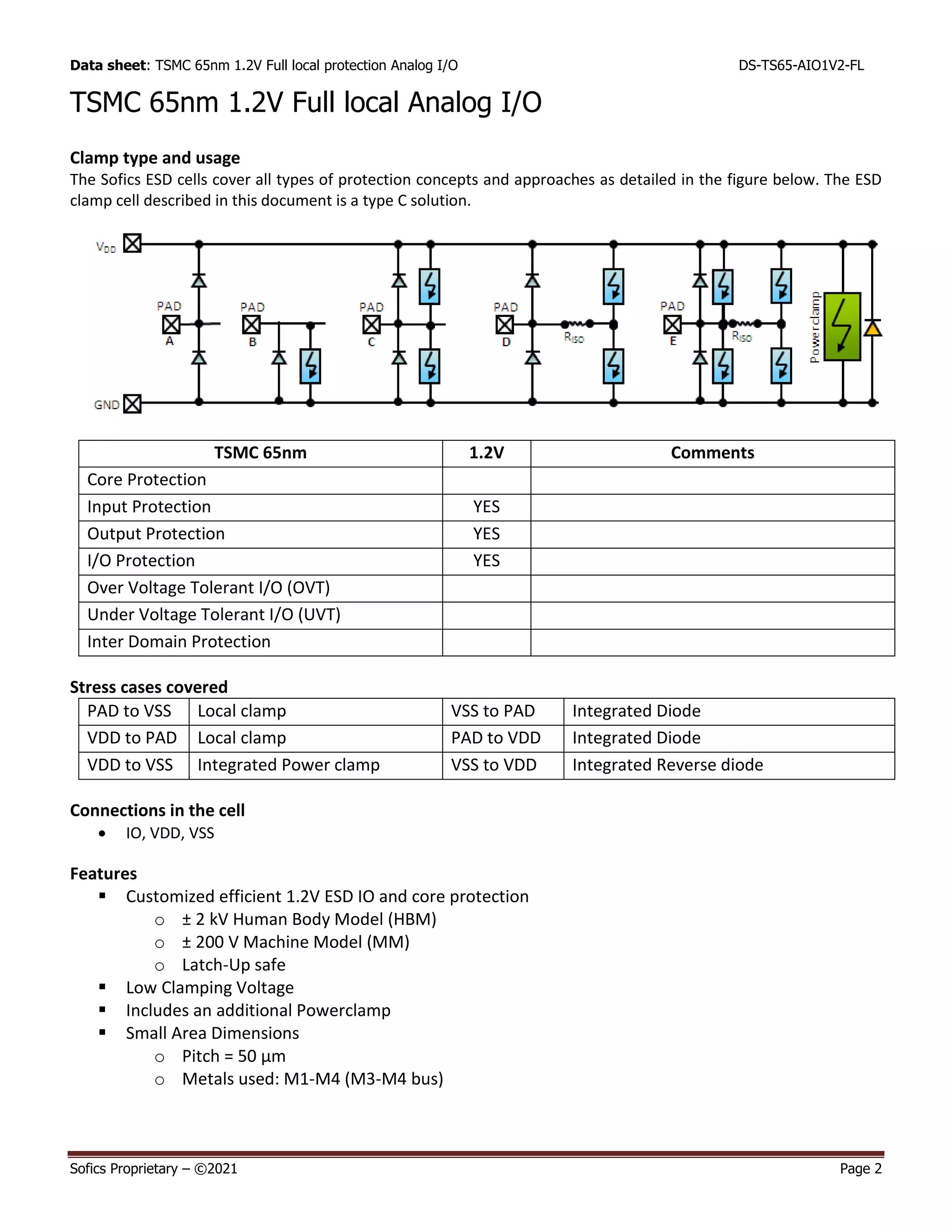
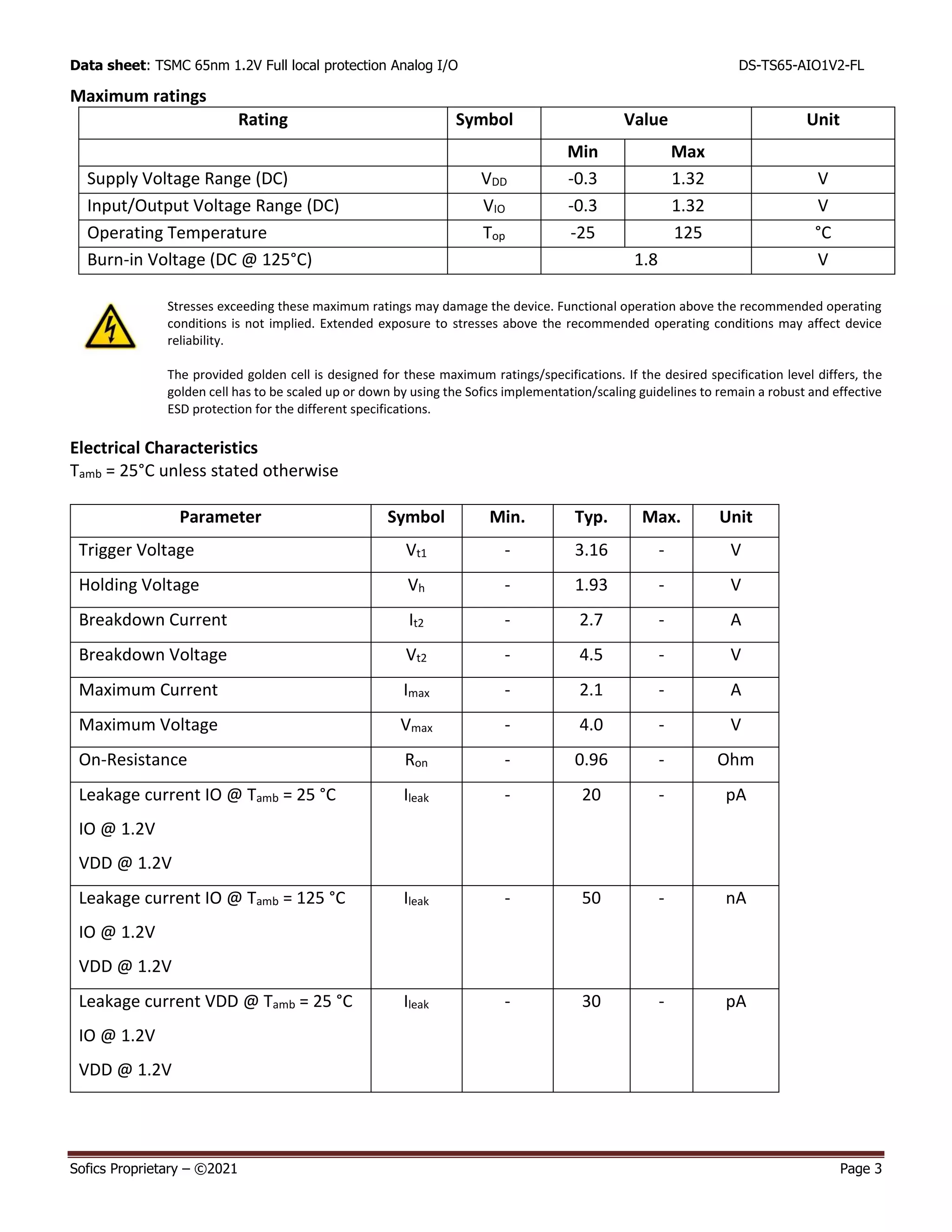
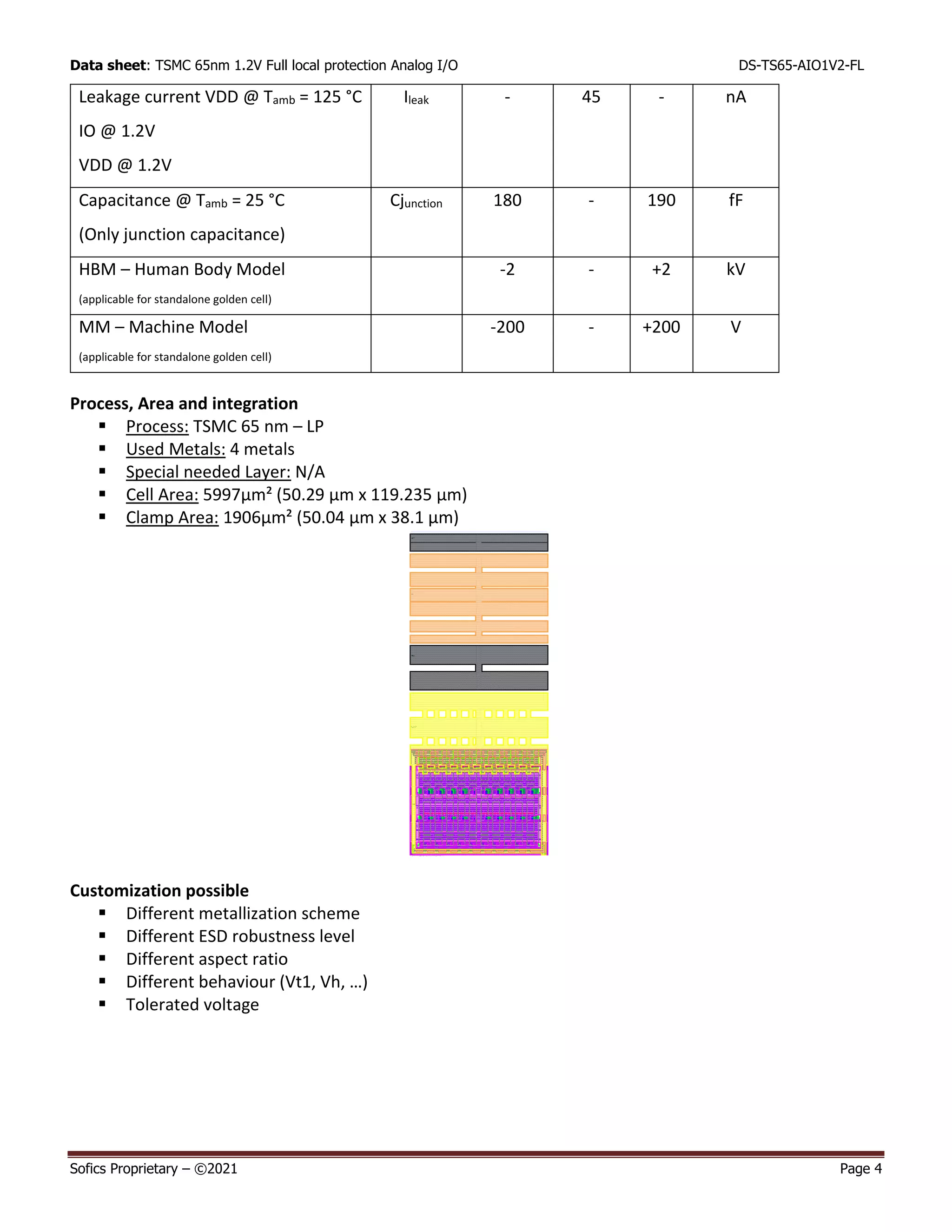
Data sheet 1.2V Full local Analog I/O
TSMC 65nm
Sofics has verified its TakeCharge ESD protection clamps on technology
nodes between 0.25um CMOS down to 5nm across various fabs and
foundries. The ESD clamps are silicon and product proven in more than 4500
mass produced IC-products. The cells provide competitive advantage
through improved yield, reduced silicon footprint and enable advanced
multimedia and wireless interfaces like HDMI, USB 3.0, SATA, WIFI, GPS and
Bluetooth.
The Analog I/O clamp described in this document can be used for 1.2V pads
in the TSMC 65nm CMOS technology.
Data sheet: TSMC 65nm 1.2V Full local protection Analog I/O DS-TS65-AIO1V2-FL
Sofics Proprietary – ©2021 Page 2
TSMC 65nm 1.2V Full local Analog I/O
Clamp type and usage
The Sofics ESD cells cover all types of protection concepts and approaches as detailed in the figure below. The ESD
clamp cell described in this document is a type C solution.
TSMC 65nm 1.2V Comments
Core Protection
Input Protection YES
Output Protection YES
I/O Protection YES
Over Voltage Tolerant I/O (OVT)
Under Voltage Tolerant I/O (UVT)
Inter Domain Protection
Stress cases covered
PAD to VSS Local clamp VSS to PAD Integrated Diode
VDD to PAD Local clamp PAD to VDD Integrated Diode
VDD to VSS Integrated Power clamp VSS to VDD Integrated Reverse diode
Connections in the cell
• IO, VDD, VSS
Features
▪ Customized efficient 1.2V ESD IO and core protection
o ± 2 kV Human Body Model (HBM)
o ± 200 V Machine Model (MM)
o Latch-Up safe
▪ Low Clamping Voltage
▪ Includes an additional Powerclamp
▪ Small Area Dimensions
o Pitch = 50 µm
o Metals used: M1-M4 (M3-M4 bus)
Data sheet: TSMC 65nm 1.2V Full local protection Analog I/O DS-TS65-AIO1V2-FL
Sofics Proprietary – ©2021 Page 3
Maximum ratings
Rating Symbol Value Unit
Min Max
Supply Voltage Range (DC) VDD -0.3 1.32 V
Input/Output Voltage Range (DC) VIO -0.3 1.32 V
Operating Temperature Top -25 125 °C
Burn-in Voltage (DC @ 125°C) 1.8 V
Stresses exceeding these maximum ratings may damage the device. Functional operation above the recommended operating
conditions is not implied. Extended exposure to stresses above the recommended operating conditions may affect device
reliability.
The provided golden cell is designed for these maximum ratings/specifications. If the desired specification level differs, the
golden cell has to be scaled up or down by using the Sofics implementation/scaling guidelines to remain a robust and effective
ESD protection for the different specifications.
Electrical Characteristics
Tamb = 25°C unless stated otherwise
Parameter Symbol Min. Typ. Max. Unit
Trigger Voltage Vt1 - 3.16 - V
Holding Voltage Vh - 1.93 - V
Breakdown Current It2 - 2.7 - A
Breakdown Voltage Vt2 - 4.5 - V
Maximum Current Imax - 2.1 - A
Maximum Voltage Vmax - 4.0 - V
On-Resistance Ron - 0.96 - Ohm
Leakage current IO @ Tamb = 25 °C
IO @ 1.2V
VDD @ 1.2V
Ileak - 20 - pA
Leakage current IO @ Tamb = 125 °C
IO @ 1.2V
VDD @ 1.2V
Ileak - 50 - nA
Leakage current VDD @ Tamb = 25 °C
IO @ 1.2V
VDD @ 1.2V
Ileak - 30 - pA
Data sheet: TSMC 65nm 1.2V Full local protection Analog I/O DS-TS65-AIO1V2-FL
Sofics Proprietary – ©2021 Page 4
Leakage current VDD @ Tamb = 125 °C
IO @ 1.2V
VDD @ 1.2V
Ileak - 45 - nA
Capacitance @ Tamb = 25 °C
(Only junction capacitance)
Cjunction 180 - 190 fF
HBM – Human Body Model
(applicable for standalone golden cell)
-2 - +2 kV
MM – Machine Model
(applicable for standalone golden cell)
-200 - +200 V
Process, Area and integration
▪ Process: TSMC 65 nm – LP
▪ Used Metals: 4 metals
▪ Special needed Layer: N/A
▪ Cell Area: 5997µm² (50.29 µm x 119.235 µm)
▪ Clamp Area: 1906µm² (50.04 µm x 38.1 µm)
Customization possible
▪ Different metallization scheme
▪ Different ESD robustness level
▪ Different aspect ratio
▪ Different behaviour (Vt1, Vh, …)
▪ Tolerated voltage
Data sheet: TSMC 65nm 1.2V Full local protection Analog I/O DS-TS65-AIO1V2-FL
Sofics Proprietary – ©2021 Page 5
About Sofics
Sofics is a foundry independent semiconductor IP provider that has supported 100+ companies worldwide
with customized/specialty Analog IOs and on-chip ESD protection. Fabless companies using Sofics IP can
enable higher performance, higher robustness and reduce design time and cost. Our technology has been
characterized on 10 foundries including advanced nodes at TSMC, UMC, GF.
Sofics IP is used for design projects at 4 of the top-5 semiconductor companies, 6 out of the top-10. The
technology has been silicon proven on more than 50 different processes and integrated into more than 4500
IC designs since 2000.
Sofics is a TSMC 9000™ quality approved ESD solutions provider for TSMC processes
Contact us
Sofics BV
BTW BE 0472.687.037 RPR Gent afdeling Oostende
Engineering office
Sint-Godelievestraat 32
9880 Aalter, Belgium
Website: www.sofics.com
Connect through email: info@mail.sofics.com
Notes
As is the case with many published ESD design solutions, the techniques and protection solutions described
in this data sheet are protected by patents and patents pending and cannot be copied freely. PowerQubic,
TakeCharge, and Sofics are trademarks of Sofics BV.

1.2V Analog I/O with full local ESD protection for TSMC 65nm technology

  • 1.
    Data sheet 1.2VFull local Analog I/O TSMC 65nm Sofics has verified its TakeCharge ESD protection clamps on technology nodes between 0.25um CMOS down to 5nm across various fabs and foundries. The ESD clamps are silicon and product proven in more than 4500 mass produced IC-products. The cells provide competitive advantage through improved yield, reduced silicon footprint and enable advanced multimedia and wireless interfaces like HDMI, USB 3.0, SATA, WIFI, GPS and Bluetooth. The Analog I/O clamp described in this document can be used for 1.2V pads in the TSMC 65nm CMOS technology.
  • 2.
    Data sheet: TSMC65nm 1.2V Full local protection Analog I/O DS-TS65-AIO1V2-FL Sofics Proprietary – ©2021 Page 2 TSMC 65nm 1.2V Full local Analog I/O Clamp type and usage The Sofics ESD cells cover all types of protection concepts and approaches as detailed in the figure below. The ESD clamp cell described in this document is a type C solution. TSMC 65nm 1.2V Comments Core Protection Input Protection YES Output Protection YES I/O Protection YES Over Voltage Tolerant I/O (OVT) Under Voltage Tolerant I/O (UVT) Inter Domain Protection Stress cases covered PAD to VSS Local clamp VSS to PAD Integrated Diode VDD to PAD Local clamp PAD to VDD Integrated Diode VDD to VSS Integrated Power clamp VSS to VDD Integrated Reverse diode Connections in the cell • IO, VDD, VSS Features ▪ Customized efficient 1.2V ESD IO and core protection o ± 2 kV Human Body Model (HBM) o ± 200 V Machine Model (MM) o Latch-Up safe ▪ Low Clamping Voltage ▪ Includes an additional Powerclamp ▪ Small Area Dimensions o Pitch = 50 µm o Metals used: M1-M4 (M3-M4 bus)
  • 3.
    Data sheet: TSMC65nm 1.2V Full local protection Analog I/O DS-TS65-AIO1V2-FL Sofics Proprietary – ©2021 Page 3 Maximum ratings Rating Symbol Value Unit Min Max Supply Voltage Range (DC) VDD -0.3 1.32 V Input/Output Voltage Range (DC) VIO -0.3 1.32 V Operating Temperature Top -25 125 °C Burn-in Voltage (DC @ 125°C) 1.8 V Stresses exceeding these maximum ratings may damage the device. Functional operation above the recommended operating conditions is not implied. Extended exposure to stresses above the recommended operating conditions may affect device reliability. The provided golden cell is designed for these maximum ratings/specifications. If the desired specification level differs, the golden cell has to be scaled up or down by using the Sofics implementation/scaling guidelines to remain a robust and effective ESD protection for the different specifications. Electrical Characteristics Tamb = 25°C unless stated otherwise Parameter Symbol Min. Typ. Max. Unit Trigger Voltage Vt1 - 3.16 - V Holding Voltage Vh - 1.93 - V Breakdown Current It2 - 2.7 - A Breakdown Voltage Vt2 - 4.5 - V Maximum Current Imax - 2.1 - A Maximum Voltage Vmax - 4.0 - V On-Resistance Ron - 0.96 - Ohm Leakage current IO @ Tamb = 25 °C IO @ 1.2V VDD @ 1.2V Ileak - 20 - pA Leakage current IO @ Tamb = 125 °C IO @ 1.2V VDD @ 1.2V Ileak - 50 - nA Leakage current VDD @ Tamb = 25 °C IO @ 1.2V VDD @ 1.2V Ileak - 30 - pA
  • 4.
    Data sheet: TSMC65nm 1.2V Full local protection Analog I/O DS-TS65-AIO1V2-FL Sofics Proprietary – ©2021 Page 4 Leakage current VDD @ Tamb = 125 °C IO @ 1.2V VDD @ 1.2V Ileak - 45 - nA Capacitance @ Tamb = 25 °C (Only junction capacitance) Cjunction 180 - 190 fF HBM – Human Body Model (applicable for standalone golden cell) -2 - +2 kV MM – Machine Model (applicable for standalone golden cell) -200 - +200 V Process, Area and integration ▪ Process: TSMC 65 nm – LP ▪ Used Metals: 4 metals ▪ Special needed Layer: N/A ▪ Cell Area: 5997µm² (50.29 µm x 119.235 µm) ▪ Clamp Area: 1906µm² (50.04 µm x 38.1 µm) Customization possible ▪ Different metallization scheme ▪ Different ESD robustness level ▪ Different aspect ratio ▪ Different behaviour (Vt1, Vh, …) ▪ Tolerated voltage
  • 5.
    Data sheet: TSMC65nm 1.2V Full local protection Analog I/O DS-TS65-AIO1V2-FL Sofics Proprietary – ©2021 Page 5 About Sofics Sofics is a foundry independent semiconductor IP provider that has supported 100+ companies worldwide with customized/specialty Analog IOs and on-chip ESD protection. Fabless companies using Sofics IP can enable higher performance, higher robustness and reduce design time and cost. Our technology has been characterized on 10 foundries including advanced nodes at TSMC, UMC, GF. Sofics IP is used for design projects at 4 of the top-5 semiconductor companies, 6 out of the top-10. The technology has been silicon proven on more than 50 different processes and integrated into more than 4500 IC designs since 2000. Sofics is a TSMC 9000™ quality approved ESD solutions provider for TSMC processes Contact us Sofics BV BTW BE 0472.687.037 RPR Gent afdeling Oostende Engineering office Sint-Godelievestraat 32 9880 Aalter, Belgium Website: www.sofics.com Connect through email: info@mail.sofics.com Notes As is the case with many published ESD design solutions, the techniques and protection solutions described in this data sheet are protected by patents and patents pending and cannot be copied freely. PowerQubic, TakeCharge, and Sofics are trademarks of Sofics BV.