Download as PPS, PPTX
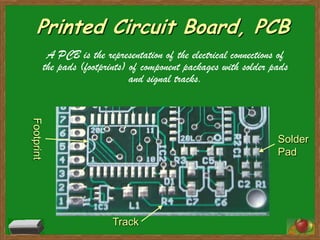


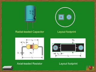


A printed circuit board (PCB) represents the electrical connections between component packages and pads using copper tracks. Common PCB materials include copper conducting layers and insulating epoxy resin layers. Footprints define the pattern components occupy on the board. Initially, components are placed loosely in airwire form, resembling a messy ratsnest that is later disentangled through routing. Routing connects components by selecting shortest paths between pads while adhering to design guidelines regarding component placement, trace widths, and thermal reliefs.