
![11/3/2020 Arpan Deyasi, RCCIIT, India 7
Band Diagram of MOS [Al-SiO2-Si(n)]
EFm
χ =
4.25
eV
ECI
χ = 0.9 eV
EVI
Eg =
8.76
eV
ECS
EVS
Eg =
1.12
eV
χ =
4.05
eV
EFS
ΦF
E0
(Al) (SiO2) (Si)](https://image.slidesharecdn.com/mod6presentation1-201103132543/85/Foundation-of-MOS-Capacitor-7-320.jpg)
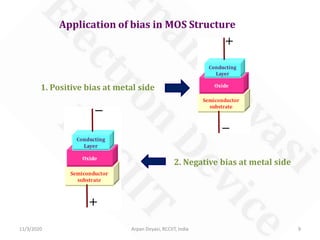
![11/3/2020 Arpan Deyasi, RCCIIT, India 10
Property of semiconductor will play a vital role
[i] Al-SiO2-Si(n)
[ii] Al-SiO2-Si(p)
1. Positive bias at metal side
1. Positive bias at metal side
2. Negative bias at metal side
2. Negative bias at metal side](https://image.slidesharecdn.com/mod6presentation1-201103132543/85/Foundation-of-MOS-Capacitor-10-320.jpg)
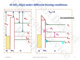
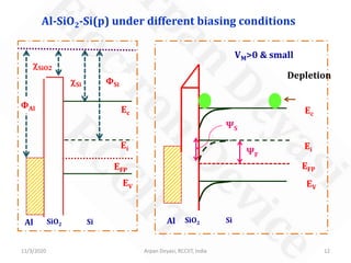
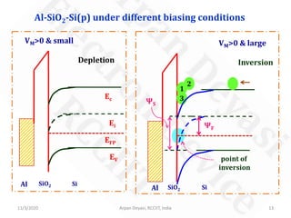
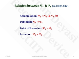
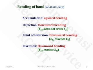

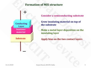
This document discusses the MOS capacitor structure. It begins by defining the key components of a MOS capacitor as a semiconductor substrate, insulating oxide layer, and conducting metal layer. The document then examines the band diagram of an n-type silicon MOS capacitor at zero bias. It explains how applying a positive or negative bias to the metal layer can cause the band diagram to deviate, resulting in accumulation, depletion, or inversion at the silicon surface. Key relationships between the metal and silicon surface potentials are also defined for a p-type silicon MOS capacitor under varying bias conditions.