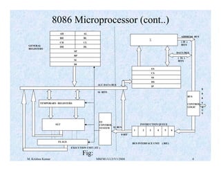
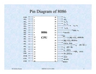
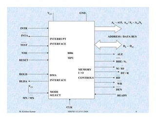
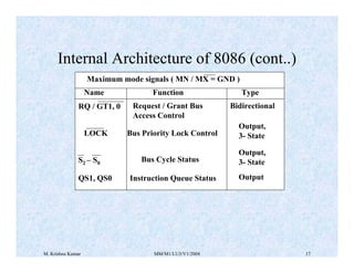
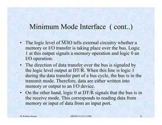
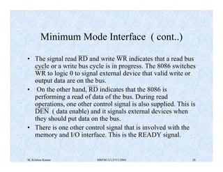
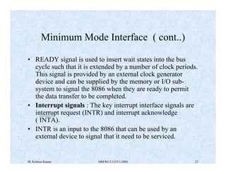
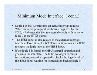
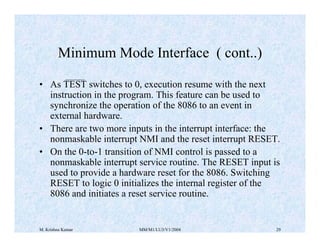
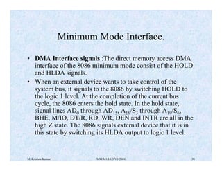
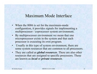
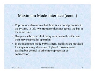
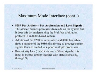
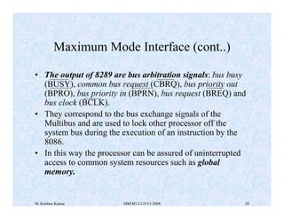
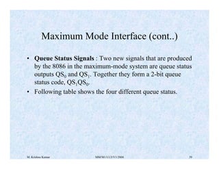
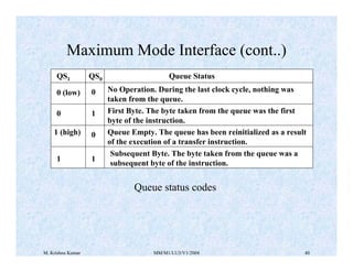
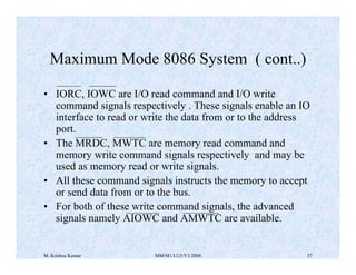
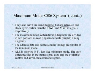
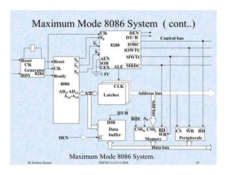
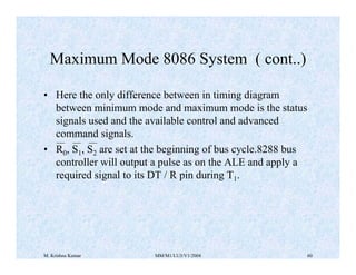
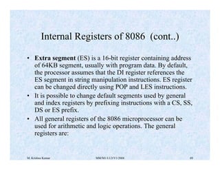
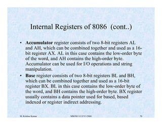
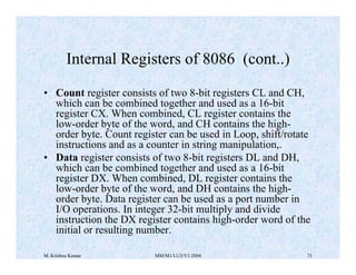
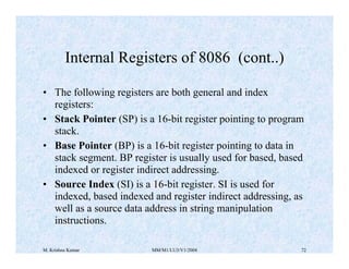
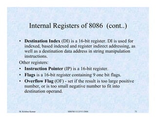
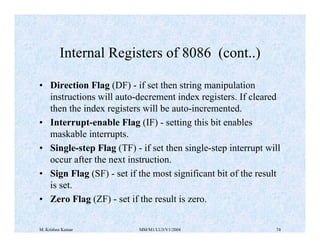
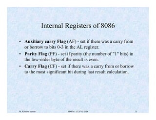
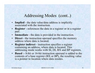
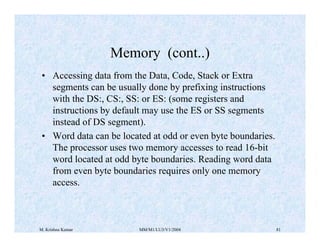
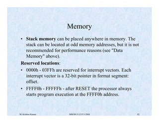
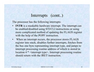
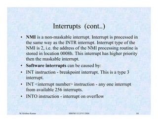
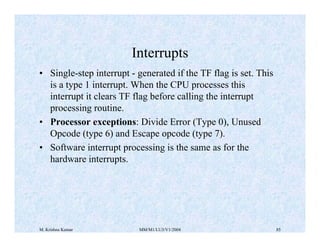
The document provides details about the 8086 microprocessor architecture. Some key points:
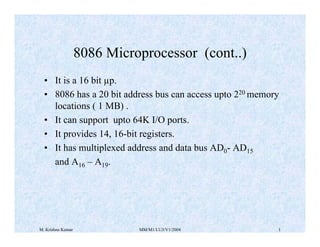
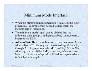
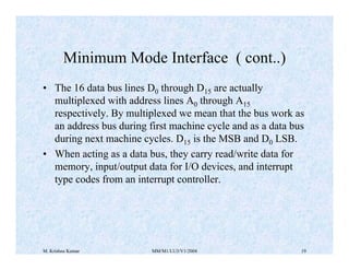
- The 8086 is a 16-bit microprocessor that can access up to 1MB of memory using a 20-bit address bus and supports up to 64K I/O ports.
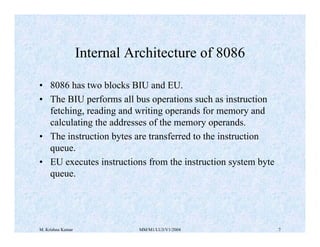
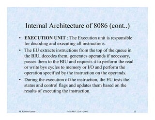
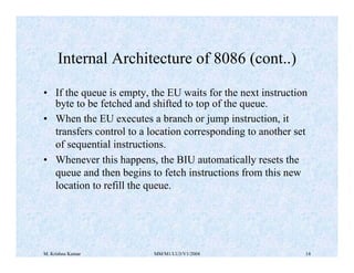
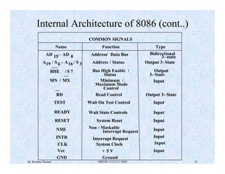
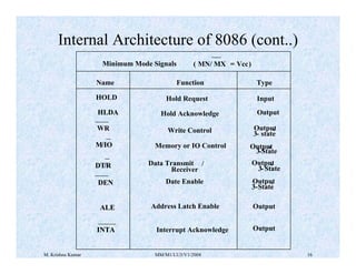
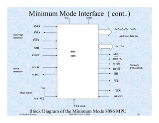
- It has an internal architecture divided into a Bus Interface Unit (BIU) and Execution Unit (EU) that allows for overlapping of instruction fetching and execution via pipelining.
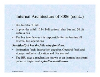
- The BIU handles external bus operations like instruction fetching and memory/I/O access. The EU decodes and executes instructions, performing operations on operands retrieved by the BIU.