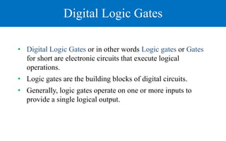
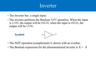
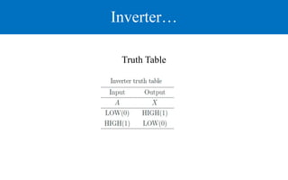
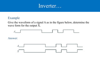
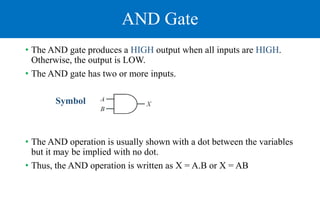
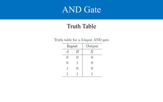
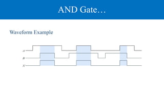
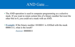
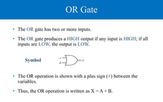
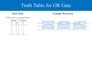
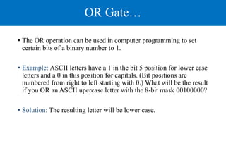
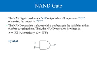
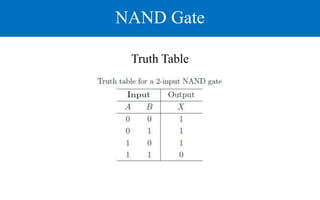
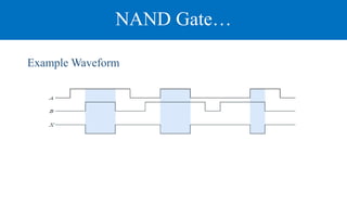
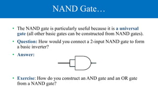
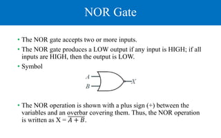
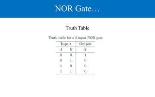
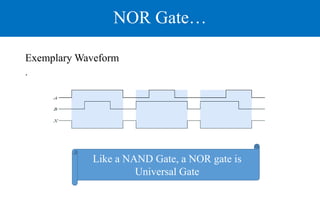
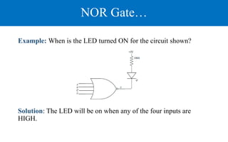
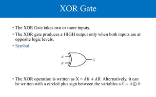
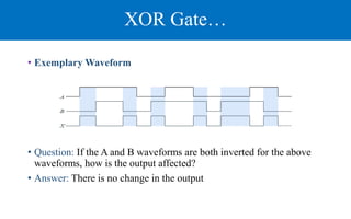
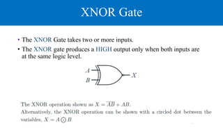
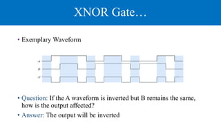
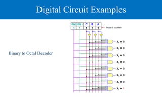
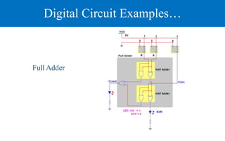
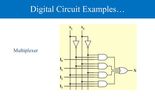
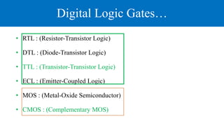
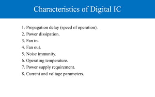
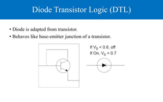
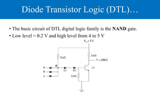
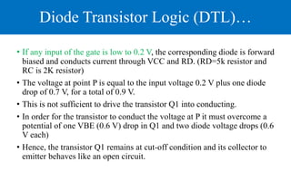
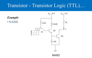
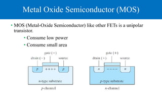
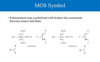
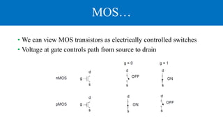
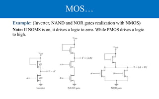
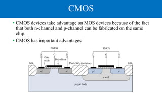
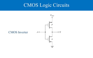
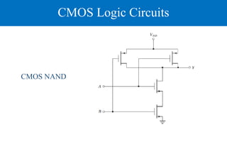
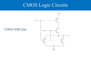
Coefficient of Thermal Expansion and their Importance.pptx
Chapter 3.pptx
1. Chapter Three
Digital Logic Gates (Lec 1)
Prepared by: Esubalew Mulat
Target Group: 2nd Year CS Students
Adapted from Addisalem Hailegnaw, DBU
.
Debre Berhan University, March 2015 E.C.
2. Topics
• Introduction to Logic Gates
• Types of Logic Gates
• Introduction to Digital Logic Family
• Realization of Logic Gates
3. Digital Logic Gates
• Digital Logic Gates or in other words Logic gates or Gates
for short are electronic circuits that execute logical
operations.
• Logic gates are the building blocks of digital circuits.
• Generally, logic gates operate on one or more inputs to
provide a single logical output.
4. Digital Logic Gates…
• Electronic gates require a power supply.
• Gate INPUTS are driven by voltages having two nominal
values.
• The OUTPUT of a gate provides only two nominal values of
voltage.
• There is always a time delay between an input being applied and
the output responding.
6. Inverter
• The Inverter has a single input.
• The inverter performs the Boolean NOT operation. When the input
is LOW, the output will be HIGH; when the input is HIGH, the
output will be LOW.
Symbol
• The NOT operation (complement) is shown with an overbar.
• The Boolean expression for the aforementioned inverter is X = 𝐴
9. AND Gate
• The AND gate produces a HIGH output when all inputs are HIGH.
Otherwise, the output is LOW.
• The AND gate has two or more inputs.
Symbol
• The AND operation is usually shown with a dot between the variables
but it may be implied with no dot.
• Thus, the AND operation is written as X = A.B or X = AB
12. AND Gate…
• The AND operation is used in computer programming as a selective
mask. If you want to retain certain bits of a binary number but reset the
other bits to 0, you could set a mask with an AND.
• Example: If the binary number 10100011 is ANDed with the mask
00001111, what is the result?
Answer: 00000011
13. OR Gate
• The OR gate has two or more inputs.
• The OR gate produces a HIGH output if any input is HIGH; if all
inputs are LOW, the output is LOW.
Symbol
• The OR operation is shown with a plus sign (+) between the
variables.
• Thus, the OR operation is written as X = A + B.
15. OR Gate…
• The OR operation can be used in computer programming to set
certain bits of a binary number to 1.
• Example: ASCII letters have a 1 in the bit 5 position for lower case
letters and a 0 in this position for capitals. (Bit positions are
numbered from right to left starting with 0.) What will be the result
if you OR an ASCII upercase letter with the 8-bit mask 00100000?
• Solution: The resulting letter will be lower case.
16. NAND Gate
• The NAND gate produces a LOW output when all inputs are HIGH;
otherwise, the output is HIGH.
• The NAND operation is shown with a dot between the variables and an
overbar covering them. Thus, the NAND operation is written as
X = 𝐴𝐵 (Alternatively, X = 𝐴. 𝐵)
Symbol
19. NAND Gate…
• The NAND gate is particularly useful because it is a universal
gate (all other basic gates can be constructed from NAND gates).
• Question: How would you connect a 2-input NAND gate to form
a basic inverter?
• Answer:
• Exercise: How do you construct an AND gate and an OR gate
from a NAND gate?
20. NOR Gate
• The NOR gate accepts two or more inputs.
• The NOR gate produces a LOW output if any input is HIGH; if all
inputs are HIGH, then the output is LOW.
• Symbol
• The NOR operation is shown with a plus sign (+) between the
variables and an overbar covering them. Thus, the NOR operation
is written as X = 𝐴 + 𝐵.
23. NOR Gate…
Example: When is the LED turned ON for the circuit shown?
Solution: The LED will be on when any of the four inputs are
HIGH.
24. XOR Gate
• The XOR Gate takes two or more inputs.
• The XOR gate produces a HIGH output only when both inputs are at
opposite logic levels.
• Symbol
• The XOR operation is written as X = 𝐴𝐵 + 𝐴𝐵. Alternatively, it can
be written with a circled plus sign between the variables as
25. XOR Gate…
• Exemplary Waveform
• Question: If the A and B waveforms are both inverted for the above
waveforms, how is the output affected?
• Answer: There is no change in the output
26. XNOR Gate
• The XNOR Gate takes two or more inputs.
• The XNOR gate produces a HIGH output only when both inputs are
at the same logic level.
27. XNOR Gate…
• Exemplary Waveform
• Question: If the A waveform is inverted but B remains the same,
how is the output affected?
• Answer: The output will be inverted
36. Digital Logic Gates
• Digital ICs can be classified by the specific circuit
technology to which they belong.
• The circuit technology is referred to as a digital logic family.
• Each logic family has its own basic electronic circuit upon
which more complex digital circuits and components are
developed.
• The basic circuit in each technology is a NAND, NOR, or
Inverter gate.
38. Characteristics of Digital IC
1. Propagation delay (speed of operation).
2. Power dissipation.
3. Fan in.
4. Fan out.
5. Noise immunity.
6. Operating temperature.
7. Power supply requirement.
8. Current and voltage parameters.
39. Bipolar Transistor Characteristics
• Can be ‘npn’ or ‘pnp’
• Germanium or Silicon
• Bipolar IC transistors are made with silicon and are usually ‘npn’
type.
42. Resistor Transistor Logic (RTL)
• The basic circuit of RTL digital logic family is the NOR gate.
• Low level = 0.2 V and high level from 1 to 3.6V
43. Resistor Transistor Logic (RTL)
• The RTL logic circuit has many drawbacks.
• The resistors increase the input resistance and reduce the switching
speed of the circuit.
• This degrades the rise and fall times of any input pulse.
(Read More on It!)
44. Diode Transistor Logic (DTL)
• Diode is adapted from transistor.
• Behaves like base-emitter junction of a transistor.
45. Diode Transistor Logic (DTL)…
• The basic circuit of DTL digital logic family is the NAND gate.
• Low level = 0.2 V and high level from 4 to 5 V
46. Diode Transistor Logic (DTL)…
• If any input of the gate is low to 0.2 V, the corresponding diode is forward
biased and conducts current through VCC and RD. (RD=5k resistor and
RC is 2K resistor)
• The voltage at point P is equal to the input voltage 0.2 V plus one diode
drop of 0.7 V, for a total of 0.9 V.
• This is not sufficient to drive the transistor Q1 into conducting.
• In order for the transistor to conduct the voltage at P it must overcome a
potential of one VBE (0.6 V) drop in Q1 and two diode voltage drops (0.6
V each)
• Hence, the transistor Q1 remains at cut-off condition and its collector to
emitter behaves like an open circuit.
47. Diode Transistor Logic (DTL)…
• If all the inputs of the gate are high to 5 V, all the diodes are reverse
biased and the current will flow through RD, D1, D2, and the base of the
transistor.
• The transistor is now driven to saturation region. The voltage at P is
equal to one VBE drop plus two diode drops across D1 and D2, or 3 ×
0.7V = 2.1 V (VBE drop is 0.7 V while conducting and forward biased
diode drop becomes 0.7 V).
• This conforms that all the input diodes are reverse biased and off. With
the transistor at saturated condition, the output drops to VCE(sat) = 0.2 V,
which is low level for the gate.
48. Transistor - Transistor Logic (TTL)
• Replaces diode with a transistor
• Open collector TTL
• L = 0.2 V and H = 2.4 to 5 V
• The multiple emitters in Q1 behave like the input diodes in DTL,
because they form a p-n junction.
49. Transistor - Transistor Logic (TTL)…
Debre Berhan University, February 2013 E.C.
Example
• NAND
50. Emitter Coupled Logic (ECL)
• Non-saturated digital logic family.
• Propagation Delay : 1~ 2 ns (The fastest)
• Was mostly used in systems requiring very high speed.
E.g. Mainframe computers.
• Very bad power dissipation and noise immunity !!!
• Noise margin : 0.3 V
• High fan-out possible
• Obsolete !!
51. Metal Oxide Semiconductor (MOS)
• MOS (Metal-Oxide Semiconductor) like other FETs is a unipolar
transistor.
• Consume low power
• Consume small area
53. MOS…
• We can view MOS transistors as electrically controlled switches
• Voltage at gate controls path from source to drain
54. MOS…
Example: (Inverter, NAND and NOR gates realization with NMOS)
Note: If NOMS is on, it drives a logic to zero. While PMOS drives a logic
to high.
55. CMOS
• CMOS devices take advantage on MOS devices because of the fact
that both n-channel and p-channel can be fabricated on the same
chip.
• CMOS has important advantages
56. CMOS
• CMOS devices take advantage on MOS devices because of the fact
that both n-channel and p-channel can be fabricated on the same
chip.
• CMOS has important advantages
extremely low power use (a reason of its popularity)
higher noise immunity
high fan out capability and
wide range of supply voltage
Simpler interface with other logic circuits